Domain Switching Kinetics in Disordered Ferroelectric Thin Films
Abstract
We investigated domain kinetics by measuring the polarization switching behaviors of polycrystalline Pb(Zr,Ti)O3 films, which are widely used in ferroelectric memory devices. Their switching behaviors at various electric fields and temperatures could be explained by assuming the Lorentzian distribution of domain switching times. We viewed the switching process under an electric field as a motion of the ferroelectric domain through a random medium, and we showed that the local field variation due to dipole defects at domain pinning sites could explain the intriguing distribution.
pacs:
77.80.Fm, 77.80.Dj, 77.84.DyDomain switching kinetics in ferroelectrics (FEs) under an external electric field have been extensively investigated for several decades Scott1 ; YWSo ; Lohse ; Tagantsev ; Stolichnov ; Gruverman ; Shur ; Stolichnov2 ; BHPark . The traditional approach to explain the FE switching kinetics, often called the Kolmogorov-Avrami-Ishibashi (KAI) model, is based on the classical statistical theory of nucleation and unrestricted domain growth Kolmogorov ; Avrami . For a uniformly polarized FE sample under , the KAI model gives the time ()-dependent change in polarization () as
| (1) |
where and are the effective dimension and characteristic switching time for the domain growth, respectively, and is spontaneous polarization. When the nuclei are appearing in time with the same probability, = 3 for bulk samples and = 2 for thin films remark1 . In addition, is proportional to the average distance between the nuclei, divided by the domain wall speed. Several studies have used the KAI model successfully to explain the () behaviors of FE single crystals and epitaxial thin films YWSo .
Recently, FE thin films have been intensively investigated for FE
random access memory (FeRAM) Scott1 . Most commercial FeRAM
use polycrystalline Pb(Zr,Ti)O3 (poly-PZT) films, and their
() behaviors determine the reading and writing speeds
of the FeRAM. In such non-epitaxial FE films, a domain cannot
propagate indefinitely due to pinning caused by numerous defects,
so the KAI model cannot be applied. Therefore, it is important
both scientifically and technologically to clarify the domain
switching kinetics of
polycrystalline FE films.
Numerous studies have examined the behaviors
of polycrystalline FE films, and the reported results vary
markedly Shur ; Lohse ; Tagantsev ; Stolichnov ; Gruverman . Lohse
measured the polarization switching currents of
poly-PZT films, and showed that () slowed
significantly compared to Eq. (1) Lohse . Tagantsev
observed similar phenomena for poly-PZT films. To explain
these behaviors, they developed the nucleation-limited-switching
(NLS) model. They assumed that films consist of several areas that
have independent switching kinetics:
| (2) |
where (log ) is the distribution function for log Tagantsev . They assumed a very broad mesa-like function for (log ), and could explain their () data. The same authors also studied La-doped poly-PZT films and found that at room temperature is limited mainly by nucleation, while at a low temperature (), the switching kinetics are governed by domain wall motion, implying the validity of the KAI model Stolichnov .
In this Letter, we investigate the polarization switching
behaviors of poly-PZT films. We can explain the measured ()
in terms of the Lorentzian distribution function for
(log ), irrespective of . We show that such
distribution arises from local field variation in a disordered
system with dipole-dipole
interactions.
Note that (111)-oriented poly-PZT films with a Ti
concentration near 0.7 are the most widely used material in FeRAM
applications. We prepared our polycrystalline
PbZr0.3Ti0.7O3 thin film on Pt/Ti/SiO2/Si
substrates using the sol-gel method. The poly-PZT film had a
thickness of 150 nm. X-ray diffraction studies showed that it has
the (111)-preferred orientation, and scanning electron microscopy
studies indicated that our poly-PZT film consists of grains with a
size of about 200 nm. We deposited Pt top electrodes using
sputtering with a shadow mask. The areas of the top electrodes
were about 7.910-9 m2.
We obtain the () values of our Pt/PZT/Pt capacitors
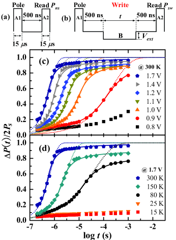
using pulse measurements Tagantsev ; YWSo ; YSKim ; JYJo1 . Figure
1(a) shows the pulse trains used to measure the non-switching
polarization change (). Using pulse A1, we poled all the
FE domains in one direction. Then, we applied pulse A2 with the
same polarity, and measure the current passing a sensing resistor.
By integrating the current, we could obtain the values.
Figure 1(b) shows the pulse trains used to measure the switching
polarization (). Inserting pulse B with the opposite
polarity between pulses A1 and A2, we could reverse some portion
of the FE domains, so the difference between the values of
and represents the polarization change due to
domain switching, namely (). We varied from 200
ns to 1 ms, and from 0.8 to 4 V. The value of
can be estimated easily by dividing by the film
thickness. At of 80300 K, we used pulses A1 and A2 with
a height of 4 V, which was larger than the coercive voltage. Below
80 K, the coercive voltage increases, so we increased
the pulse height to 6 V remark2 .
Figure 1(c) shows the values of ()/2
at room temperature with numerous values of . Figure 1(d)
shows the values of ()/2 at various with
= 1.7 V. The dotted lines in both figures are the curves
best fitting Eq. (1). The KAI model predictions deviated markedly
from the experimental () values in the late
switching stage, in agreement with Gruverman .
Gruverman . In addition, the best fitting results with the
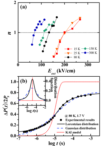
KAI model gave unreasonable values of . As shown in Fig. 2(a),
the values of varied markedly with and . In
addition, in the low region, we obtained values much
smaller than 1, which are not proper as an effective dimension of
domain growth. Therefore, Eq. (1) fails to describe the
polarization switching behaviors of our PZT films.
To explain the measured (), we tried simple functions for (log ) in Eq. (2). The opposite domain, once nucleated, will propagate inside the film, so we fixed =2. The solid circles in Fig. 2(b) show the experimental t at 80 K with = 1.7 V. For (log ), we tried the delta, Gaussian, and Lorentzian distribution functions, as shown in the inset. The dotted line indicates the fitting results using Eq. (2) with a delta function. Note that this curve corresponds to a fit with the KAI model, and thus the classical theory cannot explain our experimental data. The dashed line shows the Gaussian fitting results. Although this fitting seems reasonable, some discrepancies occur. The solid black shows the fitting results with the Lorentzian distribution:
| (3) |
where is a normalization constant, and (log ) is the half-width at half-maximum (a central value) remark3 . The Lorentzian fit can account for our observed () behaviors quite well.
We applied the Lorentzian fit to all of the other experimental
() data. As shown by the solid lines in Figs. 1(c)
and (d), the Lorentzian fit provides excellent explanations.
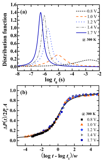
Figure 3(a) presents the Lorentzian distribution functions used
for the 300 K data. As increases, log and
decrease. We rescaled the experimental ()/2
data using (log - log )/. All the data merge into a
single line, an arctangent function remark3 , as shown in
Fig. 3(b). Although not indicated in this figure, the experimental
data for all other also merged with this line. This scaling
behavior suggests that the Lorentzian distribution function for
log is intrinsic.
Note that (log ) follows not the Gaussian
distribution, but the Lorentzian distribution. For a statistically
independent random process, it is a basic statistical rule that
the resulting distribution should become Gaussian, regardless of
the process details Reif . For example, impurities (or
crystal defects) inside a real crystal result in inhomogeneous
broadening of the light absorption line, which has a
Gaussian line shape.
However, some studies have observed that magnetic
resonance line broadening of randomly distributed dipole
impurities follows the Lorentzian distribution Vleck . The
first rigorous theoretical
result for this problem is that of Anderson, who showed
that the distribution of any interaction field component in the
system of dilute aligned dipoles should be Lorentzian
Anderson ; Klauder . Polycrystalline FE films should contain
many dipole defects that will act as pinning sites for the domain
wall motion. To explain our observed Lorentzian distribution of
log , we assume that a local field exists at
the FE domain pinning sites and that it has a Lorentzian
distribution:
| (4) |
where is the half-width at half-maximum of the
distribution function, related to the concentration
of
pinning sites.
In the low region, the domain wall motion should
be governed by thermal activation process at the pinning sites.
Without effects, thermal activation results in a
domain wall speed in the form 1/
[-(/)(/)], where is the energy
barrier and is the threshold electric field for pinned
domains Triscone . Since results in a change
in the effective electric field at pinning sites, the associated
can be expressed as
| (5) |
Then, the distribution of results in a distribution in log , using the relation . With
| (6) |
and
| (7) |
we can obtain the desired Lorentzian distribution for (log ), i.e., Eq. (3), from Eqs. (4) and (5).
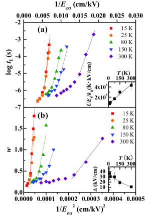
Our experimental values for log and agree with the
analytical forms. Figures 4(a) and (b) plot log
1/ and 1/ at various ,
respectively. Both log and follow the expected
-dependence in the low region. Note that Eq.
(6) is consistent with Merz’s law Merz , which states that
the current coming from FE polarization switching should have a
characteristic time of (/), where
is the activation field. Using this empirical law, several studies
have measured values. For example, So . reported
1700 kV/cm for 100-nm-thick epitaxial PZT films
YWSo , and Scott . reported 270
kV/cm for 350-nm-thick poly-PZT films Scott2 . These values
are consistent with our room temperature value of
/, i.e., 1400
kV/cm.
Our model viewed the FE domain switching kinetics as
domain wall motion driven by with a random pinning
potential. In the low region, thermal activation at the
pinning sites can be important, resulting in the so-called domain
wall creep motion. Applying atomic force microscopy, Tybell
. Triscone and Paruch . Paruch
demonstrated that the domain-switching kinetics in epitaxial PZT
films are governed by the domain wall creep motion. Some
theoreticians studied the domain wall creep motion of an elastic
string in a random potential. They found a linear increase in
with an increase in Kolton . The insets in Fig. 4(a)
show that the value of / obtained from the linear
fits in Fig. 4(a) increase linearly with , consistent with the
theoretical prediction for Kolton . The inset in Fig.
4(b) shows obtained from the fits to Fig. 4(b). Similar
exponential decay behavior was predicted in a magnetic
resonance study of randomly distributed dipoles Klein .
At this point, we wish to compare our model with the NLS
model. Although both models use Eq. (2), the origins and forms for
(log ) are quite different. In the NLS model, the FE
film consists of numerous areas, each with its own and independent
. Subsequently, it was suggested that the individually
switched regions correspond to single grains or clusters of grains
in which the grain boundaries act as frontiers limiting the
propagation of the switched region Stolichnov2 .
Consequently, the NLS model can be applied for polycrystalline
films only, and the form of (log ) should depend on
their microstructure. Conversely, in our model, the interaction
between dipole defects inside the FE film induces a distribution
in the local field, which results in (log ). Therefore,
both point defects and the grain boundaries could act as pinning
sites. Using the Lorentzian distribution for (log ), our
model can be used for both epitaxial and polycrystalline FE films
YWSo . Using Eqs. (2) and (3) with small values, we
could successfully explain the for FE single
crystals or epitaxial thin films YWSo . We also found that
our model can explain the data for poly-PZT films
with Ti
concentrations of 0.48 and 0.65.
Note that our model for thermally activated domain
switching kinetics can be viewed as the famous problem that treats
the propagation of elastic objects driven by an external force in
presence of a pinning potential Triscone ; Paruch ; Kolton . It
can be applied to many FE films, since the domain wall motion with
a disordered pinning potential should be the dominant mechanism
for . Therefore, the studies can be
used to investigate numerous intriguing issues concerning
nonlinear systems, such as creep motion, avalanche phenomenon,
pinning/depinning transition, and so on.
In summary, we investigated the polarization switching
behaviors of (111)-oriented poly-PZT films and found that the
characteristic switching time obeyed the Lorentzian distribution.
We explained this intriguing phenomenon by introducing the local
electric field due to the defect dipole.
The authors thank D. Kim for fruitful discussions. This
study was financially supported by Creative Research Initiatives
(Functionally Integrated Oxide Heterostructure) of MOST/KOSEF.
References
- (1) Ferroelectric Memories, edited by J. F. Scott (Springer-Verlag, Berlin, 2000).
- (2) Y. W. So et al., Appl. Phys. Lett. 86, 92905 (2005) and references therein.
- (3) O. Lohse et al., J. Appl. Phys. 89, 2332 (2001).
- (4) A. K. Tagantsev et al., Phys. Rev. B 66, 214109 (2002).
- (5) I. Stolichnov et al., Appl. Phys. Lett. 83, 3362 (2003).
- (6) A. Gruverman et al., Appl. Phys. Lett. 87, 082902 (2005).
- (7) V. Shur et al., J. Appl. Phys. 84, 445 (1998).
- (8) I. Stolichnov et al., Appl. Phys. Lett. 86, 012902 (2005).
- (9) B. H. Park et al., Nature 401, 682 (1999).
- (10) N. Kolmogorov, Izv. Akad. Nauk. Ser. Math. 3, 355 (1937).
- (11) M. Avrami, J. Chem. Phys. 8, 212 (1940).
- (12) If all nuclei of opposite polarization arise through whole process, could be larger than the actual dimension.
- (13) Y. S. Kim et al., Appl. Phys. Lett. 86, 102907 (2005).
- (14) J. Y. Jo et al., Phys. Rev. Lett. 97, 247602 (2006).
- (15) Complications can occur due to charge trapping or domain pinning, called the imprint effect. Refer to Ref. Scott1 . To prevent the imprint effect, we applied a pulse with the opposite polarity at the end of each pulse train measurement (i.e., after pulse A2).
- (16) A double exponential function [-{10/10}n] with 1 can be approximated as a step function centered at log=log. As a result, Eq. (2) can be approximated as .
- (17) F. Reif, Fundamentals of Statistics and Thermal Physics (McGraw-Hill, Singapore, 1985).
- (18) J. H. V. Vleck, Phys. Rev. 74, 1168 (1948).
- (19) P. W. Anderson, Phys. Rev. 82, 342 (1951).
- (20) J. R. Klauder and P. W. Anderson, Phys. Rev. 125, 912 (1962).
- (21) T. Tybell et al., Phys. Rev. Lett. 89, 097601 (2002).
- (22) W. J. Merz, Phys. Rev. 95, 690 (1954).
- (23) J. F. Scott et al., J. Appl. Phys. 64, 787 (1998).
- (24) P. Paruch et al., Phys. Rev. Lett. 94, 197601 (2005).
- (25) A. B. Kolton et al., Phys. Rev. Lett. 94, 047002 (2005).
- (26) M. W. Klein, Phys. Rev. 173, 552 (1968).