Unconventional approaches to combine optical transparency with electrical conductivity
Abstract
Combination of electrical conductivity and optical transparency in the same material – known to be a prerogative of only a few oxides of post-transition metals, such as In, Sn, Zn and Cd – manifests itself in a distinctive band structure of the transparent conductor host. While the oxides of other elements with electronic configuration, for example, Mg, Ca, Sc and Al, also exhibit the desired optical and electronic features, they have not been considered as candidates for achieving good electrical conductivity because of the challenges of efficient carrier generation in these wide-bandgap materials. Here we demonstrate that alternative approaches to the problem not only allow attaining the transport and optical properties which compete with those in currently utilized transparent conducting oxides (TCO), but also significantly broaden the range of materials with a potential of being developed into novel functional transparent conductors.
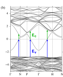
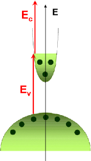
The key attribute of any conventional n-type TCO host is a highly dispersed single free-electron-like conduction band Freeman ; Mryasov ; Asahi ; Woodward ; EPL ; JACS ; JACS1 ; my-PRL . Upon proper doping, it provides both (i) high mobility of extra carriers (electrons) due to their small effective mass, and (ii) low optical absorption in the visible part of the spectrum due to high-energy inter-band transitions, e.g., Fig. 1. For the complete transparency in the visible range, the transitions from the valence band, Ev, and from the partially filled conduction band, Ec, should be larger than 3.1 eV, while the intra-band transitions as well as the plasma frequency should be smaller than 1.8 eV. The high energy dispersion also ensures a pronounced Fermi energy displacement, so-called Burstein-Moss (BM) shift, so that the optical transparency can be achieved in a material with a relatively small bandgap, for example, in CdO where the optical (direct) band gap is 2.3 eV.
Figures 1(a) and 1(b) illustrate the typical conduction band of a conventional n-type transparent conductor and how doping alters the electronic band structure of the TCO host affecting the optical transitions. It is seen that upon introduction of extra carriers into the host, a large BM shift which facilitates higher-energy transitions from the valence band (Ev), leads to a reduced energy of the transitions from the Fermi level up into the conduction band (Ec), i.e., Ev and Ec are interconnected second-hybr-gap . In other words, large carrier concentrations desired for a good conductivity, may result in an increase of the optical absorption because the Ec transitions become smaller in energy. In addition, the transitions within the partially filled band as well as plasma frequency may lead to the absorption in the long-wavelength range.
The mutual exclusiveness of the optical transmittance and electrical conductivity (see Refs. EPL ; Bellingham ; MRS-Coutts ) makes it challenging to achieve the optimal performance in a transparent conductor. Below we outline novel, unconventional ways to balance the optical and transport properties and to improve one without making a sacrifice of the other.


.1 Magnetically mediated transparent conductors
One of the possible routes to avoid compromising the optical transparency is to enhance conductivity via mobility of the carriers rather than their concentration MRS-Coutts . Recently, the mobility with more than twice the value of the commercial Sn-doped indium oxide (ITO) was observed in Mo-doped In2O3 (IMO), and it was shown that the conductivity can be significantly increased with no changes in the spectral transmittance upon doping with Mo Meng ; Yoshida ; Yoshida-effmass ; Sun . Surprisingly, introduction of the transition metal Mo which donates two more carriers per substitution compared to Sn, does not lead to the expected increase of the optical absorption or a decrease of the mobility due to the scattering on the localized Mo -states.
| Complex | M | Eg(0) | k | k | k | |
|---|---|---|---|---|---|---|
| Mo | 1.85 | 1.38 | 0.152 | 0.148 | 0.157 | 1.63 |
| Mo | 1.32 | 1.18 | 0.194 | 0.187 | 0.201 | 2.05 |
| [MoO]∙ | 0.50 | 1.26 | 0.125 | 0.123 | 0.132 | 1.27 |
| Sn | — | 0.98 | 0.201 | 0.203 | 0.205 | 2.29 |
| In2O3+e | — | 1.16 | 0.206 | 0.204 | 0.213 | 2.38 |
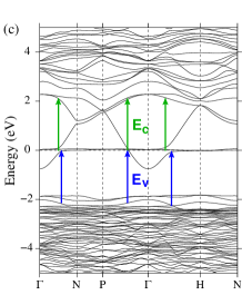
Our electronic band structure investigations of IMO revealed my-PRL that the magnetic interactions which have never been considered to play a role in combining optical transparency with electrical conductivity, ensure both high carrier mobility and low optical absorption in the visible range. As one can see from Figs. 1(c) and 1(d), strong exchange interactions split the Mo -states located in the vicinity of the Fermi level. These -states are resonant states, while the conductivity is due to the delocalized In -states which form the highly dispersed free-electron-like conduction band. In other words, the free carriers in the system flow in a background of the Mo defects which serve as strong scattering centers. Because of the exchange splitting of the Mo -states, the carriers of one spin is affected by only a half of the scattering centers, i.e., only by the Mo -states of the same spin. Therefore, the concentration of the Mo scattering centers is effectively lowered by half compared to the Mo doping level.
Figs. 1(b) and 1(c,d) show that the BM shift is less pronounced in the IMO case – despite the fact that Mo6+ donates two extra carriers as compared to Sn4+ at the same doping level. Such a low sensitivity to doping appears from the resonant Mo -states located at the Fermi level that facilitates the -band filling (pinning) and thus hinders further displacement of the Fermi level deep into the conduction band. Smaller BM shift in IMO leads to the following advantageous features to be compared to those of ITO:
(i) Smaller increase in the effective mass is expected upon Mo doping. In addition, the resonant Mo -states do not hybridize with the -states of indium and so do not affect the dispersion of the conduction band. Therefore, the effective mass remains similar to the one of pure indium oxide. This is borne out in experimental observations Yoshida-effmass showing that the effective mass does not vary with doping (up to 12 % of Mo) and/or carrier concentration.
(ii) Larger (in energy) optical transitions from the partially occupied band (cf., Figs. 1(b) and 1(c,d)) along with the fact that transitions from - to -states are forbidden ensure lower short-wavelength optical absorption.
(iii) The calculated plasma frequency, , in IMO is below the visible range and significantly smaller than that of ITO (Table 1). This finding suggests a possibility to introduce larger carrier concentrations without sacrificing the optical transmittance in the long wavelength range.
(iv) Smaller BM shift does not lead to the appearance of the intense inter-band transitions from the valence band, Ev, in the visible range due to the large optical band gap in pure indium oxide, namely, 3.6 eV Hamberg . Furthermore, in contrast to ITO where the bandgap narrowing has been demonstrated both experimentally Hamberg and theoretically Mryasov , doping with Mo shows an opposite (beneficial) trend: the fundamental band gap increases upon introduction of Mo, Table 1, because the asymmetric -orbitals of Mo rotate the -orbitals of the neighboring oxygen atoms leading to an increase of the overlap between the latter and the In -states.
It is important to note that the optical and transport properties in IMO are sensitive to specific growth conditions, namely, the ambient oxygen pressure. It is found my-PRL that an increased oxygen content facilitates the formation of the oxygen compensated complexes which reduces the number of free carriers – from 3 to 1 per Mo substitution – but, at the same time, improves the carrier mobility due to smaller ionized impurity scattering and hence longer relaxation times. On the other hand, the interstitial oxygen significantly supresses the magnetic interactions, Table 1, which should be strong enough to split the transition metal -states in order to provide good conductivity in one (or both) spin channels.
Thus, the transition metal dopants can be highly beneficial in providing the transport and optical properties which compete with those of commercially utilized ITO. Similar behavior is expected upon doping with other transition metal elements and other hosts – provided that the magnetic interactions are small enough to keep the - transitions out of the visible range.
.2 Multicomponent TCO with layered structure
Complex transparent conductors consisting of structurally and/or chemically distinct layers, such as InGaO3(ZnO)m, =integer, offer a way to increase conductivity by spatially separating the carrier donors (traditionally, oxygen vacancies or aliovalent substitutional dopants) and conducting layers which transfer the carriers effectively, i.e., without charge scattering on the impurities Li-implant ; exp ; cluster .
The homologous series InGaO3(ZnO)m and In2O3(ZnO)m, also known for their promising thermoelectric properties thermoelectr , have been extensively studied experimentally Freeman ; exp ; cluster ; Hiramatsu ; PhilMag ; Science ; Nature ; a-mass . In these materials, octahedrally coordinated In layers alternate with layers of oxygen tetrahedrons around Zn (and Ga) str ; str-all ; family . Because the octahedral oxygen coordination of cations was long believed to be essential for a good transparent conductor Freeman ; Woodward ; Li-implant ; Shannon ; spinel-review ; KawazoeMRS ; Mason-review , it has been suggested that the charge is transfered within the InO1.5 layers while Ga and Zn atoms were proposed as candidates for efficient substitutional doping Freeman ; exp ; cluster .

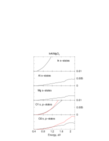
However, accurate electronic band structure investigations for InGaZnO4, =1, showed JEM that the atoms from both InO1.5 and GaZnO2.5 layers give comparable contributions to the conduction band, Fig. 2(a). This resulted in a three-dimensional distribution of the charge density: the interatomic (or “background”) electron density is similar in and across the [0001] layers. The isotropy of the electronic properties in this layered compound manifests itself in the electron effective masses being nearly the same in all crystallographic directions (Table 2).
| Compound | N1 | N2 | Eg(0) | m[100] | m[010] | m[001] | mab | mz |
|---|---|---|---|---|---|---|---|---|
| InGaZnO4 | 48% | 52% | 1.30 | 0.23 | 0.22 | 0.20 | 0.23 | 0.23 |
| InGaMgO4 | 58% | 42% | 2.15 | 0.27 | 0.27 | 0.24 | 0.28 | 0.29 |
| ScGaZnO4 | 26% | 74% | 2.48 | 0.33 | 0.33 | 0.34 | 0.33 | 0.53 |
| InAlMgO4 | 72% | 28% | 2.78 | 0.32 | 0.31 | 0.35 | 0.31 | 0.34 |
Most strikingly, we found that the effective mass remains isotropic when the cation(s) in InGaZnO4 are replaced by other elements with electronic configuration, for example, Sc, Al and/or Mg. This finding may seem to be counterintuitive, since the -states of Sc, Al and Mg are expected to be located deeper in the conduction band due to significantly larger band gaps in Sc2O3, Al2O3 and MgO as compared to those in In2O3, Ga2O3 and ZnO. Analysis of the partial density of states shows that although the contributions from the Sc, Al and Mg atoms to the bottom of the conduction band are notably reduced, cf., Fig. 2 and Table 2, the states of these atoms are still available for the electron transport. Consequently, the interatomic charge density distribution is three-dimensional for all these layered multi-cation oxides – in accord with the isotropic electron effective mass. Moreover, we found JEM that the electron effective mass in these complex materials can be predicted via simple averaging over those of the corresponding single-cation oxides (Table 2).
It is important to stress that the isotropic character of the intrinsic transport properties in the TCO hosts with layered structure may not be maintained when extra carriers are introduced. Different valence states (In3+ and Ga3+ vs Zn2+) and oxygen coordination (octahedral for In vs tetrahedral for Ga and Zn) are likely to result in preferential (non-uniform) arrangement of aliovalent substitutional dopants or oxygen vacancies. We believe that the observed anisotropic conductivity thermoelectr ; Hiramatsu as well as its dependence on the octahedral site density Freeman ; Mason-review in the layered TCO’s is a manifestation of a specific carrier generation mechanism. While proper doping can help make either or both structurally distinct layers conducting, leading to a highly anisotropic or three-dimensional electron mobility, respectively, amorphous complex oxides PhilMag ; Nature ; a-mass readily offer a way to maintain isotropic transport properties.
Thus, we believe that other cations with electronic configuration, beyond the traditional In, Sn, Zn and Cd, can be effectively incorporated into novel complex multicomponent TCO hosts – such as the layered materials decribed above, ordered ternary oxides Mason-review ; Minami ; Minami05 , solid solutions Freeman as well as their amorphous counterparts Minami05 ; PhilMag , important for flexible electronics technologies Nature . Significantly, the sensitivity of the bandgap value to the composition of a multicomponent oxide (Table 2) offers a possibility to manipulate the optical properties as well as the band offsets (work functions) via proper composition of an application-specific TCO.
Finally, it should be mentioned, that the efficient doping of the wide-bandgap oxides is known to be a challenge Neumark ; VandeWalle ; Zunger . Alternative carrier generation mechanisms, for example, magnetic dopants discussed above, introduction of hydrogen ValleNature or ultraviolet irradiation in nanoporous calcium aluminate EPL ; mayenite ; PRLmay , are being actively sought and have already yielded promising results – as outlined in the following section.
.3 Novel UV-activated transparent conductors
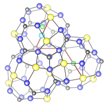
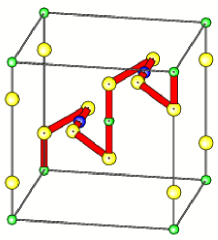
Cage-structured insulating calcium-aluminum oxide, 12CaO7Al2O3, or mayenite, differs essentially from the conventional TCO’s not only by its chemical and structural properties but also by the carrier generation mechanism: a persistent conductivity (with a ten-order of magnitude change) has been achieved upon doping with hydrogen followed by UV irradiation mayenite ; PRLmay .
Mayenite belongs to the CaO-Al2O3 family of Portland cements which are known for their superior refractory properties. The unique structural features of mayenite, Fig. 3, namely, the encaged “excess” oxygen ions, allow incorporation of hydrogen according to the chemical reaction: O2-(cage) + H2(atm.) OH-(cage) + H-(another cage). While the H-doped mayenite remains insulating (Fig. 4(a)), the conductivity results from the electrons excited by UV irradiation off the H- ions into the conduction band formed from Ca -states. The charge transport occurs by electron hopping through the encaged “defects” – the H0 and OH- located inside the large (more than 5.6 Å in diameter) structural cavities. Understanding of the conduction mechanism on the microscopic level PRLmay ; electride resulted in prediction of ways to control the conductivity by targeting the particular atoms that participate in the hopping. These predictions have been confirmed experimentally PRLmay ; Bertoni .


The low conductivity in H-doped UV-irradiated mayenite (1 S/cm, Ref. mayenite ; PRLmay ) was attributed to the strong Coulomb interactions between the UV released electrons which migrate along a narrow conducting channel – the hopping path, Fig. 3. Alleviation of the electronic repulsion electride resulted in the observed Matsuishi2003 100-fold enhancement of the conductivity in the mayenite-based oxide, [Ca12Al14O32]2+(2e-), although the carrier concentration was only two times larger than that in the H-doped UV-irradiated Ca12Al14O33. The improved conductivity, however, came at the cost of greatly increased absorption electride ; Matsuishi2003 due to an increased density of states at the Fermi level, making this oxide unsuitable for practical use as a transparent conducting material.
Despite the failure to combine effectively the optical transparency and with useful electrical conductivity in Ca12Al14O33, the band structure analysis of the mayenite-based oxides suggests that these materials belong to a conceptually new class of transparent conductors where a significant correlation between their structural peculiarities and electronic and optical properties allows achieving good conductivity without compromising their optical properties. In striking contrast to the conventional TCO’s, where there is a trade-off between optical absorption and conductivity, as discussed above, nanoporous materials allow a possibility to combine 100% optical transparency with high electrical conductivity. The schematic band structure of such an “ideal” TCO is shown in Fig. 5. Introduction of a deep impurity band in the bandgap of an insulating material would help to keep intense interband transitions (from the valence band to the impurity band and from the impurity band to the conduction band) above the visible range. This requires the band gap of a host material to be more than 6.2 eV. Furthermore, the impurity band should be narrow enough (less than 1.8 eV) to keep intraband transitions (as well as the plasma frequency) below the visible range.
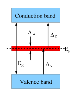
In order to achieve high conductivity, the concentration of impurities should be large enough so that their electronic wavefunctions overlap and form an impurity band. The formation of the band would lead to a high carrier mobility due to the extended nature of these states resulting in a relatively low scattering. For this, a material with a close-packed structure should not be used, because large concentration of impurities would result in (i) an increase of ionized impurity scattering which limits electron transport; and (ii) a large relaxation of the host material, affecting its electronic structure and, most likely, decreasing the desired optical transparency. Therefore, an introduction of a deep impurity band into a wide-band insulator with a close-packed structure would make the material neither conducting nor transparent. Alternatively, materials with a nanoporous structure may offer a way to incorporate a large concentration of impurities without any significant changes in the band structure of the host material. Zeolites have been proposed EPL as potential candidates for the “ideal” TCO’s because they possess the desired structural and optical features, i.e., spacious interconnected pores and large bandgaps, and also exhibit the ability to trap functional “guest” atoms inside the nanometersized cavities which would govern the transport properties of the material.
Thus, understanding the principles of the conventional transparent conductors provide a solid base for further search of novel TCO host materials as well as efficient carrier generation mechanisms. Ab-initio density-functional band structure investigations methods are valuable not only in providing a thorough insight into the TCO basics but also in predicting hidden capabilities of the materials beyond the traditionally employed.
References
- (1) A.J. Freeman, K.R. Poeppelmeier, T.O. Mason, R.P.H. Chang, T.J. Marks, MRS Bull. 25, 45 (2000)
- (2) O.N. Mryasov, A.J. Freeman, Phys. Rev. B 64, 233111 (2001)
- (3) R. Asahi, A. Wang, J.R. Babcock, N.L. Edleman, A.W. Metz, M.A. Lane, V.P. Dravid, C.R. Kannewurf, A.J. Freeman, T.J. Marks, Thin Solid Films 411, 101 (2002)
- (4) H. Mizoguchi, P.M. Woodward, Chem. Mater. 16 5233 (2004)
- (5) J.E. Medvedeva, A.J. Freeman, Europhys. Lett. 69, 583 (2005)
- (6) S. Jin, Y. Yang, J.E. Medvedeva, J.R. Ireland, A.W. Metz, J. Ni, C.R. Kannewurf, A.J. Freeman, T.J. Marks J. Amer. Chem. Soc. 126, 13787 (2004)
- (7) Y. Yang, S. Jin, J.E. Medvedeva, J.R. Ireland, A.W. Metz, J. Ni, M.C. Hersam, A.J. Freeman, T.J. Marks, J. Amer. Chem. Soc. 127, 8796 (2005)
- (8) J.E. Medvedeva, Phys. Rev. Lett. 97, 086401 (2006)
- (9) We note that in Sn-doped In2O3 (ITO) the second, or so-called hybridization gap which was argued to be one of the reasons of low optical absorption in ITO Freeman ; Mryasov closes upon structural relaxation, i.e., when the Sn-O and In-O distances are optimized.
- (10) J.R. Bellingham, W.A. Phillips, C.J. Adkins, J. Mater. Science Let. 11, 263 (1992)
- (11) T.J. Coutts, D.L. Young, and X. Li, Mater. Res. Bull. 25, 58 (2000)
- (12) Y. Meng, X. Yang, H. Chen, J. Shen, Y. Jiang, Z. Zhang, and Z. Hua, Thin Solid Films 394, 219 (2001); J. Vac. Sci. Technol. A 20, 288 (2002)
- (13) Y. Yoshida, T.A. Gessert, C.L. Perkins, and T.J. Coutts, J. Vac. Sci. Technol. A 21, 1092 (2003); C. Warmsingh, Y. Yoshida, D.W. Readey, C.W. Teplin, J.D. Perkins, P.A. Parilla, L.M. Gedvilas, B.M. Keyes, and D.S. Ginley, J. Appl. Phys. 95, 3831 (2004)
- (14) Y. Yoshida, D.M. Wood, T.A. Gessert, and T.J. Coutts, Appl. Phys. Lett. 84, 2097 (2004)
- (15) S. Sun, J. Huang, D. Lii, J. Vac. Sci. Technol. A 22, 1235 (2004); S. Sun, J. Huang, D. Lii, J. Mater. Res., 20, 247 (2005)
- (16) I. Hamberg, C.G. Granqvist, K.F. Berggren, B.E. Sernelius, and L. Engström, Phys. Rev. B 30, 3240 (1984)
- (17) H. Kawazoe, N. Ueda, H. Un’no, T. Omata, H. Hosono, H. Tanoue, J. Appl. Phys. 76, 7935 (1994)
- (18) M. Orita, M. Takeuchi, H. Sakai, H. Tanji, Jpn. J. Appl. Phys. 34, L1550 (1995)
- (19) M. Orita, H. Tanji, M. Mizuno, H. Adachi, T. Tanaka, Phys. Rev. B 61, 1811 (2000)
- (20) H. Kaga, R. Asahi, T. Tani, Jpn. J. Appl. Phys. 43 7133 (2004)
- (21) H. Hiramatsu, H. Ohta, W.S. Seo, and K.J. Koumoto, J. Jpn. Soc. Powder Powder Metall. 44, 44 (1997)
- (22) M. Orita, H. Ohta, M. Hirano, S. Narushima, H. Hosono, Phil. Mag. B 81, 501 (2001)
- (23) K. Nomura, H. Ohta, K. Ueda, T. Kamiya, M. Hirano, H. Hosono, Science 300, 1269 (2003)
- (24) K. Nomura, H. Ohta, A. Takagi, T. Kamiya, M. Hirano, H. Hosono, Nature 432, 488 (2004)
- (25) A. Takagi, K. Nomura, H. Ohta, H. Yanagi, T. Kamiya, M. Hirano, H. Hosono, Thin Solid Films 486, 38 (2005)
- (26) Von K. Kato, I. Kawada, N. Kimizuka, T. Katsura, Z. Krist. 141, 314 (1975)
- (27) N. Kimizuka, T. Mohri, J. Solid State Chem. 60, 382 (1985)
- (28) N. Kimizuka, T. Mohri, J. Solid State Chem. 78, 98 (1989)
- (29) R.D. Shannon, J.L. Gillson, R.J. Bouchard, J. Phys. Chem. Solids 38, 877 (1977)
- (30) H. Kawazoe, K. Ueda, J. Amer. Ceram. Soc. 82, 3330 (1999)
- (31) H. Kawazoe, H. Yanagi, K. Ueda, H. Hosono, MRS Bull. 25, 28 (2000)
- (32) B.J. Ingram, G.B. Gonzalez, D.R. Kammler, M.I. Bertoni, T.O. Mason, J. Electroceram. 13, 167 (2004)
- (33) J.E. Medvedeva, unpublished.
- (34) T. Minami, J. Vac. Sci. Technol. A 17, 1765 (1999); T. Minami, MRS Bull. 25, 38 (2000)
- (35) T. Minami, Semicond. Sci. Tech. 20, S35 (2005)
- (36) G.F. Neumark, Mater. Sci. Eng. R 21, 1 (1997)
- (37) C.G. Van de Walle, Phys. Stat. Solidi B 229, 221 (2002)
- (38) A. Zunger, Appl. Phys. Lett. 83, 57 (2003)
- (39) C.G. Van de Walle, J. Neugebauer, Nature 423, 626 (2003)
- (40) K. Hayashi, S. Matsuishi, T. Kamiya, M. Hirano, H. Hosono, Nature 419, 462 (2002)
- (41) J.E. Medvedeva, A.J. Freeman, M.I. Bertoni, T.O. Mason, Phys. Rev. Lett. 93, 16408 (2004)
- (42) J.E. Medvedeva, A.J. Freeman, Appl. Phys. Lett. 85, 955 (2004)
- (43) M.I. Bertoni, T.O. Mason, J.E. Medvedeva, A.J. Freeman, K.R. Poeppelmeier, B. Delley, J. Appl. Phys. 97, 103713 (2005)
- (44) S. Matsuishi, Y. Toda, M. Miyakawa, K. Hayashi, T. Kamiya, M. Hirano, I. Tanaka, H. Hosono, Science 301, 626 (2003)
- (45) We employed highly-precise all-electron full-potential linearized augmented plane wave (FLAPW) method FLAPW ; FLAPW1 with the local density approximation for the electronic band structure investigations of Mo-doped In2O3, multicomponent O4 compounds, H-doped Ca12Al14O33 and oxygen deficient [Ca12Al14O32]2+(2e-). Each structure has been optimized via the total energy and atomic forces minimization. During the optimization, all atoms were allowed to move along , , and directions while the lattice parameters were fixed at the corresponding experimental values. The UV-irradiated H-bearing Ca12Al14O33 was investigated within the linear muffin-tin orbital method (LMTO) in the atomic sphere approximation LMTO .
- (46) E. Wimmer, H. Krakauer, M. Weinert, A.J. Freeman, Phys. Rev. B 24, 864 (1981)
- (47) M. Weinert, E. Wimmer, A.J. Freeman, Phys. Rev. B 26, 4571 (1982)
- (48) O. K. Andersen, O. Jepsen, M. Sob, Electronic Band Structure and its Applications, (ed. M. Yussouff. Springer-Verlag, Berlin, 1986).