Counting and manipulating single electrons using a carbon nanotube transistor
Abstract
We report on the electric measurements of an individual Au nanoparticle with an ultra-high contact resistance of about . The high-impedance measurements have been carried out by counting the electrons that are transferred onto the particle. In order to do this, a carbon nanotube is used as the electrode for the supply of electrons but also as the detector of the charge transfer. Measurements using single-electron detection allow us to determine the separation between the electron states in the Au nanoparticle, which is about 4 meV, consistent with the charging energy of the particle. Single-electron detection with nanotubes offers great promise for the study of electron transfer in highly resistive molecular systems.
pacs:
73.63.Fg, 73.23.Hk, 73.40.Cg, 73.43.FjDetection and manipulation of individual electron charges are among the ultimate goals of nanoscale electronics. It holds promise for ultra-low dissipative circuits as well as for information processing in highly-resistive molecular circuits. Carbon nanotube transistors tans ; martel offer unique opportunities for single-electron detection. Nanotubes have ultra-small cross-sections and their conducting electrons are located at the tube surface. These advantages have been exploited for the sensing of chemical gas Kong2 ; Collins and biological probes besteman ; Star . Nanotubes have also been used to detect packets of multiple electrons transferred from the nanotube onto a particle, though the precise number of electrons in the packet could not be measured marty . Single-electron detection has been resolved for electrons hopping onto defects randomly trapped in the substrate liu ; ishigami ; lin ; Durkop ; peng . These single-electron processes remain however poorly controlled. Different defects can be probed in parallel, which makes it difficult to assign different electron states to a same defect. As a result, electron properties of such devices can only be partially characterized.
In this letter, we demonstrate for the first time single-electron detection on a nanosystem that is not a defect liu ; ishigami ; lin ; Durkop ; peng , namely a gold nanoparticle. This well-defined device allows for the access of dozens of electron states of the particle, but also for the full electron characterization of the device. In contrast with previous works marty ; liu ; ishigami ; lin ; Durkop ; peng , we can determine the energy separation between the electron states, which is found to be meV, consistent with the charging energy of the particle. We can also determine the resistance between the particle and the nanotube, which is about and results in a transfer rate as low as s-1. Such a low transfer rate, together with the well-defined device, allow us to inject and extract different electrons from the particle in out-of-equilibrium conditions, and to monitor the electron number decay in time.
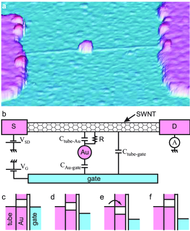
Carbon nanotube transistors are fabricated by means of standard nanofabrication techniques. Tubes are grown by chemical vapor deposition kong on a doped Si wafer with a 1 m thermal silicon oxide layer. They are electrically contacted to Cr/Au electrodes patterned by electron-beam lithography. Gold nanoparticles are deposited onto the wafer from a suspension in water that consists of gold chloride and trisodium citrate. A nm diameter particle is positioned on top of the tube by atomic force microscopy manipulation (Fig. 1 (a,b)).
The transfer of electrons onto the particle can be detected by measuring the conductance of the nanotube while sweeping the gate voltage (Fig. 2(a)), as the tube conductance is extremely sensitive to the presence of electric charges. As is swept from -4 to -1 V, the conductance is turned off as for typical p-doped semiconducting SWNTs tans ; martel . Moreover, we have observed 35 abrupt conductance jumps (vertical red bars) that indicate discrete electron transfers from the nanotube into the particle. Each extra electron in the particle changes the electrostatic potential in the particle and, in turn, the charge density in the nanotube, which shifts the conductance horizontally in .
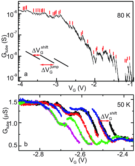
As the measurement is repeated, conductance jumps appear at different gate voltages, see Fig. 2(b). This indicates that electron transfers occur stochastically in time; see also below. Remarkably, repeated measurements fall on curves that are periodically spaced in gate voltage with a period of about 60 mV. The same spacing is observed at all the ’s from the on- to the off-conductance (from -4 to -1 V; see Fig. 2(a)). This periodicity suggests that adjacent curves differ by one electron in the Au particle, and, in turn, that the observed jumps correspond to transfers of single electrons. Measurements on a second device yield a period of about 40 mV.
Measurements on devices without an Au particle look very different. Most often, no conductance jumps are observed at all. For some devices, jumps can be detected, but their number remains very low, and no period in gate voltage can be assigned. Those jumps are attributed to uncontrolled charge traps at defects.
The mechanism that controls electron transfer onto the particle has a lot in common with what happens in a single electron transistor sohn . Adding an electron to the particle costs the Coulomb charging energy (represented by a gap in Fig. 1(c)). By reducing the gate potential , the potential of the Au particle goes down according to Kirchhoff’s laws (Fig. 1(d)). This is described by the first term in
| (1) |
When the tube’s electrochemical potential matches the upper energy of the Coulomb gap in the particle (Fig. 1(e)), an electron can be transferred from the tube onto the particle, and the electron number in the particle is increased by one. This shifts by the amount (Fig. 1(f)), which blocks the transfer of the next electron. In contrast to previous single electron transistors sohn , the transfer rate is slow enough to prevent the last electron from tunnelling out from the particle by continuously sweeping down the gate potential.
We will now look at the time dependence of the electron transfers. For this purpose, the gate voltage is set at a fixed value while measuring the tube conductance, Fig. 3. At 50 K, the tube conductance fluctuates between two values on a time scale of several hundred seconds. We attribute the two level fluctuations to an electron going back and forth into the Au particle due to thermal excitation, and thus changing the number of electrons between and . As the temperature is increased to 150 K, the tube conductance fluctuates between three levels, i.e. between , , and (Fig. 3(b)). The mechanism is schematized in the insets of Fig. 3.
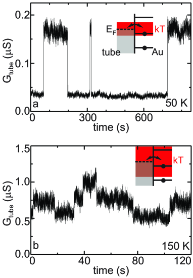
The fluctuations of due to thermal excitation provide information on the energy separation between electron states of the Au particle. The two level fluctuations at 50 K suggest that is about , i.e. meV (see inset of Fig. 3(a)). Taking K gives aF, which is reasonable when considering that the self-capacitance of a sphere aF with and nm has the same order of magnitude.
We will now exploit the low rate of the charge transfer in order to manipulate the number of electrons on the particle in out-of-equilibrium conditions. In order to do this, the gate voltage is rapidly swept to change the potential of the Au particle, which positions different empty (occupied) electron levels of the Au particle below (above) the Fermi energy (schematic of Fig. 4(a)). The number of empty levels depends on the amplitude of the gate voltage sweep. Measuring the tube conductance versus time allows us to monitor the decay towards equilibrium of the electron system (Fig. 4(a)). As discussed previously, each conductance jump corresponds to the transfer of one electron.
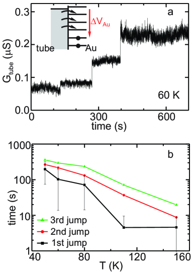
The transfer rate changes as the temperature varies (Fig. 4(b)). The average time for the 3 jumps in Fig. 4(a) is shown to increase dramatically as the temperature is reduced. This suggests that the transfer is not a simple tunnel effect, but that transferred electrons may interact with phonons or other electrons. In principle, such transfer rate measurements can allow us to distinguish between thermally activated and Luttinger liquid-like (power law dependence) behaviours of electrons in the nanotube bockrath ; yao ; gao . The origin of the temperature dependence, however, is beyond the scope of this paper and will be left for further studies.
The measurements above allow us to estimate the electron resistance between the Au particle and the nanotube. The average jump time is
| (2) |
This relation can be seen as the resistance given by the voltage divided by the current . Since , we get at 50 K when s. Such a resistance is six orders of magnitude higher than what conventional electronics can cover. The resistance may originate from a gap of a few nm’s between the tube and the particle or from adsorbate layers at the tube-particle interface. This resistance could not be measured in previous single-electron detection experiments with nanotubes marty ; liu ; ishigami ; lin ; Durkop ; peng .
The device can be further characterized by considering the electric circuit in Fig. 1(b). This circuit has been analyzed for silicon single electron memory using a small floating gate, which represents the ultimate miniaturization of a flash memory Yano ; Durkop . In this model, the conductance jumps in Fig. 2(a) are on average separated by and the adjacent curves in Fig. 2(b) by with
| (3) |
By taking the mean value for mV, mV, and meV, we get aF, aF, and aF. Those values are reasonable considering the device geometry. Indeed, can be roughly estimated by half the capacitance between two concentric spheres, which is aF with being the oxide thickness. is expected to be slightly less than half the capacitance between two coaxial cylinders, which is aF with being the tube length.
The capacitance quantifies the coupling between the Au particle and the gate. , which is 1.8 aF, is remarkably large when considering that the gate is 1 m away from the Au particle. Compared to previous experiments on Au particles directly contacted to metal electrodes, the same coupling can be achieved provided that the separation between the gate and the Au particle is reduced to 2-3 nm Magnus ; Bolotin . This is because most of the electric field in the latter case is screened by the metal electrodes. Overall, our device layout enables an efficient coupling, which allows access to a broad range of energy levels by sweeping the gate voltage. This is especially interesting for future studies on organic and biological molecules, since the large energy separation between the levels has often limited access to only one level Park ; Liang .
We will now compare our work to other existing single-electron detectors, which are devices microfabricated in metal or semiconducting material working at millikelvin temperatures lu ; Elzerman ; bylander ; gustavsson ; fujisawa . The operation temperature (up to 150 K) of nanotube detectors is much higher. In addition, nanotubes are suitable for electron detection on systems that are physically different from the detector itself, such as molecules or nanoparticles. In contrast, microfabricated single-electron detectors so far have only probed systems structured in the same semiconducting or metal material than the detector. Moreover, these detectors are much larger in size, which is unpractical for addressing molecules.
In conclusion, single-electron detection with a nanotube transistor has been used to electrically probe a gold nanoparticle with an ultra-high contact resistance of about . This is remarkable, since such a resistance is six orders of magnitude higher than what conventional electronics can cover. We have shown how single-electron detection with nanotubes can be used to extract important information about the Au particle, such as the energy separation between the electron states. Single-electron counting with nanotubes offers great promise for future studies on organic molecules, biomolecules, or semiconducting particles, which most often are highly resistive. Interestingly, electron states of those systems are expected to depend not only on the charging energy, but also on the molecular levels. Single-electron photoelectric effects can also be investigated, for instance, in CdSe particles Gudiksen as well as charge transfer in biomolecules involved in photosynthesis and respiration activities Gray . This technique may also provide information on internal electron transfer events that occur within complex molecular systems.
We thank P. Gambardella, B. Placais, S. Sapmaz and P. Gorostiza for discussions. The research has been supported by an EURYI grant and the EU funded project CARDEQ (FP6-IST-021285-2).
∗ corresponding author: adrian.bachtold@cnm.es
References
- (1) S. J. Tans, A. R. M. Verschueren, C. Dekker, Nature 393, 49 (1998).
- (2) R. Martel , Appl. Phys. Lett. 73, 2447 (1998).
- (3) J Kong,et al., Science 287, 622 (2000).
- (4) P.G. Collins, K. Bradley, M. Ishigami, A. Zettl, Science 287, 1801 (2000).
- (5) K. Besteman, et al., Nano Lett. 3, 727 (2003).
- (6) A. Star, J.C.P. Gabriel, K. Bradley, G. Gruner, Nano Lett. 3, 459 (2003).
- (7) L. Marty, et al., Small 2, 110 (2006).
- (8) F. Liu , Appl. Phys. Lett. 86, 163102 (2005).
- (9) M. Ishigami , Appl. Phys. Lett. 88, 203116 (2006).
- (10) Y.M. Lin, et al., Nano Lett. 6, 930 (2006).
- (11) T. Durkop, B. M. Kim, and M. S Fuhrer, J. Phys.: Condens. Matter 16, R553 (2004).
- (12) H.B. Peng, M.E. Hughes, J.A. Golovchenko, Appl. Phys. Lett. 89, 243502 (2006).
- (13) J. Kong, et al., Nature 395, 878 (1998).
- (14) Sohn, L.L., Kouwenhoven, L.P. & Schon, G. Mesoscopic Electron Transport (Kluwer, Dordrecht, 1997).
- (15) M. Bockrath, et al., Nature 397, 598 (1999).
- (16) Z. Yao, H.W.Ch. Postma, L. Balents, C. Dekker, Nature 402, 273 (1999).
- (17) B. Gao, et al., Phys. Rev. Lett. 92, 216804 (2004).
- (18) K. Yano, et al., Proc. IEEE 87, 633 (1999).
- (19) S.H. Magnus Persson, L. Olofsson, L. Gunnarsson, Appl. Phys. Lett. 74, 2546 (1999).
- (20) K.I. Bolotin, F. Kuemmeth, A.N. Pasupathy, D.C. Ralph, Appl. Phys. Lett. 84, 3154 (2004).
- (21) J. Park, et al., Nature 417, 722 (2002).
- (22) W. Liang, et al., Nature 417, 725 (2002).
- (23) W. Lu, et al., Nature 423, 422 (2003).
- (24) J.M. Elzerman, et al.,Nature 430, 431 (2004).
- (25) J. Bylander, T. Duty, and P. Delsing, Nature 434, 361 (2005).
- (26) S. Gustavsson, et al., Phys. Rev. Lett. 96, 076605 (2006).
- (27) T. Fujisawa, T. Hayashi, R. Tomita, Y. Hirayama, Science 312, 1634 (2006).
- (28) M.S. Gudiksen, K.N. Maher, L. Ouyang, H. Park, Nano Lett. 5, 2257 (2005).
- (29) H.B. Gray, J.R. Winkler, Proc. Natl. Acad. Sci. USA 102, 3534 (2005).