Parallel Distribution of Asynchronous Optical Signals
Abstract
An eleven channel digital asynchronous transceiver (DAT) employing parallel optical link technology has been developed for trigger signal distribution across the Very Energetic Radiation Imaging Telescope Array System (VERITAS). Combinatorial logic functions are implemented in Xilinx Spartan 3 FPGAs, providing a versatile solution adaptable for use in future atmospheric Čerenkov detectors and other high-energy astroparticle experiments. The device is dead-time free and introduces a minimal skew of 1.6 ns between channels. The jitter on each DAT channel is less than 0.8 ns 95% of the time, allowing communication between telescopes and a central trigger system separated by hundreds of meters, without limiting array performance.
keywords:
Gamma Ray , PAROLI , VCSEL , Čerenkov , FPGAPACS:
29.90.+r , 42.55.Wd , 95.55.Ka , 95.75.Tv, , ,
1 Introduction
The Very Energetic Radiation Imaging Telescope Array System (VERITAS) [5] consists of four 12 m diameter atmospheric Čerenkov telescopes equipped with photo-multiplier cameras. The array uses a multi-level trigger system to reject fluctuations in background light whilst efficiently recording signals from gamma-ray initiated air showers. Discriminated photo-multiplier signals are passed to a pattern selection trigger at each telescope [2] resulting in a cosmic ray trigger rate at high telescope pointing elevations of 150 Hz for a discriminator threshold of 6-7 photoelectrons. These decisions are then passed to a central array trigger requiring a multiple telescope coincidence. The array trigger requires the distribution of multiple, fast, digital pulses between telescopes. A versatile solution is essential as not only fast, narrow, trigger signals but also variable width event numbers and long calibration flags must be transmitted.
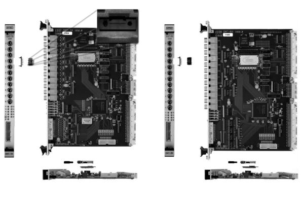
The data from each camera pixel is digitised into 2 ns slices by custom built 500 MHz FADC boards [3]. Upon receiving an array trigger signal the FADC buffers are readout. The trigger signals require nanosecond accuracy to trigger the readout of the FADC modules from the correct point in the buffers. The FADC readout time has a direct effect on the telescope deadtime and energy threshold, so it is important the minimise the readout window around the data pulse. A large amount of jitter in the trigger signal would require a large readout window, increasing the system deadtime and the detector energy threshold. Typically the FADC readout window is set to 24 samples, or 48 ns in VERITAS. Accordingly a Digital Asynchronous Transceiver (DAT) has been developed at the University of Leeds in collaboration with Hytec Electronics Ltd. consisting of a transmitter and a receiver both implemented as single width VME modules, Figure 1. The transmitter and receiver are linked by fibre optic interconnects running between telescopes. Fibre is lighter and less bulky than coaxial cable of the equivalent length and is not susceptible to electromagnetic interference.
2 Specification
The DAT transmitter must accept differential negative emitter coupled logic (NECL) inputs via both an IDC header and twin-axial LEMO connectors before presenting them in an identical form at the receiver outputs. Ideally, the solution should exceed the current trigger requirements and be adaptable for future developments, both within atmospheric Čerenkov astronomy and high energy astrophysics in general.
To minimise the FADC readout window within VERITAS it is desirable to maintain the trigger timing to the level of one FADC sample. The array trigger signal distributed by the DAT modules is based upon telescope level triggers also transmitted over DAT modules and received centrally. The array trigger itself has an RMS jitter of 1 ns, so to keep the total RMS jitter of the array trigger signal below one FADC sample, each channel of a DAT module should have 1 ns RMS jitter. The array trigger system uses a pulse delay module to compensate for the differences in timing introduced by the difference in arrival time of the shower front at the telescopes depending on the observation direction. This method requires the array system signals traverse a path of predictable duration. Therefore a maximum channel-to-channel skew of 2 ns within the DAT modules is desired.
For versatility, the DAT must transport asynchronous pulses of varying width at an undefined frequency such that the same system can be used to distribute housekeeping information111In the case of VERITAS the width is of the order of tens of nanoseconds to milliseconds at frequencies of the order of Hz up to a few MHz.. The system should be deadtime free to remove the possibility of missing incoming pulses whilst the data is being transmitted.
3 Implementation
3.1 Overview
The DAT consists of two, 6U high, single width VME modules denoted DAT-TX and DAT-RX, transmitter and receiver respectively, see Figure 2. As described in Section 3.3, control and monitoring takes place via a VME interface embedded into an onboard Xilinx Spartan 3 XC3S50 Field Programmable Gate Array (FPGA) [18].
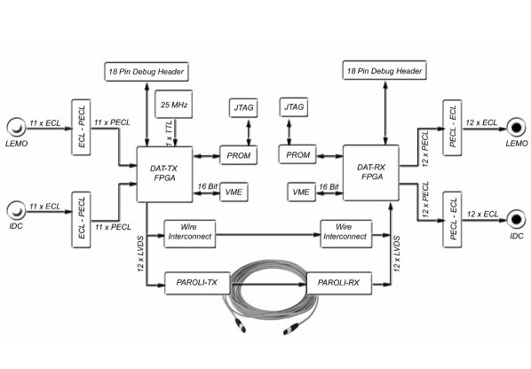
To maintain signal integrity and avoid any lightning induced power surges, which are a hazard with copper cable, a 62.5/125 m core fibre optic interconnect is used to transport signals over the distance of at least 150 m between telescopes. The conversion of electrical signals to optical signals is achieved using the Infineon 1.25 Gbit/s parallel optical link (PAROLI 2® [8], see Figure 1) consisting of a small form factor, 12 channel, 850 nm VCSEL driven transmitter and PIN diode array based receiver. The PAROLI laser devices have a range of around 800 m that puts an upper limit on the distance between DAT modules and therefore telescopes. As a matter of laser safety a given PAROLI transmitter channel will become disabled if a signal exceeds a duty cycle (DC%) of 57% within 1 s. Thus the asynchronous variable width input data signals cannot be sent to the PAROLI directly, they must first be modulated to the DC% requirement in a recoverable manner.
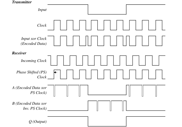
The minimum signal switching time and DC% condition of the PAROLI are satisfied by encoding incoming data signals with a 25 MHz clock through exclusive OR (XOR) gates at the transmitter. The encoded data signals and a copy of the clock are optically transmitted to the receiver where a second set of XOR gates recovers the data. Using this asynchronous, combinatorial method deadtime incursions associated with sequential logic are avoided.
Combinatorial logic is usually implemented in surface mounted, function-specific, IC chips. To accommodate rapid design change (e.g. to optimise the boards for additional applications) and the future possibility of a PAROLI without rigorous duty cycle constraints, all logic is performed within the onboard FPGA. As the gate array is used to implement the VME interface this is an economical solution.
3.2 Physical Description
Differential NECL data enters the front of the DAT-TX via either the 26 way IDC header or the eleven twin-axial LEMO connectors, selectable over the VME interface.
Surface mounted, three channel, MC10EP90 [10] chips convert NECL into low-voltage positive emitter coupled logic (LVPECL) suitable for input to the FPGA. Retaining a differential signal standard improves signal integrity but requires twice as many FPGA input pins. The 25 MHz clock is provided by an onboard TTL oscillator.
The XOR encoded data and clock are output from the FPGA in low voltage differential signal (LVDS) form; the required input to the PAROLI. The PAROLI itself is attached to a daughter board using a 100 pin, ball gate array mounted connector. This configuration would allow the PAROLI to be replaced with a future device by simply redesigning the daughter board. A male MPO terminated 12 channel ribbon-fibre is plugged directly into the PAROLI.
At the receiver the PAROLI converts the incoming optical signals back to LVDS. There is also a 26-way wire interconnect option available to communicate between DAT modules during system debugging. The LVDS signals are then input to the receiver’s Xilinx Spartan 3 where the data is recovered.
Recovered data lines are output from the FPGA as LVPECL and converted with three channel MC100EL91 [11] chips to NECL. The eleven data signals and clock signal are presented on the front panel to both twin-axial LEMO connectors and a 26 way IDC header.
Upon power-up the FPGA on each module is programmed from a socket mounted Atmel AT17LV512 EePROM [1] via jumper selection. In the absence of a PROM programming can be done via a JTAG header. This setup provides the most versatile programming architecture, allowing the user to reprogram the FPGA in seconds over the JTAG connection when testing modifications to the modules.
3.3 FPGA Combinatorial Encoding and Decoding
The embedded VME interface register set provides 16 bit access to three registers. The first two registers simply read the module model number and ID. The third acts as a control status register (CSR) and allows the user to control and monitor the modules. The CSR can enable and disable the laser used in the PAROLI and the clock used in the XOR encoding. The transmitter input choice of IDC header or twin-axial LEMO connector is also set using the CSR, and a user LED on the front panel may be controlled for diagnostic purposes. A test header on the boards may be enabled to input and output 7 additional signals to the FPGA. These pins may be assigned a function and signal standard by reprogramming the FPGA. A simple C++ program scans the VME crate and records the slot numbers of all DAT modules present, identifying them as either transmitter or receiver. The user may then select a given module to access the CSR. Automated programs scan and start up or shut down all the modules in a crate, enabling or disabling the laser and clock, and setting the LVDS inputs via a configuration file or, in the case of VERITAS, a database table. At present the status of transmitted data may not be monitored over the VME interface, and equally data pulses may not be injected in this way. Whilst this functionality is straightforward to implement tests showed that changing the FPGA code to intercept the data paths effected the timing of the signals which, as described later in this section, is crucial to the correct recovery of the data. Further VME functionality is desirable in any future iterations.
At the transmitter, the 22 differential LVPECL signals from both the twin-axial and IDC inputs are buffered onto the FPGA. Each input is selected individually over VME via multiplexers within the gate array. The 25 MHz clock is input via a dedicated clock-buffer to a low skew network on the FPGA and fanned out 12 times. Each of the fanned out clocks enters an XOR gate with a corresponding data line, except for the twelfth clock which enters an XOR gate with ground to maintain duty cycle and transit time. The eleven encoded data lines and clock encoded with ground are buffered to differential outputs on the FPGA. During laboratory tests the duty cycle of the encoded transmitter output was seen to vary by around 0.5% (200 ps) from a low input data state to a high input data state. This duty cycle dependence on the high/low state of the input is attributed to rising and falling signal edges taking different paths through the FPGA, leading to unequal transition times.
At the receiver the differential clock is buffered to a digital clock manager (DCM). Feedback into the DCM facilitates a phase shift between the input and output with a resolution of 156 ps for a 25 MHz clock. The phase shifted clock is fanned out and entered along with the 11 data lines to XOR gates. As previously noted, the duty cycle of the encoded signal exiting the transmitter and arriving at the receiver depends on whether the input to the transmitter is high or low. Due to this duty cycle dependence on the high/low state of the input it is not possible to phase shift the clock to a point where the input is accurately reproduced for both high and low input states. Instead the clock is phase shifted to a position where the output accurately represents the input during a low state. During a high state the output shows sharp spikes down to the low state. Thus for transmitter input as shown in Figure 3 the result A is obtained. To remedy this, an inverted copy of the phase shifted clock is XOR combined with a second copy of the data to produce the result B. The results A and B are used to clock a dual data rate flip-flop at the output stage to reproduce the data, Q. The behaviour of the flip-flop is given by the simple rules in Table 1.
4 Performance
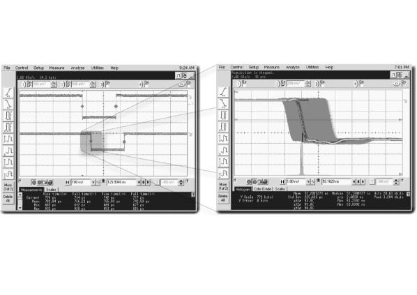
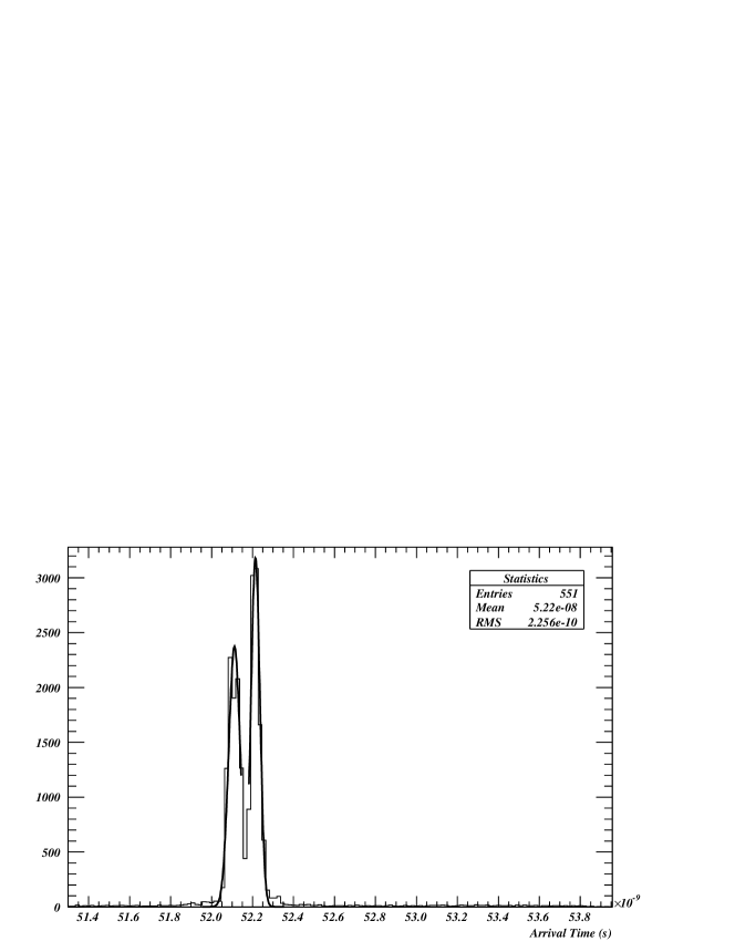
To characterise the performance of the DAT modules the arrival time of the falling edge of a periodic, 1 MHz, 200 ns wide input to the transmitter is measured at the receiver output, relative to the falling edge of a reference pulse as shown in Figure 4. The arrival time varies about some mean for a given channel. The maximum difference between the mean values of the 11 channels is the skew. The variance in arrival times over many measurements for a given channel is the jitter. The skew and average jitter over all channels are taken as the two key indicators of performance.
The term jitter simply refers to the uncertainty of a data edge in time. There are several methods of measuring the jitter. The chosen method here is to use an oscilloscope to record the arrival time of the edge many times and add these values to a histogram. The jitter on each channel is obtained from the distribution of around 20 k measurements over a 2 m long, MPO terminated, 12 channel fibre ribbon cable, as shown in Figure 5.
As the distribution of arrival times at the DAT output is not purely Gaussian one cannot simply equate the jitter to the of the distribution [4, 12]. The total jitter is instead a combination of two principle components: random jitter, , and deterministic jitter, .
Random jitter is uncorrelated and unbounded. Given enough data samples random jitter will have an unlimited peak-to-peak value. For this reason is measured in terms of the standard deviation, . The probability distribution function of random jitter is always Gaussian. is often caused by thermal noise in decision circuits and oscillator phase noise. The number of recorded data samples is depends upon the probability for a logic transition fluctuating across the sampling point, known as the bit error rate, . The random jitter for a given is related to the quantity , a multiple of the standard deviation of the Gaussian, by Eq. 1.
| (1) |
Deterministic jitter is bounded and always measured in terms of a peak-to-peak value. The distribution of deterministic jitter can be very unpredictable. The total jitter, for a given BER is given by the summation of and as shown in Eq. 2.
| (2) |
The deterministic and random jitter may be separated from the recorded distribution via the dual-Dirac model and used to predict a total jitter for the industry standard BER of (which corresponds to ) [16, 15, 13]. In the dual-Dirac method the recorded distribution is modelled by two delta functions displaced in time and convolved with a Gaussian. The standard deviation of this Gaussian, , is estimated by fitting the outer edges of the measured jitter distribution. The displacement of the delta functions is given by the separation of the outer peaks in the measured jitter distribution, and then taken to be .
The validity of this method was tested in two trials. First an oscilloscope was set to average the waveform over a number of acquisitions; the resulting jitter distribution averages out the deterministic jitter, leaving only random jitter. The standard deviation of this distribution proved consistent with derived from the dual-Dirac method. Secondly the dual-Dirac model was used to estimate for a BER of and compared to the peak-to-peak value of the measured jitter distribution for the same BER. Again the two were found to be consistent. It should be noted that it is not feasible to measure BERs of directly due to the acquisition time required. The results of these trials indicate that a sample of 20 k measurements is enough to adequately determine both and , and therefore extrapolations to higher BERs are valid.
A total jitter of 2.50 ns (or 1.25 ns) peak-to-peak for a BER of is obtained for the channel in the example distribution shown in Figure 4. The measurements for all channels over a 60 m cable are shown in Table 2 and an average total jitter of 2.20 ns (or 1.10 ns) is obtained. This BER extrapolation to 1012 pulses is not intended as a replacement for measurements made on a dedicated BER machine but simply provides a quick estimation of the worst case jitter. The method provides an estimate of the expected performance of a given channel and may be used to rate channels according to performance for use with critical signals within VERITAS. A more practical estimate of the jitter, in the absence of a Gaussian distribution, that will effect the trigger chain on an event-by-event basis is simply the time over which 95% of pulses arrive. On average over all channels, 95% of pulses arrive within 0.570 ns (or 0.265 ns) of the average for that channel. This is crucially less than 1 ns, facilitating the accurate transmission of VERITAS array trigger pulses. Consequently trigger signals arrive at the FADC modules accurately enough to allow the determination of the position of the data in the buffers to within one FADC sample (2 ns), as described in Sections 1 and 2. The skew between output channels from the average arrival times is 1.6 ns (at the 95% confidence level), small enough to integrate into the VERITAS trigger chain without affecting the pre-programmed delays within the array trigger system which compensate for the relative movement of the telescopes.
Since the system introduces no deadtime the minimum pulse width that can accurately be transmitted is only limited by the signal switching speed and the system jitter. The minimum transmittable pulse width is around 5 ns. This is also the time gap required between consecutive pulses, and therefore the maximum transmittable data rate is 200 MHz.
5 Critical Evaluation
The performance of the DAT modules exceeds the requirements of the current VERITAS trigger chain. However, the FPGA code and methodology have proven complicated due to the accuracy required to align the clock with encoded data at the receiver. If the alignment is not correct at the sub-nanosecond level a given channel will produce spurious noise at either the clock frequency (25 MHz) or double the clock frequency (50 MHz). These pulses have a width corresponding directly to the misalignment of the clock and encoded data signal and a minimum width of around 2 ns, the signal switching time at the FPGA output stage. Spurious pulses do not occur at all if a channel is aligned.
The FPGA timing performance is adequate; all signals leaving the transmitter are aligned to within 300 ps, but the duty cycle distortion incurred is disappointing. The PAROLI modules also introduce a 100 ps skew at the transmitter and again at the receiver.
In practice a fibre-ribbon cable must be used to connect the DAT modules to ensure that the 12 fibres are of identical length. Successful alignment over individual fibres is possible and only requires that the fibres are of equal length to within 10 cm. However, we found that when burying cable in 150 m of filled trenches on site this proved challenging. Thus we turned to the fibre-ribbon cable as the only viable outdoor option.
Laboratory tests showed no correlation between variations in either circuit board or fibre temperature and the transit time and jitter of pulses over approximately 10∘C. On site the modules are cooled by fan trays to maintain an approximately constant temperature and therefore the relatively narrow range of temperatures examined in the laboratory is sufficient. The temperature of the fibre-optic cable running between telescopes may experience more significant variations in temperature than measured in the laboratory. The use of 12-channel fibre-ribbon cable ensures that the transit times down both the clock and data channels are effected equally by any extreme temperature variations.
The load stability and the effect of instabilities in the power supply have not been measured. It has been observed that switching modules between VME crates with varying power supplies can affect the timing, even knocking some channels out of alignment. This must be examined further.
6 Conclusion
Fast digital trigger and event number distribution is achieved within VERITAS using FPGA based DAT modules. The modules incorporate PAROLI fibre optic interconnects to protect against lightning induced power surges associated with coaxial cabling and to minimise channel-to-channel skew and jitter. Combinatorial encoding and decoding of the data results in a dead-time free system, and helps to minimise the dead-time of the VERITAS array as a whole. The first stereo data acquired by VERITAS (using two DAT pairs) has been presented elsewhere [6, 7, 9]. The four telescope array requires 8 pairs of modules, all of which are operational as of March 2007. A further 4 DAT pairs are to be supplied as spares by October 2007. The DAT performance is limited by the allowable channel-to-channel skew of the encoded data and clock pulses arriving at the receiver. This currently requires a 12 channel fibre-ribbon cable. Future design changes could correct for this problem by introducing an FPGA with programmable delay on a individual input pins.
This versatile technology could be adopted for other applications such as triggers for particle physics experiments or clock distribution within neutrino telescopes.
Acknowledgements
The authors acknowledge the support of the
VERITAS collaboration and thank all those who helped with the
integration of the DAT modules into the detector. This work was made
possible with the financial support of the White Rose Studentship
programme and PPARC.
References
- [1] Atmel, AT17LV512 EEPROM, Datasheet, Literature Number 2321G-CNFG-7/05, (2005). http://www.atmel.com/literature
- [2] Bradbury S.M. & Rose H.J., Nucl. Instr. & Meth. A, 481, 521, (2002).
- [3] Buckley, J.H., et al., Proc. 28th ICRC, Tsukuba, (2003).
-
[4]
Hancock, J., Identifying Sources of Jitter,
Agilent Technologies, Technical Paper Presented at Euro DesignCon
(2004).
http://www.iec.org/events/2004/euro_designcon. - [5] Holder, J. et al., Astroparticle Physics, 25, 391, (2006).
- [6] Holder, J. et al., VERITAS: Status and Performance, Proceedings of Science with the New Generation of High Energy Gamma-ray Experiments, (2006).
- [7] Huges, S. et al., Initial Stereo Analysis of Mrk 421 from the VERITAS Telescopes, Proceedings of the International School of Cosmic Ray Astrophysics, Erice, (2006).
-
[8]
Infineon Technologies, PAROLI
2®, Preliminary Data Sheet, (2003).
http://www.tranzistoare.ro/datasheets/700/295487_DS.pdf - [9] Krennrich, F. et al., Status Report From VERITAS, Proceedings of the TeV-II Workshop, Wisconsin, (2006).
- [10] Onsemi, MC10EP90 Datasheet Publication Order Number: MC10EP90/D, (2004). http://onsemi.com
- [11] Onsemi, MC100EL91 Datasheet Publication Order Number: MC100EL91/D, (2005). http://onsemi.com
- [12] Papoulis, A., Probability, Random Variables, and Stochastic Processes. New York: McGraw-Hill, (1984).
- [13] Proakis, J.G, Digital Communications, New York: McGraw-Hill, (1995).
- [14] Senior, J.M. Optical Fiber Communications: Principles and Practice (2nd edition), Englewood Cliffs, New Jersey: Prentice Hall, (1992).
- [15] Shanmugan, K. S. and Breipohl, A. M., Random Signals: Detection, Estimation, and Data Analysis, New York: John Wiley and Sons, (1988).
- [16] Stephens, R., Jitter Analysis: The Dual-Dirac Model, RJ/DJ, and Q-Scale, Agilent Technologies Whitepaper 5989-1146EN, (2004).
- [17] Wolaver, D.H., Measure Error Rates Quickly and Accurately, Electronic Design, pp. 89-98, May 30th, (1995).
- [18] Xilinx, Spartan-3 FPGA Family: Complete Data Sheet, Xilinx Literature Number DS099 (v2.1), (2005). http://www.xilinx.com
| A | B | Q |
| X | 1 | |
| X | Q | |
| X | 0 | |
| X | Q |
| Channel | HITS | ||||||||
|---|---|---|---|---|---|---|---|---|---|
| 0 | 346.00 | 2.47 | 0.22 | 20.49 | 0.03 | 0.47 | 2.22 | 2.69 | 1.02 |
| 1 | 344.84 | 1.55 | 0.10 | 20.28 | 0.05 | 0.73 | 1.15 | 1.88 | 0.25 |
| 2 | 344.45 | 1.80 | 0.16 | 20.52 | 0.03 | 0.50 | 1.53 | 2.03 | 0.40 |
| 3 | 344.98 | 1.73 | 0.15 | 20.17 | 0.05 | 0.67 | 1.36 | 2.03 | 0.40 |
| 4 | 345.71 | 1.73 | 0.13 | 24.59 | 0.03 | 0.41 | 1.50 | 1.91 | 0.40 |
| 5 | 345.44 | 1.58 | 0.12 | 20.86 | 0.04 | 0.56 | 1.28 | 1.84 | 0.35 |
| 6 | 345.48 | 1.78 | 0.16 | 20.02 | 0.04 | 0.55 | 1.48 | 2.03 | 0.47 |
| 7 | 345.30 | 2.02 | 0.15 | 20.74 | 0.03 | 0.50 | 1.75 | 2.24 | 0.51 |
| 8 | 345.10 | 1.96 | 0.17 | 20.12 | 0.02 | 0.35 | 1.78 | 2.12 | 0.69 |
| 9 | 345.60 | 3.13 | 0.30 | 20.97 | 0.10 | 1.44 | 2.34 | 3.78 | 1.44 |
| 10 | 345.14 | 1.82 | 0.12 | 20.41 | 0.03 | 0.44 | 1.58 | 2.02 | 0.36 |