Spin-polarized transport in II–VI magnetic resonant tunneling devices
Abstract
We investigate electronic transport through II–VI semiconductor resonant tunneling structures containing diluted magnetic impurities. Due to the exchange interaction between the conduction electrons and the impurities, there arises a giant Zeeman splitting in the presence of a moderately low magnetic field. As a consequence, when the quantum well is magnetically doped the current–voltage characteristics shows two peaks corresponding to transport for each spin channel. This behavior is experimentally observed and can be reproduced with a simple tunneling model. The model thus allows to analyze other configurations. First, we further increase the magnetic field, which leads to a spin polarization of the electronic current injected from the leads, thus giving rise to a relative change in the current amplitude. We demonstrate that the spin polarization in the emitter can be determined from such a change. Furthermore, in the case of a magnetically doped injector our model shows a large increase in peak amplitude and a shift of the resonance to higher voltages as the external field increases. We find that this effect arises from a combination of giant Zeeman splitting, 3-D incident distribution and broad resonance linewidth.
Index Terms:
Spin polarization, tunnel diodes, diluted magnetic semiconductors.I Introduction
Present information processing technology is mostly based on the manipulation of the electron charge by means of external electric fields. In the rapidly flourishing field of spintronics or magnetoelectronics the chief role is played by the electron spin. Spintronics has already provided us with commercial devices, e.g., read-out heads for computer hard disks. These gadgets make use of the giant magnetoresistance effect in metals. In semiconductor materials, the spin orientation of conduction electrons survives much longer time, which makes semiconductor-based spintronic devices, to a great extent, attractive for quantum computing where the electron spin would play the role of a qubit of information [1].
A basic requirement for the applicability of spintronic devices is their all-electrical ability of generating and detecting spin-polarized currents. The most promising prospect devices use alloys of nonmagnetic semiconductors with magnetic transition metals (mainly, Mn) [2]. Thus, thin layers of diluted magnetic semiconductor (DMS) compounds can be stacked to form quantum confined geometries in which new spin-dependent transport effects are likely to occur [3]. Recent progress has been able to reduce Mn-related scattering and, at the same time, maximize spin effects. For example, large band electron spin splittings at moderately low magnetic fields can take place in II–VI compounds (e.g., CdTe, ZnS or ZnSe) with Mn substituted on the group II site [4]. Since the valence of the cations Cd or Zn equals that of Mn, additional n-doping is required to generate electric carriers. The possibility of n-doping is a great advantage of II–VI-based devices over their III-V counterparts (typically, (Ga,Mn)As) which are always p-type, since this difference allows to significantly decrease the amount of spin-orbit coupling experienced by the carriers and, as a result, spin dephasing and relaxation are reduced. Another advantage is related to the spin injection efficiency [5, 6]. The price one has to pay is that n-doped II–VI DMS’s do not show ferromagnetism. Nevertheless, II-VI DMS structures provide an excellent framework for fundamental studies on the dynamical interplay between spin splitting subbands, electron transport, spin decoherence and magnetically controlled quantum confinement.
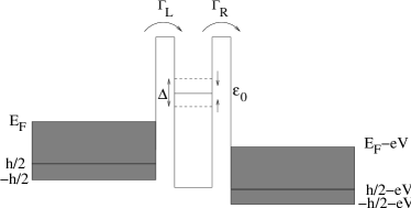
The type of DMS structures with which we are here concerned are resonant tunneling diodes (RTD’s). These systems have recently received attention [7, 8, 9, 10, 11, 12]. A RTD is a widely studied quantum semiconductor device which is the analog of the optical Fabry-Perot resonator [13]. A double barrier confines the electrons in a quantum well between two electron reservoirs. (A simplified sketch of the conduction band profile of a RTD sample is shown in Fig. 1). Resonant tunneling arises when the incident stream of electrons matches its energy with the quantum level formed in the well, thereby working as an energy filter to a good extent. A higher bias lowers the resonance energy relative to the energy of the injected electrons and the current–voltage (–) thus exhibits a negative differential conductance region. This effect can be used for high speed switching applications in electronic circuitry at room temperature [14, 15].
When the quantum well is doped with Mn ions, the resulting DMS is paramagnetic. In the absence of magnetic fields, the well subbands are spin degenerate. When a small magnetic field is applied, a giant Zeeman splitting (of the order of a few meV) arises due to the exchange interaction between the localized magnetic moments (the Mn++ ions) and the conduction band electrons [16]. As a consequence, the bottom of the well energy subbands splits and two conduction channels (one per spin) are able to participate in the transport, see Fig. 1. Using bias voltage to select a particular transmission resonance leads to the generation of a current peak with predominantly spins up or down. Reference [7] showed that each resonance appears as a distinct peak in the – characteristic and that further increase of the magnetic field leads to a larger peak splitting. The separation follows a modified Brillouin function for paramagnetic systems [7],
| (1) |
where is the concentration of Mn spins, is related to the exchange integral (see below), is the Brillouin function with the Landé factor, is the magnetic field, is the temperature, and and are the Mn effective spin and temperature, respectively. Each peak of the splitting is dominated by tunneling via a given spin channel. As a consequence, the RTD works as a spin filter. At large magnetic fields, the splitting reaches saturation but the Zeeman spin splitting in the contacts, which is negligible at low magnetic fields, starts to play a role. The well is progressively injected with an increasing carrier density with a given spin direction and, as a result, the peak amplitude is modified. In this operation regime, we predict that the DMS RTD can be regarded as a detector of spin polarized currents.
When the quantum well is a normal semiconductor and the injector is doped with Mn ions, a different scenario results. The giant Zeeman splitting develops now in the injector, which modifies the energy distribution of the injected current. The calculated – consists of a single peak with an amplitude which enhances largely with increasing magnetic field. Moreover, we observe a shift of the resonance to higher voltages.
Below, we discuss in detail the two predictions sketched above. We present a theoretical model which shows that the effect causing the peak current enhancement in the DMS injector case is due to a combination of three-dimensional incident distribution, giant Zeeman spin splitting and broad resonance linewidth. In the case of a DMS quantum well, we demonstrate that the spin polarization of the emitter can be determined from the relative change of the peaks forming the splitting.
II Experimental sample
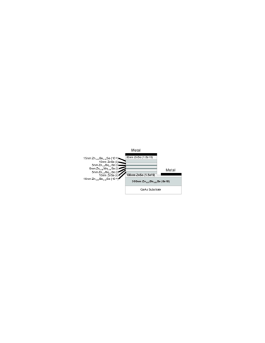
Figure 2 shows a pictorial representation of the sample used in the experiment. The tunneling region consists of a 9 nm thick Zn.96Mn.04Se quantum well sandwiched between two 5 nm thick Zn.7Be.3Se barriers. The well is coupled to two 10 nm thick ZnSe layers. The remaining layers are needed to ensure a proper doping profile and to allow for the fitting of high quality ohmic contacts. The contact resistance of the devices is kept to a minimum by using an in-situ Al (10 nm)/Ti (10 nm)/Au (30 nm) top contact, while the ex-situ bottom contact is fabricated by etching down to the very highly doped ZnSe layer, and using large area (500m Ti-Au contact pad. The injector and the collector are lattice matched to the GaAs substrate. The barrier layers are obviously not lattice matched but are sufficiently thin to grow fully strained. The sample is patterned in 100 m2 pillars using standard optical lithography with positive photoresist followed by metal evaporation and lift-off.
Measurements are performed in a 4He bath cryostat equipped with a high field superconducting magnet using standard DC transport techniques. Care was taken to construct a circuit with a low (40 ) resistor in parallel to the diode to prevent the diode from going into oscillations in the negative differential conductance region. [17]. Current measurements consist of measuring the voltage drop across a relatively small 30 Ohm series resistor.
III Experimental observations
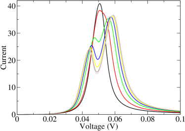
– characteristics for the DMS RTD and different strengths of applied magnetic fields are shown in Fig. 3. At zero field, the sample exhibits typical RTD behavior, showing a strong resonance peak at 51 mV with a peak-to-valley ratio just over 1. The additional resonance visible at 84 mV in the curve is the well known LO phonon replica [17] which is separated from the direct resonance by the energy of the LO phonon of the well material, and can be used to calibrate the voltage scale to the energy of the levels in the quantum well. (The voltage axis shown in the experimental results is accordingly rescaled with a lever arm of approximately ). A resonance associated with the second well level occurs at higher bias (not shown in the figure). Because of the intrinsic asymmetry of the device due to the presence of the GaAs substrate, the resonances for the negative bias direction are not as pronounced. We confirmed the absence of charging effects in the device by verifying that – curves for different sweep direction were identical [18].

As the magnetic field (parallel to the current) is applied, the resonance splits into two parts and the splitting grows as increases. The growing saturates at large fields [7] which is consistent with the Brillouin like behavior expected from the giant Zeeman splitting of the injector [Eq. (1)]. The results for perpendicular to the current are similar but they show a broader resonance as increases. This effect is well known in GaAs RTD’s and can be understood from conservation during tunneling of the momentum parallel to the interfaces [19]. Let be the growth direction and the in-plane point along . Then, the Lorentz force acting on an electron traversing the barrier of width provides an extra electron momentum . The corresponding energy shift, , is compensated at resonance with a larger voltage . Furthermore, the resonance peak is broadened for increasing since electrons with different see different effective potentials and the redistribution of electron energies cause the additional broadening [20].
Moreover, we obtained the temperature dependence of the – characteristics [7] and found that an increase in temperature has a similar effect on the curves as a lowering of . This behavior agrees with the Brillouin function describing the magnetization.
IV Theoretical model
The exchange interaction that couples conduction band electrons and Mn local moments is ferromagnetic and favors parallel alignment of the local moment and band electron spins . This is well described by a phenomenological exchange model:
| (2) |
where the sum is extended over the positions of the magnetic impurities and is the exchange integral (which we take as a constant). We can simplify this Hamiltonian combining a virtual crystal approximation with a mean-field theory [16, 21]. Both of them are good approaches since, first, the lattice parameters and the band Hamiltonian parameters of a II-VI DMS heterostructure are assumed to change smoothly as Mn++ spins are introduced in the system and, second, a quantum spin is assumed to be added to the low energy degrees of freedom for each Mn spin. The virtual crystal approximation consists of placing one magnetic ion at each lattice site, reducing the exchange constant by a factor . This is a good approximation since in semiconductors the electron wavelength is large and the electrons interact simultaneously with a large number of impurities. Equation (2) is thus transformed into
| (3) |
where now the sum is extended over the whole lattice. In the mean-field approach, each Mn++ moment is replaced by its statistically averaged projection along the direction of the external field (say, ):
| (4) |
where . is described by the response of a paramagnetic system of noninteracting spins under the action of a magnetic field :
| (5) |
Therefore, when the mean-field and virtual crystal approximations are employed, the effect of this coupling is to make the subband energies spin-dependent according to Eq. (1) in those regions that contain Mn ions. Typical parameter values for the system under consideration are eV, , and K for % ( and K for %).
Because spin effects are independent of the direction, orbital effects are not taken into account. We ignore spin-flip processes, so that the current density along the -direction, , are carried by the two spin subsystems in parallel. We model the transport through the magnetic RTD considering resonant tunneling through a double barrier system. In the transmission formalism, the spin-dependent current density traversing the quantum well reads,
with the bias voltage applied to the structure, and () for (). The Fermi functions and describe the distribution of electrons with total energy in the left and right leads with electrochemical potentials and , respectively ( is the Fermi energy). Band-edge effects are incorporated in the lower limit of the integral.
In Eq. (IV), the transmission conserves the momentum parallel to the interfaces and depends, quite generally, on , and the subband bottom energy of the quantum well which includes the spin splitting: . Close to resonance, it is a good approach [22] to take a Lorentzian shape,
| (7) |
where ( is the partial decay width due to coupling to lead L (R) and the total broadening per spin. We hereinafter consider symmetric barriers for simplicity but it is important in the strongly nonlinear regime (i.e., around the current peak) to take into account the energy (and voltage) dependence of the tunneling rates. For a rectangular barrier, it reads [23]. The barrier height is given by the conduction band offset between ZnSe and Zn0.7Bee, which is approximately eV.
To simplify Eq. (IV) we consider an infinitely narrow resonance (-resonance), . In this limit, we find for . This simple expression predicts a splitting of the – curve as observed in the experiment. The maximum current for each spin channel is . The total current peak is given by . which decreases with increasing , as expected.
Numerical simulations of the full model (see Fig. 4) result in good agreement with the data shown before. The splitting appears more clearly in the simulations because the nonresonant contribution to the experimental current (which increases exponentially with ) is not taken into account. In addition, the model ignores spin relaxation effects, which tend to equilibrate the spin subsystems and which may become important in particular situations. Nevertheless, the simplicity of the model suggests to explore new configurations.
IV-A RTD with magnetic injector
Let us first focus on a RTD with magnetic injector for which in the quantum well. We denote the giant Zeeman splitting in the injector with to distinguish it from the splitting in the well. For large level broadening we expect that the – becomes dominated by either because and temperature are quite small or due to strong interface roughness or disorder. Then, there should be no splitting in the RTD characteristics related to spin-dependent transport. However, we observe an interesting effect in the characteristics, see Fig. 5, where the giant Zeeman splitting in the injector is varied from to . Fist, the peak shifts to higher voltages and strongly increases in amplitude. The strongest dependence of the peak amplitude and position on the magnetic field is observed at low fields, with the behavior saturating at high fields. The behavior is therefore consistent with the Brillouin like behavior expected from the giant Zeeman splitting of the injector [Eq. (1)].
The slight shift of the peak to higher bias with increasing magnetic field is explained as follows. The maximum of the resonance occurs when the bottom of the conduction band is brought into alignment with the well level. As the field increases, the peak becomes more and more dominated by the majority spin conduction band. Since the bottom of this band is moving to lower energies, a higher bias will be required to bring this band in alignment with the well level, producing a shift of the resonance towards higher bias. In fact, we can expand Eq. (IV) at zero temperature in powers of . We find for small spin splittings that the resonance peaks at
| (8) |
This expression clearly shows the shift of with increasing .
The strong increase in the current amplitude shown in Fig. 5 is related to the change of the conduction band energy with magnetic field but its manifestation is somewhat subtle. Qualitatively, this result can be viewed as resulting from the change in the position of the conduction band in the injector which is required to maintain the alignment of the Fermi level throughout the device while allowing for the magnetic field induced redistribution of spin populations. This pushes down the energy of the bottom of the majority spin conduction band, which thus requires a higher bias to be brought into alignment with the well level, and consequently moves the maximum of the resonance to higher bias. Additionally, the redistribution of the spin population increases the size of the Fermi sphere of the majority band, allowing for more states at the Fermi energy to participate in the tunneling, and thus increasing the tunneling current. One might naively expect that a spin splitting of the conduction band leaves the DMS injector electron density constant (keeping the Fermi energy fixed). This is indeed correct for a two-dimensional injector [24] since the spin-dependent density at zero temperature, , is independent of energy because the density of states is constant. However, for a three-dimensional system depends nonlinearly on . At ,
| (9) |
where . As a consequence, the total electron density ,
| (10) |
is an increasing function of provided remains fixed. In the fully polarized case, , the increase can be as large as 44%. Since the current peak is mainly determined by , it follows that the peak amplitude increases with . Therefore, the current increase effect has a geometrical origin. Inserting Eq. (8) in Eq. (IV) we find to leading order in that the current peak is indeed an increasing function of the magnetic field. As a result, the RTD with magnetic injector may serve as a generator of high peak currents by simply changing the applied magnetic field.
IV-B RTD with magnetic well at high fields
We now turn back to the case of a RTD where the quantum well is a DMS. At high fields, while the giant Zeeman splitting of the DMS has already reached saturation and remains therefore unaffected by further magnetic field increases, the normal Zeeman splitting in the nonmagnetic injector is of course still growing linearly with magnetic field:
| (11) |
For low the resulting splitting is negligible in the RTD transport properties since it is of the order of the thermal broadening . On the other hand, one usually has . This situation was studied above. Nevertheless, for high magnetic fields, can attain a considerable fraction of the Fermi energy. E.g., at T, is around 1 meV and can not be neglected for typical Fermi energies ( meV). Therefore, as continues to increase, a spin polarization develops in the carrier population of the injector, and the diode begins to be fed with spin polarized electrons. The resonance corresponding to the lower energy subband in the quantum well thus becomes fed with a stronger current, and thereby increases in amplitude, whereas the high energy spin level in the quantum well sees its amplitude diminish as the population of injected carriers decreases. The quantum well structure is thus operating as a spin polarized detector with the respective amplitude of the spin split peaks serving as a measure of the polarization of injector current.
In the -resonance limit, the maximum current per spin reads,
| (12) |
which increases (decreases) for spin-up (-down) electrons. Equation (12) is valid for resonant energies sufficiently above the Fermi energy (). We define the relative current amplitude change when the spin splitting in the leads is varied,
| (13) |
Using Eq. (12) we find a short expression for the amplitude change, . A particularly simple relation between the spin polarization in the injector and follows from this discussion. For free conduction electrons we can make the following approximation for the spin polarization: , where is the density of states in the injector. Thus, defining the polarization and using Eqs. (12) and (13) we find . This demonstrates that current amplitude changes measure the spin polarization in the injector.
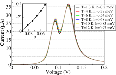
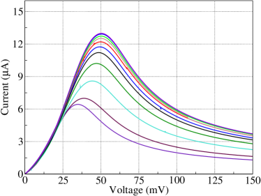
We now numerically simulate RTD – characteristics using Eq. (IV). We present the results in Fig. 6. In order to better distinguish the effects of the injector and the quantum well we vary both the temperature and the external magnetic field between curves. For each curve, a pair of and parameters are selected such that the giant Zeeman splitting in the quantum well is maintained at a constant value meV because all changes in magnetic field are compensated by a change in temperature as required by the modified Brillouin function [Eq. (1)]. For this reason, the splitting of the peaks are identical between adjacent curves. However, since each curve is acquired at a different , the Zeeman splitting in the injector , which is temperature independent, changes. As a result, the relative amplitude of the two peaks changes. At low temperatures, the applied field is small and the injected current is spin unpolarized. When is increased (and in order to keep constant), the injector becomes polarized and the majority spin current peak increases whereas at the same time the minority peak decreases. In the inset of Fig. 6 we show the expected polarization detected by the RTD, which exhibits a roughly linear dependence with , thus reinforcing the idea that the polarization can be measured via the change of the peak height.
We emphasize that the operating principle of this device lies in the giant Zeeman splitting in the well which allows us to separate the current into spin-up and spin-down flows and that the increase of only serves as a tool to generate spin polarizations in the injector. Obviously, any other polarization generating method would play a similar role.
V Conclusion
We have addressed nonlinear electron transport in magnetically doped II–VI resonant tunneling diodes. We have presented experimental data which shows that such devices can work as spin filters when the quantum well is magnetic. We have presented a simple theoretical model which accounts for the observed behavior and have proposed two devices in which spin effects are important.
The first device consists of a RTD with an emitter doped with Mn and a normal quantum well. Our model shows an enhancement and a voltage shift of the resonance current peak when the applied magnetic field increases. The results are consistent with a giant Zeeman splitting in the injector since the current saturates at a few Tesla and the temperature dependence follows the magnetization of a paramagnetic system. The Zeeman splitting induced redistribution of spin carriers in the injector leads to a modification of the conduction band structure of the device which is responsible for the changes in the transport properties. The results we obtain are reminiscent of Ref. [25], where the In content of a GaInAs emitter in a III-V RTD was varied. As a consequence, the band alignment changes and the peak current increases. In our case, the increase is due exclusively to the giant spin splitting in the injector, offering the unique possibility of producing high peak currents which arise from spin effects only. Thus, the current increase can be tuned with a magnetic field without changing the sample parameters.
The second device is a RTD where the central well is magnetically doped and the applied fields are high. Then, we have presented evidence that such a RTD can work as a detector of spin polarized currents. The Mn impurities in the well give rise to a giant Zeeman splitting which manifests itself in a splitting of the – characteristic. Further increase of the magnetic field leads to a change in the amplitude of the current peaks which is opposite for each spin index. Thus, this amplitude change is employed to estimate the injector’s spin polarization.
The theoretical model has considerable latitude for including complicated effects. It has been shown in Ref. [24] that electron-electron interactions (even at the mean-field level) can produce multistability of states with distinct spin polarizations for a given bias voltage. Depending on the carrier density, in multiple quantum well systems there may arise self-sustained oscillations of the spin polarization which occur without any time-dependent forcing [26]. In addition, a desirable property of any transport theory dealing with spin-polarized currents is that spin relaxation processes should be taken into account. These mechanisms can be rather slow in II–VI materials but their role can be discussed within a phenomenological model [24].
In closing, we believe that our discussion opens new research avenues toward an all-electrical generation, manipulation and detection of spin polarized currents in nanodevices.
Acknowledgment
We thank A. Slobodskyy, T. Slobodskyy and D.L. Supp for collaboration in the experiments and V. Hock for sample fabrication.
References
- [1] Semiconductor Spintronics and Quantum Computation, edited by D.D. Awschalom, D. Loss, and N. Samarth (Springer, 2002).
- [2] J.K. Furdyna and J. Kossut, Diluted Magnetic Semiconductors, vol. 25 of Semiconductor and Semimetals (Academic Press, New York, 1988); T. Dietl, Diluted Magnetic Semiconductors, vol. 3B of Handbook of Semiconductors (North-Holland, New York, 1994).
- [3] H. Ohno, “Making Nonmagnetic Semiconductors Ferromagnetic,” Science, vol. 281, pp. 951-956 (1998).
- [4] D.D. Awschalom and N. Samarth, “Spin dynamics and quantum transport in magnetic semiconductor quantum structures,” J. Magn. Magn. Mat., vol. 200, pp. 130-147 (1999).
- [5] R. Fiederling, M. Keimi, G. Reuscher, W. Ossau, G. Schmidt, A. Waag, and L.W. Molenkamp, “Injection and detection of a spin-polarized current in a light-emitting diode,” Nature (London), vol. 402, pp. 787-790 (1999).
- [6] Y. Ohno, D.K. Young, B. Beschoten, F. Matsukura, H. Ohno and D.D. Awschalom, “Electrical spin injection in a ferromagnetic semiconductor heterostructure,” Nature (London), vol. 402, pp. 790-792 (1999).
- [7] A. Slobodskyy, C. Gould, T. Slobodskyy, C.R. Becker, G. Schmidt, and L.W. Molenkamp, “Voltage-Controlled Spin Selection in a Magnetic Resonant Tunneling Diode,” Phys. Rev. Lett., vol. 90, pp. 246601 (2003).
- [8] T. Hayashi, M. Tanaka, and A. Asamitsu, “Tunneling magnetoresistance of a GaMnAs-based double barrier ferromagnetic tunnel junction,” J. Appl. Phys., vol. 87, pp. 4673-4675 (2000).
- [9] P. Bruno and J. Wunderlich, “Resonant tunneling spin valve: A novel magnetoelectronics device,” J. Appl. Phys., vol. 84, pp. 978-982 (1998).
- [10] N.N. Beletskii, G.P. Berman, and S.A. Borysenko, “Controlling the spin polarization of the electron current in a semimagnetic resonant-tunneling diode,” Phys. Rev. B, vol. 71, pp. 125325 (2005).
- [11] S. Ganguly, A.H. MacDonald, L.F. Register, and S. Banerjee, “Intrinsic Curie temperature bistability in ferromagnetic semiconductor resonant tunneling diodes,” Phys. Rev. B, vol. 73, pp. 033310 (2006).
- [12] C. Ertler and J. Fabian, “Resonant Tunneling Magneto Resistance in Coupled Quantum Wells,” cond-mat/0610617 (unpublished).
- [13] L.L. Chang, L. Esaki, and R. Tsu, “Resonant tunneling in semiconductor double barriers,” Appl. Phys. Lett., vol. 24, pp. 593-595 (1974).
- [14] E.R. Brown, T.C.L.G. Sollner, W.D. Goodhue, and C.D. Parker, “Millimeter-band oscillations based on resonant tunneling in a double-barrier diode at room temperature,” Appl. Phys. Lett., vol. 50, pp. 83-85 (1987).
- [15] E. Özbay, D.M. Bloom, D.H. Chow, and J.N. Schulman, “1.7-ps, microwave, integrated-circuit-compatible InAs/AlSb resonant tunneling diodes,” IEEE Electron Device Lett., vol. 65, pp. 400-402 (1993).
- [16] J.K. Furdyna, “Diluted magnetic semiconductors,” J. Appl. Phys., vol. 64, pp. R29-R64 (1988).
- [17] M.L. Leadbeater, E.S. Alves, L. Eaves, M. Henini, O.H. Hughes, A. Celesta, J.C Portal, G. Hill, and M.A. Pate, “Magnetic field studies of elastic scattering and optic-phonon emission in resonant-tunneling devices,” Phys. Rev. B,, vol. 39, pp. 3438-3441, (1989).
- [18] A.D. Martin, M.L.F. Lerch, P.E. Simmonds and L. Eaves, “Observation of intrinsic tristability in a resonant tunneling structure,” Appl. Phys. Lett., vol. 64, pp. 1248-1250 (1994).
- [19] S. Ben Amor, K.P. Martin, J.J.L. Rascol, R.J. Higgins, A. Torabi, H.M. Harris, and C.J. Summers, “Transverse magnetic field dependence of the current-voltage characteristics of double-barrier quantum well tunneling structures,” Appl. Phys. Lett., vol. 53, pp. 2540-2542 (1988)
- [20] S. Ben Amor, J.J. Rascol, K.P. Martin, R.J. Higgins, R.C. Doher, and H. Hier, “Transverse magnetic field studies in AlInAs/GaInAs quantum-well tunneling structures,” Phys. Rev. B, vol. 41, pp. 7860-7863(1990).
- [21] T. Dietl, H. Ohno, F. Matsukura, J. Cibert, and D. Ferrand, “Zener model description of ferromagnetism in zinc-blende magnetic semiconductors,” Science, vol. 287, pp. 1019-1022 (2000).
- [22] M. Büttiker, “Coherent and Sequential Tunneling in Series Barriers,” IBM J. Res. Develop., vol. 32, pp. 63-75 (1988).
- [23] Ya. Blanter and M. Büttiker, “Transition from Sub-Poissonian to Super-Poissonian Shot Noise in Resonant Quantum Wells,” Phys. Rev. B, vol. 59, pp. 10217-10226 (1999).
- [24] D. Sánchez, A.H. MacDonald, and G. Platero, “Field-domain spintronics in magnetic semiconductor multiple quantum wells,” Phys. Rev. B, vol. 65, pp. 035301 (2002).
- [25] Y.W. Choi and C.R. Wie, “Increased peak current in AlAs/GaAs resonant tunneling structures with GaInAs emitter spacer,” J. Appl. Phys., vol. 71, pp. 1853-1859 (1992).
- [26] M. Béjar, D. Sánchez, A.H. MacDonald, and G. Platero, “Spin-polarized current oscillations in diluted magnetic semiconductor multiple quantum wells,” Phys. Rev. B, vol. 67, pp. 045324 (2003).
| David Sánchez received his PhD degree in physics from the Autonomous University of Madrid in 2002 for theoretical work in nonlinear and spin-related properties of electronic nanodevices. He is currently an assistant researcher with the Department of Physics at the University of the Balearic Islands. His main interests include nonlinear mesoscopic transport, strongly correlated nanostructures and spintronics. |
| Charles Gould completed his PhD in mesoscopic transport physics in a co-operative program between Sherbrooke University and the National Research Council of Canada (CNRC) in 2000. Since September 2000, he has been working as a post-doc/scientific assistant in the group of Prof. Molenkamp, doing transport work in semiconductor spintronics with a large focus on (Ga,Mn)As-based devices. |
| Georg Schmidt did his PhD in Aachen working on Si/SiGe deposition and nanolithography. In 1996 he joined the group of Prof. Molenkamp in Aachen and started the activities on spintronics and nanolithography. Since 1999 he is in Wuerzburg at the Chair of Prof. Molenkamp, where he is the head of the workgroup for spintronics and nanolithography. His main focus is on spin transport and ultra high resolution lithography. |
| Laurens Molenkamp’s background includes the optical and quantum transport studies in semiconductor nanostructures and spintronics. He was appointed Professor of Experimental Physics (C3) at the RWTH in Aachen, Germany, in 1994. He moved to Wuerzburg University in April 1999 as the Chair of Experimental Physics (EP3), where he continues research in spintronics and spin-related phenomena. |