Spin dependent resonant tunneling through 6 micron diameter double barrier resonant tunneling diode
Abstract
A vertical resonant tunneling diode (RTD) based on the paramagnetic Zn1-x-yMnyCdxSe system has been fabricated with a pillar diameter down to 6 m. The diode exhibits high quality resonant tunneling characteristics through the electron sub-band of the quantum well at a temperature of 4.2 K, where a clear phonon replica was observable in addition to the primary peak. Both peaks show a giant Zeeman splitting in an applied magnetic field. Employing a self-consistent real-time Green’s function method, the current-voltage characteristic was simulated, showing good agreement with the measured result.
The II-VI paramagnetic semiconductor system has emerged as one of the most promising for spintronic devices due to the presence of the unique giant Zeeman splitting.1 ; 2 For example, Slobodskyy and Maximov et al. have reported voltage-controlled spin selection in ZnMnSe magnetic RTDs and micro-patterned RTDs.3 ; 4 In principle, the II-VI system should allow easy tunability via gating, once a solution for the dielectric leakage problem is found, as was done in non-magnetic III-V systems.5 Up to now, ZnMnSe is the typical II-Mn-VI system of choice since ZnSe is lattice matched to GaAs substrate with only 0.27% in-plane mismatch.3 ; 4 On the other hand, the partial substitution of Zn with Cd to form Zn1-xCdxSe alloys allows the band gap to be tuned, with an energy gap varying from 1.75 eV for CdSe to 2.71 eV for ZnSe.2 The Zn1-xCdxSe system is thus more versatile and potentially important for combining optical and electrical devices on the same chip. However, this comes at the expense of a much larger lattice mismatch leading to a high density of defects.6 The room temperature cubic lattice constants for ZnSe, GaAs and CdSe are 5.67, 5.65 and 6.05 Å respectively.2 Therefore, it is challenging to integrate paramagnetic Zn1-x-yMnyCdxSe into the device for spintronics application.

In this letter, we report the successful fabrication of a 6 m diameter sized magnetic RTD in the Zn1-x-yMnyCdxSe system. Because of the small size we were able to avoid the problem of a lack of homogeneity in the crystal often encountered in II-VI growth. Our RTD, fabricated at a randomly chosen local region, demonstrates excellent resonant tunneling characteristics: high peak-to-valley current ratio in the negative differential conductance (NDC), clear Zeeman splitting of the resonance peaks in the tunneling current in the presence of a magnetic field, and a distinct phonon replica. We present a complete device allowing voltage-controlled spin selection with a self-aligned (but leaky) gate in place. We are able to successfully explain the NDC characteristics by employing a numerical simulation based on a self-consistent Green’s function method.
Our double barrier tunneling (DBT) crystal structure for the RTD device was grown by molecular beam epitaxy using a GaAs (100) substrate, as depicted in Figure 1. The DBT consists of a 600 nm n+ ZnSe:Cl layer (Cl doping: 31018 cm-3) for the bottom electrical contact, a 3.0 nm undoped ZnSe spacer, a 3.0 nm Zn0.62Mn0.08Be0.3Se barrier, a 6.0 nm Zn0.83Mn0.1Cd0.07Se quantum well, another 5.0 nm Zn0.62Mn0.08Be0.3Se barrier and 3.0 nm undoped ZnSe spacer, and a 65 nm n+ Zn0.92Cd0.08Se:Cl (2.51018 cm-3) cap layer for a top contact, which is designed to be thin, in anticipation of future devices with local magnetic fields close to the quantum well produced by nanomagnets or small superconductors at the surface.7 The DBT was patterned into a 6 m pillar by a complex, five e-beam lithography step process. It is surrounded with a self-aligned Ti/Au gate, deposited on a SiOx insulator as shown in the insert to Figure 1. We note that the electrical contacts for the RTD are made ex-situ, which is difficult for II-VI systems.8 The contacts were produced by first evaporating a 200 nm thick indium disk on top of the tunneling pillar, followed by annealing at a temperature of 200 ∘C for one minute. Although in-situ deposition of the top metallic contact is often preferable,3 ; 4 by precisely controlling the annealing process, we are able to consistently diffuse indium into the top Zn1-xCdxSe:Cl layer over a contact area of several microns to achieve good tunneling characteristics. In addition, our device has a 2 m wide ridge connecting the tunneling pillar to a large wire bonding pad. This extra connecting ridge is necessary as a precursor to devices with local magnetic fields, where the magnetic structures must be placed on the pillar top surface.7
The transport characterization under magnet field was carried out by inserting the sample into an Oxford 4He bath cryostat mounted with a 6 T superconducting magnet. The magnetic field is applied parallel to the current flow through the RTD, and positive bias corresponds to the top, capping layer biased positively. All the data we present were measured without gating. At present, our gate dielectric SiOx (200 nm) is leaky, with only a low leakage window between 0.8 to 0.5 V, too small to affect the tunneling characteristics.
The zero magnetic field current-voltage (I-V) and dI/dV-V characteristics taken at T=4.2 K are shown in Figure 2(a). A comparison of the I-V curves measured before and after the precision annealing of the top indium contact indicates good contact formation and excellent resonant tunneling behavior after annealing. Two distinct peaks, P1 and P2, were observed in the I-V curve; P1 and P2 have peak-to-valley ratio of 3:1 and 2:1, respectively. Both show distinct negative-differential-conductance, a key characteristic of resonant tunneling through a DBT structure. P1 was located at around 0.54 V and the separation between P1 and P2 is about 105 mV. We attribute P1 to the tunneling through the second electron sub-band in the quantum well (see following analysis). The separation between P1 and P2 enabled us to attribute P2 to the LO-phonon assisted in-barrier tunneling.3 The sharpness of this replica further indicates the high quality of RTD. We ruled out tunneling through the bonding pad as the source of the resonance peaks. Firstly, the thin ridge turned out to be insulating because the etched side walls contain traps that prevent the doping charge in the top n+ Zn1-xCdxSe:Cl layer (65 nm thick) from conducting. Secondly, cutting off the 6 m pillar by cutting the ridge removed the two peaks P1 and P2.
In Figure 2(b) we show the I-V characteristics under different magnetic fields. P1 and P2 each split into two peaks due to the giant Zeeman splitting. This splitting is repeatable and reversible for both field directions. At the maximum field (6 T) both have splitting magnitude 60 mV. This similar magnetic behavior further lends support to the identification of P2 as the LO-phonon replica of P1.
A self-consistent real-time Green’s function method was employed to simulate the primary peak (P1) resonant tunneling behavior.9 We use 22% valence band offset (VBO) of ZnBeSe over ZnMnSe10 to estimate the VBO of the barrier and well layers, which gives around 670 meV conduction band potential in the well. The simulated I-V curve at 4.2 K using the nominal quantum well width of 6 nm indicates that the lowest two tunneling peaks should occur at lower bias voltages than P1 (dotted curve in Figure 3(a)). Tunneling peak position is mainly affected by the Fermi level (carrier concentration) and the well width. Since the carrier concentration in highly doped ZnSe:Cl is temperature independent,11 the difference between simulation and experiment is likely caused by fluctuations in the width. Indeed, the resonant peak position was found to vary in different parts of the crystal. With the well width as the only adjustable parameter, we fitted to a modified value of 5 nm. All other parameters such as electron effective mass , dielectric constant and the energy gap were found experimentally or in the literature.12 The simulated I-V characteristic based on the 5 nm well width has the second peak position in good agreement with the experimental location of P1 (dashed curve in Figure 3(a)). Therefore we attribute P1 to tunneling through second electron sub-band. Figure 3(a) insert shows the resultant simulated band structure, local state density and transmission at zero source-drain voltage. The reason tunneling through the first sub-band was not observed may be explained by the extremely low transmission on a high current background.

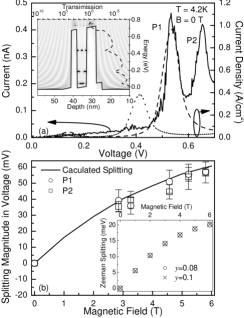
The magnetic field dependence of the Zeeman splitting in the conduction band in a II-Mn-VI semiconductor can be expressed as:2 ; 13 ; here, x is the Mn concentration; eV is the -d exchange constant; , , and are the g-factor, manganese spin, Bohr magneton, and Boltzmann constant, respectively. represents the Brillouin function of spin . The value of (0.95) and K (2.70 K) for Mn composition of (0.1) are achieved by interpolating values taken from the literature.14 Assuming conduction band splitting is only significant in the barriers and well, a two-current model to simulate each spin channel independently is employed while neglecting the spin-coupling and scattering disorder.15 The simulated splitting of the tunneling current peak through the second electron level versus magnetic field is plotted as solid line and is compared with the splitting of P1 (circles) and P2 (squares) in Figure 3(b). The simulated result is in good agreement with experimental data.
For a RTD with negligible series resistance, the energy difference in the well can be related to the voltage difference by lever arm factor : . originates from the fact that only part of the applied voltage is dropped on the emitter. Our RTD has a thinner emitter barrier which further lowers the voltage drop compared to the symmetric case, resulting in larger splitting. Comparing the 20 meV Zeeman splitting of the electron level at 6 T field with the 60 mV splitting observed in the resonant tunneling peaks, we find . Thus, we deduced a phonon energy of 35 meV from the P1 and P2 separation of 105 meV, close to the known LO phonon energy of 31 meV in ZnBeSe alloy.16
In conclusion, we report the successful fabrication of micron sized magnetic RTD based on the paramagnetic ZnMnCdSe system with a self-aligned gate. Clear NDC, Zeeman splitting of resonant tunneling peaks, as well as a phonon replica were demonstrated. We demonstrate good control on ex-situ Ohmic indium contacts, which is usually difficult to achieve in II-VI system. Our results suggest that further work to tune the system electrically may be possible following improvements in gate performance.
Acknowledgement: This work was supported in part by NSF DMR-02105191.
References
- (1) I. Žutić, J. Fabian, and S. Das Sarma, Rev. Mod. Phys. 76, 323 (2004).
- (2) J. K. Furdyna, J. Appl. Phys. 64, R29 (1988).
- (3) A. Slobodskyy, C. Gould, T. Slobodskyy, C. R. Becker, G. Schmidt, and L. W. Molenkamp, Phys. Rev. Lett. 90, 246601 (2003).
- (4) S. Maximov, T. Slobodskyy, A. Gröger, F. Lehmann, P. Grabs, L. Hansen, C. R. Becker, C. Gould, G. Schmidt, and L. W. Molenkamp, Semicond. Sci. Technol. 19, 946 (2004).
- (5) S. Tarucha, D. G. Austing, T. Honda, R. J. van der Hage, and L. P. Kouwenhoven, Phys. Rev. Lett. 77, 3613 (1996).
- (6) N. Samarth, H. Luo, J. K. Furdyna, R. G. Alonso, Y. R. Lee, A. K. Ramdas, S. B. Qadri, and N. Otsuka, Appl. Phys. Lett. 56, 1163 (1990).
- (7) M. Berciu, T. G. Rappoport, and B. Jankó, Nature 435, 71 (2005); M. Berciu and B. Jankó, Phys. Rev. Lett. 90, 246804 (2003).
- (8) L. Hernández, O. de Melo, M. Meléndez-Lira, Z. Rivera-Alvarez, and I. Hernández-Calderón, J. Vac. Sci Technol. A 14, 2269 (1996).
- (9) K. M. Indlekofer and J. Malindretos, WinGreen Simulation Package, http://www.fz-juelich.de/isg/mbe/wingreen.html.
- (10) K. Godo, H. Makino, M. W. Cho, J. H. Chang, S. K. Hong, T. Yao, M. Y. Shen, and T. Goto, J. Appl. Phys. 91, 5811 (2002).
- (11) C. Boney, Z. Yu, W. H. Rowland, Jr., W. C. Hughes, J. W. Cook, Jr., J. F. Schetzina, G. Cantwell, and W. C. Harsch, J. Vac. Sci. Technol. B 14, 2259 (1996).
- (12) I. Strzalkowski, S. Joshi, and C. R. Crowell. Appl. Phys. Lett. 28, 350 (1976); B. G. Streetman, Solid State Electronic Devices, Prentice Hall (1990); G. P. Srivastava, H. M. Tütüncü, and N. Günhan, Phys. Rev. B 70, 085206 (2004); D. T. F. Marple, J. Appl. Phys. 35, 1879 (1964); C. Y. Wu, Y. K. Li, and C. C. Tu, IEEE Conference on Nanotechonlogy 2, 763 (2003); D. J. Stukel, Phys. Rev. B 2, 1852 (1970).
- (13) J. A. Gaj, R. Planel, and G. Fishman, Solid State Commun. 29, 435 (1979).
- (14) W. Y. Yu, A. Twardowski, L. P. Fu, A. Petrou, and B. T. Jonker, Phys. Rev. B 51, 9722 (1995); A. Twardowski, M. von Ortenberg, M. Demianiuk, and R. Pauthenet, Solid State Commun. 51, 849 (1984).
- (15) M. K. Li, N. M. Kim, S. J. Lee, H. C. Jeon, and T. W. Kang, Appl. Phys. Lett. 88, 162102 (2006); P. Havu, N. Tuomisto, R. Väänänen, M. J. Puska, and R. M. Nieminen, Phys. Rev. B 71, 235301 (2005).
- (16) O. Pagès, M. Ajjoun, J. P. Laurenti, D. Bormann, C. Chauvet, E. Tournié, and J. P. Faurie, Appl. Phys. Lett. 77, 519 (2000).