Rayleigh Imaging of Graphene and Graphene Layers
Abstract
We investigate graphene and graphene layers on different substrates by monochromatic and white-light confocal Rayleigh scattering microscopy. The image contrast depends sensitively on the dielectric properties of the sample as well as the substrate geometry and can be described quantitatively using the complex refractive index of bulk graphite. For few layers (6) the monochromatic contrast increases linearly with thickness: the samples behave as a superposition of single sheets which act as independent two dimensional electron gases. Thus, Rayleigh imaging is a general, simple and quick tool to identify graphene layers, that is readily combined with Raman scattering, which provides structural identification.
Graphene is the prototype two dimensional carbon system geimrev . Its electron transport is described by the (relativistic-like) Dirac equation and this allows access to the rich and subtle physics of quantum electrodynamics in a relatively simple condensed matter experiment Novoselov2005proc ; Novoselov2005nature ; Zhang2005nature ; Novoselov2004 ; Novoselov2006 . The scalability of graphene devices to true nanometer dimensionskimribbon ; Lemme ; avouris makes it a promising candidate for future electronics, because of its ballistic transport at room temperature combined with chemical and mechanical stability. Remarkable properties extend to bi-layer and few-layers Novoselov2004 ; Novoselov2006 ; Zhang2005apl ; Berger2004 ; Scott2005 . More fundamentally, the various forms of graphite, nanotubes, buckyballs can all be viewed as derivatives of graphene.
Graphene samples can be obtained from micro-mechanical cleavage of graphite Novoselov2005proc . Alternative procedures include chemical exfoliation of graphite Viculis03 ; Viculis05 ; Niyogi06 ; Stankovich06 ; Stankovich06JMC or epitaxial growth by thermal decomposition of SiC Berger2004 ; Forbeaux99 ; Ohta06 ; Rolling06 . The latter has the potential of producing large-area lithography compatible films, but is substrate limited. It is hoped that in the near future efficient large area, substrate independent, growth methods will be developed, as it is now the case for nanotubes.
Despite the wide use of the micro-mechanical cleavage, the identification and counting of graphene layers is still a major hurdle. Monolayers are a great minority amongst accompanying thicker flakes geimrev . They cannot be seen in an optical microscope on most substrates. Currently, optically visible graphene layers are obtained by placing them on the top of oxidized Si substrates with typically 300 nm SiO2. Atomic Force Microscopy (AFM) is viable but has a very low throughput. Moreover, the different interaction forces between the AFM probe, graphene and the SiO2 substrate, lead to an apparent thickness of 0.5-1 nm even for a single layer Novoselov2005proc ; Novoselov2004 , much bigger of what expected from the interlayer graphite spacing. Thus, in practice, it is only possible to distinguish between one and two layers by AFM if graphene films contain folds or wrinkles Novoselov2005proc ; Novoselov2004 . High resolution transmission electron microscopy is the most direct identification tool meyer ; acf , however, it is destructive and very time consuming, being viable only for fundamental studies meyer .
Optical detection relying on light scattering is especially attractive because it can be fast, sensitive and not-destructive. Light interaction with matter can be elastic or inelastic, and this corresponds to Rayleigh and Raman scattering, respectively. Raman scattering has recently emerged as a viable, non-destructive technique for the identification of graphene and its doping acf ; Pisana . However, Raman scattered photons are a minority compared to those elastically scattered. Here we show that the elastically scattered photons provide another very efficient and quick means to identify single and multi-layer samples and a direct probe of their dielectric constant.
Rayleigh scattering was previously used to monitor size, shape, concentration and optical properties of nano-particles, carbon nanotubes and viruses lukas ; vahid ; antonio ; tony ; tony2 . Rayleigh scattering experiments can be performed using two different strategies. In one, the background signal is minimized by making free-standing samples, as done in the case of carbon nanotubes tony ; tony2 , or by dark-field configurations dark . Alternatively, the background intensity is utilized as a reference beam, while the sample signal is detected interferometrically lukas ; vahid ; antonio ; kim ; calatroni . Here, we combine the second approach with the interferometric modulation of the contributing fields and we show that the presence of a background is essential to enhance the detection of graphene over a certain wavelength range.
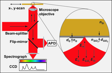
Graphene samples are produced by micro-mechanical cleavage of bulk graphite and deposited on a Si substrate covered with 300 nm SiO2 (IDB Technologies LTD). The sample thickness is independently confirmed by a combination of AFM and Raman spectroscopy. AFM is performed in tapping mode under ambient conditions. Raman spectra are measured at 514 nm using a Renishaw micro-Raman 1000 spectrometer. Rayleigh scattering is performed with an inverted confocal microscope, Fig.1. Either a He-Ne laser (633 nm) or a collimated white-light beam are used as excitation source. Coherent white-light pulses are generated by pumping a photonic crystal fibre with the output of a Ti:Sa oscillator operating at 760 nm. The beam is reflected by a beam splitter and focused by a microscope objective with high numerical aperture (NA= 0.95). However,the objective lens is not totally filled, which results in an effective NA0.7 thereby increasing the image contrast as discussed at the end of this paper. The scattered light from the sample is collected in backscattering geometry, transmitted by a beam splitter and detected by a photon-counting avalanche photodiode (APD), Fig.1. Alternatively, the reflected light is filtered using a notch filter to remove the laser excitation and sent to a spectrometer. This allows simultaneous Rayleigh and Raman measurements, Fig.1,2a. Confocal Rayleigh images are obtained by raster scanning the sample with a piezoelectric scan stage. The acquisition time per pixel varies from few ms in the case of Rayleigh scattering to few minutes for Raman scattering. This empirically indicates that Rayleigh measurements are almost 5 orders of magnitude quicker than Raman measurements. The spatial resolution is 800 nm.
Fig.2(b) shows an AFM image of monolayer graphene. The AFM cross section gives an apparent height of 0.6 nm. Raman spectroscopy confirms that the sample is a single layer (Fig.2(a)) acf . Fig.2(b) is the corresponding confocal Rayleigh image obtained with monochromatic laser light (633 nm).
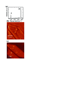
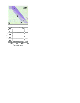
Fig.3(a) shows an optical micrograph of a sample composed of a varying number of layers. Once the single layer is identified by Raman scattering, we get the total number of layers from the measured AFM height, considering the interlayer spacing of 0.33 nm: z [nm]= 0.27 + 0.33 N. This confirms that the sample is composed of 1, 2, 3 and 6 layers, as for Fig.3 (a). These layers have a slightly different color in the optical microscope (Fig.3 (a)). It appears that the darker color corresponds to the thicker sample. Note, however, that the color of much thicker layers (more than 10 layers) does not follow this trend and can change from blue, to yellow, to grey. The number of layers is further confirmed by the evolution of the 514 nm Raman spectra acf ,Fig. 3 (b). Fig.4(a) shows a confocal Rayleigh map for 633nm excitation. The signal intensity of in Fig.4 appears to increase with N.
We now discuss the physical origin of the image contrast (). This is defined as the difference between substrate and sample intensity, normalized to the substrate intensity. The single layer contrast at 633 nm is . The contrast is positive, i.e. the detected intensity from graphene is smaller than that of the substrate. The Rayleigh images in Fig.2 (c) and Fig.4 (a) are reversed for convenience, in order to compare them with AFM.
We explain the sign and scaling of the contrast for increasing N in terms of interference from multiple reflections. The inset in Fig.1 shows a schematic of the interaction between the light and graphene on Si+SiO2. When the light impinges on a multi-layer, multiple reflections take place wolf . Thus, the detected signal (I) results from the superposition of the reflected field from the air-graphene (), graphene-SiO2 (), and SiO2-Si interfaces (). The back-ground signal () results from the superposition of the reflected field from the air-SiO2 interface and the Si substrate.
Before giving a complete quantitative model, it is useful to consider a simplified picture that captures the basic physics and illustrates why a single atomic layer can be visualized optically. The field at the detector is dominated by two contributions: the reflection by the graphene layer, and the reflection from the Si after transmission through graphene and after passing through the SiO2 layer twice. Thus, the intensity at the detector can be approximated as:
| (1) |
where is the total phase difference. This includes the phase change due to the optical path length of the oxide, , and that due to the reflection at each boundary, and :
| (2) |
where is the refractive index of the oxide and is the wavelength of the light in vacuum. Assuming the field reflected from graphene to be very small, , the image contrast results from interference with the strong field reflected by the silicon:
| (3) |
The sign of depends on the sign of , which is given by Eq. 2. The reflectance, R, is the ratio between the reflected power to the incident power wolf . Assuming the Si reflectance as one, Eq. 3 can be written as:
| (4) |
where is the reflectance of graphene. This is in turn related to the reflection coefficient wolf :
| (5) |
Eq. 4 shows that the main role of the SiO2 is to act as a spacer: the contrast is defined by the phase variation of the light reflected by the Si jcp . Thus, the contrast for a given wavelength can be tailored by adjusting the spacer thickness or its refractive index.
In order to investigate the wavelength dependence of the image contrast, we perform Rayleigh spectroscopy with a white-light source. A grating is used to analyze the detected light. Fig.4 (b) shows that for N=1 the contrast is maximum at 570 nm. The contrast at 633 nm is 0.08, in agreement with the monochromatic Rayleigh scattering experiment. The contrast is zero at 750 nm and it is small and negative for 750 nm. From Eqs. 2 and 4 and assuming , the phase of graphene is as expected for an ultra-thin film wolf . The contrast decreases in the near IR (for = 300 nm) since the wavelength becomes larger than twice the optical path length provided by the SiO2-spacer. Fig. 4 (b) shows that while the contrast increases for increasing N, the phase remains constant.
We now present a more accurate model, with no assumptions, which describes the light modulation by multiple reflections based on the recurrent matrix method for reflection and transmission of multilayered films hecht . We calculate the total electric and magnetic fields in the various layers, applying the boundary conditions at every interface. The fields at two adjacent boundaries are described by a characteristic matrix. This depends on the complex refractive index and the thickness of the film and the angle of the incident light hecht . By computing the characteristic matrix of every layer and taking into account the numerical aperture of the objective and the filling factor, it is possible to find the reflection coefficient for an arbitrary configuration of spacer (2) and substrate (3) and for any number of graphene layers (G). Assuming two counter-propagating waves, the standard boundary conditions for the reflection coefficient of a normally incident wave is:
| (6) |
where
| (7) |
| (8) |
with and . For incidence at an angle , with s-polarization (transverse electric field), the same formula applies with the substitution , while for p-polarization every ratio changes . The phases change in both s and p polarizations to and . The angle for every layer is obtained from Snell’s law: . In case any of the layers is absorbing (as in graphene and Si), we need use an effective index which depends on the incident angle from vacuum wolf ; ciddor . In this case the corresponding refraction angle is .
The matrix method requires as input the complex refractive index of the sample. The frequency dependent Si and SiO2 indexes are taken from Ref. palik . For graphene, few layers graphene and graphite, this is anisotropic, depending on the polarization of the incident light. For electric field perpendicular to the graphene c-axis (in-plane) we need , while for electric field parallel to the c-axis we need . To get these, we use the experimental refractive index taken from the electron energy loss spectroscopy measurements on graphite of Ref. japgraphite . For s-polarized light (electric field restricted in the plane) the refractive index to be used is simply . For p-polarization, both in-plane and out-of-plane field components exists. Thus we have an angle dependent refractive index , where the refracted angle has to be calculated self-consistently with Snell’s law. In order to account for the numerical aperture in the experiment, we need to integrate the response of all possible incident angles and polarizations with a weight distribution accounting for the Gaussian beam profile used in the experiment , where .
Fig.4(b) shows the calculated contrast for N between 1 and 6 (lines). This is in excellent agreement with the experiments: i) the contrast scales with number of layers; ii) it is maximum at 570 nm; iii) no phase shift is observed in this N range. Thus, for N between 1 and 6, . The contrast of graphene at 570 nm is 0.1. From Eqs. 4 and 5 we get (= 570 nm)= 0.05. Thus, (= 570 nm)= 0.003.
It quite remarkable that, without any adjustable parameter, graphene’s response can be successfully modeled using graphite’s dielectric constant. This implies that the optical properties of graphite do not depend on the thickness, i.e. graphene and graphite have the same optical constants. The electrons within each graphene layer form a two dimensional gas, with little perturbation from the adjacent layers, thus making multi-layer graphene optically equivalent to a superposition of almost non-interacting graphene layers. This is intuitive for s-polarization. However, quite notably this still holds when the out-of-plane direction (p-polarization) is considered. This is because, compared to the in-plane case, graphite’s response is much smaller, and in addition it gets smeared out by the NA integration. Thus, the maximum contrast (= 570 nm) of a N-layer is: . Fig. 6(a) shows that this approximation fails for large N. When valid, the relation between topography and contrast is given by: z[nm]= 0.27 + 3.3.
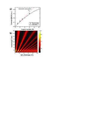
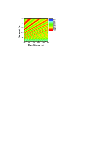
Fig.5(b) plots the contrast as a function of wavelength and SiO2 thickness for a single layer. The maximum contrast occurs at the minima of the background reflectivity. This is expected because this is the most sensitive point in terms of phase matching, and small changes become most visible. Thus, the optimal configuration requires the SiO2 to be tuned as an anti-reflection (AR) coating, i.e. with its optical length a quarter wavelength. The yellow dotted lines trace the quarter-wave condition , and indeed they closely follow the calculated contrast maxima. A second point of interest are the bright spots around 275 nm. These are due to the absorption peak at the transition of graphite japgraphite . For this excitation, the graphene mono-layer not only becomes much more visible, but the contrast change also directly reveals the frequency dependence of the graphene’s refractive index. Thus, as for nanotubes tony ; tony2 , white light Rayleigh scattering is a direct probe of the dielectric function.
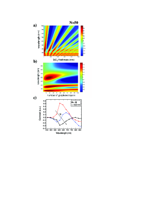
For thicker samples () the phase change due to the optical path in graphite cannot be neglected. Fig.6(a) shows the calculated contrast for a 50 layer sample as a function of SiO2 thickness, while Fig.6(b) plots the contrast for a fixed 300nm SiO2 thickness, but for a variable number of layers. At 633 nm, as N increases, the response first saturates, then decreases and red-shifts, finally becoming negative, as found experimentally (Fig. 6 (c)). It is also interesting to note that for small N the variation along the vertical (wavelength) axis is largely between zero and positive (i.e. reflectivity reduction only), while for large number of layers, the variation is from positive to negative (i.e. both reflectivity reduction and enhancement). This points to two different mechanisms. For small N, the effect of the graphene layers is just to change the reflectivity of the air/SiO2 interface, while they offer no significant optical depth. For large N, on the other hand, the reflectivity of the air/graphene interface saturates while the effect of the increasing optical path within the now thick graphite layer becomes significant. This change is not a monotonic function of N. While these two effects are different, they both contribute to a shift of the reflectivity resonance condition, and thus explain the increasing opaqueness of thicker graphene layers, when measured for a fixed excitation energy.
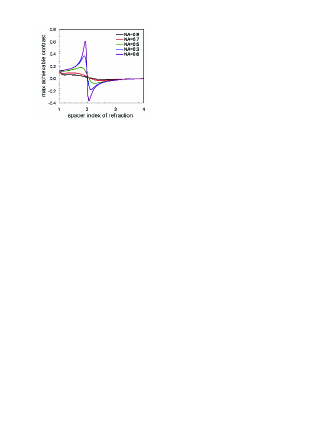
It is also interesting to consider the contrast as a function of NA. The calculations show that measurements at a reduced NA would give a stronger contrast, as one could intuitively expect. However, there is a nontrivial implication when varying NA, if one tries to maximize the contrast by using the anti-reflection coating rule for the spacer. The ideal AR coating over a substrate of index must have an index and quarter wave thickness . Since at 600 nm, it is natural to think that a spacer of n=2 (e.g. Si3N4) would be ideal. To explore this, Fig. 7 plots the contrast for different NAs as a function of at 600nm and for spacer thickness , which serves to maintain the AR condition and thus the maximum response.
Contrary to expectations, the contrast maximizes for different spacer indexes depending on NA. For normal incidence, it is maximum at 1.93 with a huge contrast of 0.6 for a single layer, Fig. 7. It also has a strong variation thereafter, and becomes negative. As NA further increases, the peak moves to a smaller index (around 1.5 for NA=0.7), becomes relatively flat, and eventually goes to . Thus, for large NA, it makes little difference what the spacer index is, as long as the quarter-wave condition is satisfied. Indeed, for the ideal AR condition the background reflectivity goes to zero and thus the contrast becomes large, however this condition strongly depends on the incidence angle and is thus easily destroyed at large NAs. For all possible spacer refractive indexes, a reduction in NA results into an increased contrast, however, the magnitude of this increase varies: at n=1.5 going from 0.7 to 0.0 NA changes the contrast by a factor 2, while at n=1.9 one can gain a factor of 6, Fig. 7. For maximum visibility, a spacer of thickness 225nm with NA=0.0 would be ideal. However,if high resolution is needed, as for nano-ribbons or, in general, to analyze edges and defects, a compromise between resolution and image contrast is necessary.
A second point to note is that for all NAs the contrast converges to the same value for n=1, i.e. for a suspended graphene layer over the substrate. Indeed, optically visible suspended layers were recently reported (see Fig.1 of Ref. bunch ). Maximum visibility is achieved if the quarter-wave condition is satisfied, as indeed in Ref. bunch , where the 300 nm SiO2 spacer is etched to create an air gap between graphene and the Si substrate. Interestingly, in this case any measurement with any NA will yield the same contrast. The same considerations are relevant for the case of a thin free-standing spacer (no substrate). By tuning at the low reflection point (now at half-wavelength) and with an NA=0.0 one could get fair contrasts. However, as soon as NA increases, the resonance condition is destroyed and the contrast becomes much smaller than for the SiO2/Si system.
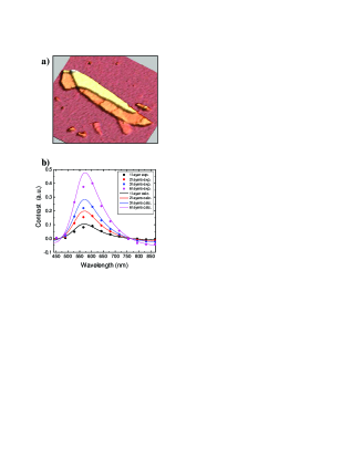
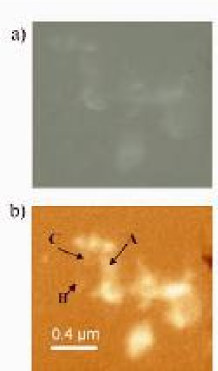
The matrix method can be extended to every film configuration. To prove this, we measure graphene layers on glass. For N=1, the calculated contrast at 633 nm is expected to be-0.01. Note the different sign compared with the Si/SiO2 substrate. This is due to the different optical properties of glass and Si. Fig.8(a) shows an optical micrograph of a multi-layer and Fig.8(b) the corresponding Rayleigh image at 633 nm. Raman spectroscopy shows that the sample is composed of layers of different thickness: A (7-10 layers), B (3-6 layers), C (1-2 layers). Although the contrast is lower compared to Si/SiO2, Rayleigh spectroscopy allows a better contrast and resolution compared with the optical microscope, where 10 layers are already difficult to detect and single layers are practically invisible. Note that the use of UV light could enhance the contrast to -0.04 at 300 nm excitation (Fig. 9 (b)).
In conclusion, we used white light illumination combined with interferometric detection to study the contrast between graphene and Si/SiO2 substrates. We modeled the light modulation by multiple reflections, showing that: i) the contrast can be tailored by adjusting the SiO2 thickness. Without oxide, no modulation is possible; ii) the light modulation strongly depends on the graphite thickness. For few layers () the samples behave as a superposition of single sheets. For thicker samples, both amplitude and phase change with thickness. Thus, Rayleigh spectroscopy provides a simple and quick way to map graphene layers on a substrate. It can also be combined with Raman scattering, which is capable of structural identification.
Acknowledgements.
The authors acknowledge A.K. Geim for useful discussions. CC acknowledges S. Reich for useful discussions. CC acknowledges support from the Oppenheimer Fund. ACF from the Royal Society and Leverhulme Trust. HH from the School of Graduate Studies G. Galilei (University of Pisa). AH from the German Excellence Initiative via the Nanosystems Initiative Munich (NIM).
References
- (1) Geim, A.K.; Novoselov, K.S. Nature Materials, 2007,6, 183.
- (2) Novoselov, K.S.; Jiang, D.; Schedin, F.; Booth, T.J.; Khotkevich, V.V.; Morozov, S. V. Proc. Natl. Acad. Sci.USA 2005, 102, 10451.
- (3) Novoselov, K.S.; Geim, A.K.; Morozov,S.V.; Jiang, D.; Katsnelson, M.I.; Grigorieva, I. V.; Dubonos, S.V.; Firsov, A.A. Nature 2005, 438, 197.
- (4) Zhang, Y.; Tan, Y.W.; Stormer, H.L.; Kim, P.; Nature 2005, 438, 201.
- (5) Novoselov, K.S.; Geim, A.K.; Morozov, S.V.; Jiang,D.; Zhang, Y.; Dubonos,S.V.; Grigorieva, I.V.; Firsov,A.A. Science 2004, 306, 666.
- (6) Novoselov, K.S.; McCann, E.; Morozov, S.V.;Falko, V.I.; Katsnelson, M.I.; Zeitler, U.;Jiang,D.; Schedin, F.; Geim, A.K., Nature Physics 2006,2, 177.
- (7) Han,M.Y.; Ozyilmaz, B.; Zhang, Y.; Kim,P. cond-mat/0702511 (2007)
- (8) Lemme, M.C.; Echtermeyer, T.J.; Baus, M.; Kurz, H. IEEE Electr. Device Lett. 2007,28, 282.
- (9) Chen, Z.; Lin, Y.M.; Rooks, M.J.;Avouris,P. cond-mat/0701599 (2007)
- (10) Zhang, Y.;Small, P.J.; Pontius, W.V.; Kim, P. Appl. Phys. Lett. 2005, 86, 073104.
- (11) Berger, C.;Song,Z.; Li,T.; Li,X.; Ogbazghi, Y.; Feng, R.; Dai,Z.; Marchenkov,A.N.; Conrad, E.H.; First, P.N. J. Phys. Chem. B 2004, 108, 19912.
- (12) Scott Bunch, J; Yaish, Y.; Brink,M.; Bolotin,K.; McEuen,P.L. Nano Lett. 2005, 5, 287.
- (13) Viculis, L.M.; Mack,J.J.;Kaner, R.B. Science 2003, 299, 5611.
- (14) Viculis, L.M.; Mack, J.J.; Mayer, O.M.; Hahn, H.T.; Kaner, R.B. J. Mater. Chem. 2005, 15, 9.
- (15) Niyogi,S.; Bekyarova, E.; Itkis, M.E.; McWilliams, J.L.; Hammon, M.A.; Haddon, R.C.; J. Am. Chem. Soc. 2006,128, 1720.
- (16) Stankovich,S.; Dikin,D.A.; Dommett, G.H.B.; Kohlhass,K.M.; Zimmey, E.J.; Stach,E.A.; Piner, R.D.; Nguyen, S.B.T.; Ruoff, R.S. Nature 2006, 442, 282.
- (17) Stankovich,S.; Piner,R.D.; Chen, X.; Wu,N.; Nguyen,T.; Ruoff, R.S.; J. Mater. Chem. 2006,16, 155.
- (18) Forbeaux, I.; Themlin, J.M.; Debever, J.M.; Surf. Science 1999,442, 9.
- (19) Ohta,T.; Bostwick,A.; Seyller, T.; Horn,K.; Rotenberg,E. Science 2006,313 951.
- (20) Rolling,E.; Gweon,G.H.; Zhou,S.Y.; Mun, B.S.; McChesney,J.L.; Hussain,B.S.; Fedorov,A.; First,P.N.; de Heer,W.A.; Lanzara,A. J. Phys. Chem. of Solids 2006,67, 2172.
- (21) Meyer, J.C.; Geim,A.K.; Katsnelson,M.I.; Novoselov,K.S.; Booth, T.J.; Roth,S. Nature, 2007, 446, 60.
- (22) Ferrari,A.C.; Meyer, J.C.; Scardaci, V.; Casiraghi,C.; Lazzeri,M.;Mauri,F.; Piscanec,S.;Jiang,D.; Novoselov,K.S.; Roth,S.; Geim, A.K. Phys. Rev. Lett. 2006, 97, 187401.
- (23) Pisana,S.; Lazzeri,M; Casiraghi,C.; Novoselov,K.; Geim,A.K.; Ferrari,A.C.; Mauri,F. Nature Mat. 2007,6, 198.
- (24) Ignatovich,F.V.; Topham, D.; Novotny,L. IEEE J. Selected Top. in Quantum Elec.2006, 12, 1292.
- (25) Lindfors,K.; Kalkbrenner,T.; Stoller,P.; Sandoghdar,V. Phys. Rev. Lett. 2004, 93, 0374011.
- (26) Failla,A.V.; Qian,H.; Hartschuh,A.; Meixner,A.J. Nano Lett. 2006, 6, 1374.
- (27) Sfeir, M.Y.; Beetz, T.;Wang, F.; Huang, L.M.; Huang, X.M.H.; Huang, M.Y.; Hone,J.; O’Brien,S.; Misewich,J.A.; Heinz,T.F.; Wu, L.J.;Zhu,M.Y.; Brus,L.E.; Science 2006 312, 554.
- (28) Wang, F.; Sfeir,M.Y.; Huang,L.; Huang, X.M.H.; Wu,Y.; Kim,J.; Hone,J.;O’Brien,S.; Brus,L.E.; Heinz,T.F.; Phys. Rev. Lett. 2006, 96, 167401.
- (29) Schultz,S.; Smith,D.R.; Mock, J.J.; Schultz,D.A.; Proc. Natl. Acad. Sci. U.S.A. 2000,97, 996.
- (30) Kim, S.W.; Kim,G.H. Appl. Opt. 1999, 38, 5968.
- (31) Calatroni,J.; Guerrero,A.L.; Sainz,C.; Escalona,R. Optics and Laser Tech. 1996, 28, 485.
- (32) Born,M.; Wolf,E. Principles of Optics1959, Pergamon Press.
- (33) Bortchagovsky,E.G.;Fischer,U.C. J. Chem. Phys. 2002, 117, 5384.
- (34) Hecht,E. Optics 1998, Addison-Wesley
- (35) Ciddor,P.E. Am. J. Phys. 1976, 44, 786.
- (36) Palik,E.D. (ed.), Handbook of Optical Constants of Solids (Academic Press, New York, 1991).
- (37) Djurisic,A.B.; Li, E.H. J. Appl. Phys. 1999 85, 7404.
- (38) Scott Bunch,J.; van der Zande, A.M.; Verbridge,S.S.; Frank, I.W.; Tanenbaum,D.M.; Parpia, J.M.; Craighead, H.G.; McEuen,P.L., Science 2007,315, 490.