Performance limits of graphene-ribbon-based field effect transistors
Abstract
The performance of field effect transistors based on an single graphene ribbon with a constriction and a single back gate are studied with the help of atomistic models. It is shown how this scheme, unlike that of traditional carbon-nanotube-based transistors, reduces the importance of the specifics of the chemical bonding to the metallic electrodes in favor of the carbon-based part of device. The ultimate performance limits are here studied for various constriction and metal-ribbon contact models. In particular we show that, even for poorly contacting metals, properly taylored constrictions can give promising values for both the on-conductance and the subthreshold swing.
A number of factors determining the performance of carbon nanotube field effect transistors (CNTFET’s) still remain to be mastered before these promising devices can compete with current Si-based transistors. One of these factors, probably the most important one, is the Schottky barrier formed at the interface between the source or drain metallic electrodes and the carbon nanotubeHeinze et al. (2002); Javey et al. (2003); Yang et al. (2005); Chen et al. (2005). Current understanding attributes the different observed performances of CNTFET’s to the different work function values of the metals used as electrodes. Furthermore, even for the same metal, a disparity of behaviors have been observed due to the difficulty in controlling the Schottky barrier, i.e., the resulting position of the Fermi energy with respect to the valence and conduction bands of the nanotube as a consequence of different fabrication schemes. These translate into a variety of barrier heights for holes or electrons and a variety of on-currents and threshold voltages for either voltage gate polarityHeinze et al. (2002); Javey et al. (2003); Yang et al. (2005); Chen et al. (2005).
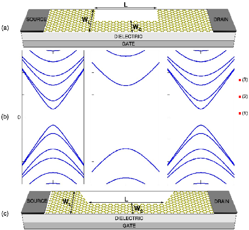
A way to get around the lack of reproducibility of current-voltage and transfer characteristics of CNTFET’s is to avoid the use of metallic electrodes close to the semiconducting channel. This has been attempted by integrating ohmic contacts in the carbon nanotube through a combination of back and top gatesJavey et al. (2004) which allow for an independent control of the density on different regions of the nanotube. This scheme allows to create metallic and semiconducting regions on a single nanotube. Band-gap engineering of graphene ribbonsNakada et al. (1996); Brey and Fertig (2006), on the other hand, offer an alternative strategy to the multiple-gate schemeHan et al. (2007); Pablo . A single graphene ribbon with armchair edges and a narrow constriction in the middle [see Figs. 1(a) and (c)] can present three regions with different band gaps which can be doped differently by a single back gate [see Fig. 1(b)]. For constriction widths with a number a dimer lines , with an integer smaller than the constriction presents a transport gap at room temperatureSon et al. (2006) and acts as the semiconductor active channel in standard transistors. Since the gap scales inversely with the width of the ribbon, the wide sections of the ribbon will always present a zero or vanishingly small gap. These can easily behave as metallic eletrodes or leads because of finite temperature or as they are driven out of the charge neutrality point by the action of the back gate voltage, . The same gate voltage controls the on-off state by bringing the Fermi level into the gap of the constriction or out of it [see Fig. 1(b)]
Theoretically, this system should behave as an ambipolar transistor where the threshold voltage, , is determined solely by the width of the constrictionFernandez-Rossier et al. (2007). The on-conductance, , and the subthreshold swing, , magnitudes that determine the transistor performace, are also controled by the capacitive couplings and by the atomic structure of the lead-constriction contact. The ultimate performace limits of graphene ribbon field effect transistors (GRFET’s) are here established for two contact models. The first, square, where the crystallographic orientation of one edge changes by 90∘ at the contact [see Fig. 1(a)]. The second, tapered, where the lead narrows down progressively until reaching the constriction width. This is achieved in practice by a single change in the crystallographic orientation of one of the edges of 60∘ [see Fig. 1(c)]. In this case the armchair edge is never interrupted, except for the change in the crystallographic orientation. The constriction is always placed laterally, i.e., on one side of the ribbon. This choice can be justified on the basis that, in order to fabricate a constriction with reduced disorder, it is desirable to leave untouched one edge of the initial graphene layer or wide ribbon and, e.g., etch away only the other edge (constrictions created by etching both edges have already been fabricatedHan et al. (2007)). Our proposed GRFET could simplify the fabrication process and might improve the final performance. A second justification will be mentioned when discussing the results.
Methodology.– We compute the conductance of the constriction, , using the Landauer formalism which assumes coherent transport across the constriction. The electronic structure is calculated in the standard one-orbital tight-binding modelNakada et al. (1996); Fujita et al. (1996); Brey and Fertig (2006); Muñoz Rojas et al. (2006); Fernandez-Rossier et al. (2007) which has been shown to reproduce the low-energy physics of ribbons whose edges are saturated with hydrogen. The scattering problem is solved using the Green’s function approach. This involves (i) the calculation of the Green’s function projected on the constriction and on part of the left and right ribbon, (ii) the calculation of the self-energies for the semiinfinite ribbon leads by iterative solution of the Dyson equationMuñoz Rojas et al. (2006), and (iii) the subsequent evaluation of the transmission probability, , using the Caroli expressionCaroli et al. (1971). The details can be found in Ref. Muñoz Rojas et al., 2006. In order to simplify the discussion, we assume first semiinfinite graphene ribbons on both sides. The role played by the metallic electrodes is considered at the end, although one can anticipate that they should not affect the results as long as , where is the width of the bulk ribbon and is the width of the constriction at its narrowest point.
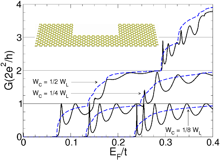
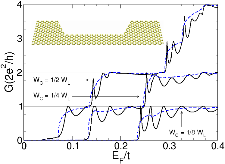
Zero-temperature results.– We begin by showing in Figs. 2 and 3 the zero-temperature for a constriction with length nm and 1/2, 1/4, and 1/8 , for =5.8 nm. For both types of contacts we obtain the expected step-wise increase of the conductance as a function of (in units of the hopping parameter ), associated with the increase in the number of bands crossing the Fermi level in the constriction. The steps come in pairs, reflecting the band structure of semiconducting armchair ribbons [see Fig. 1(b)]. On top of the steps we obtain strong Fabry-Perot-like oscillations as a consequence of the finite reflection at the constriction-lead contacts. The periodicity of these oscillations is consistent with the length and with the dispersion relation in the constriction. The amplitude of the oscillations, on the other hand, depends on how abrupt the contact is. For the square contact the amplitude of the oscillations is larger than for the tapered one, as expected. In order to separate the contribution of the scattering at the interfaces from the quantum interference effects, we have also computed the transmission of a single interface (dashed lines in Figs. 2 and 3). In all cases the transmission steps saturate to their quantum limit very slowly. For both contact types, as the width of the constriction decreases, the transmission worsens as a consequence of the increasing mismatch between lead and constriction wave functions. The increasing reflection on decreasing is somewhat damped for the tapered contacts, but still clearly visible. When quasilocalized states form in the constriction as a result of a significant loss in the transparency of the contacts. This situation resembles the formation of quantum dots in poorly contacted carbon nanotubesBockrath et al. (1999), but without metallic contacts. In general one can anticipate that constrictions with tapered contacts to the leads should perform better than their square counterparts for both and , although the overall performace diminishes as the constriction narrows down in both models.
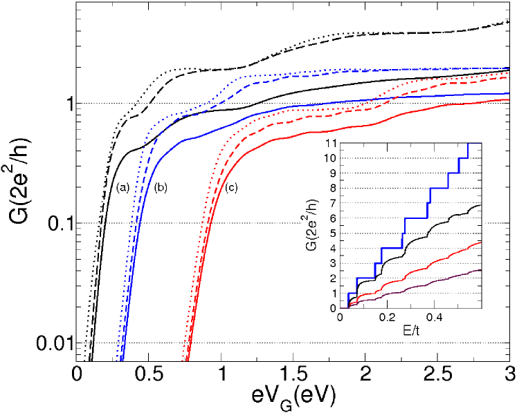
Room-temperature results.– We now turn our attention to the actual room-temperature performance of GRFET’s. Although the widths and lengths considered (nm) are still difficult to achieve with present lithographic techniquesHan et al. (2007), the results can be easily extrapolated to more realistic constrictions. The ones considered here behave as intrinsic semiconductors at room temperature since their gaps are in the range eV for a typical value of eV, which is much larger than meV at room temperature. Figure 4 shows a logarithmic plot of for the all the cases previously studied. In all cases the conductance oscillations have disappeared, smeared out by temperature. The exact relation between and depends on the actual capacitive couplings between graphene, gate, source, and drain electrodes. Modeling these couplings is beyond the scope of this workLiang et al. (2007). However, for wide and infinite ribbons where the source and drain electrodes are infinitely far away from each other an approximate analytic expression between and can be obtainedFernandez-Rossier et al. (2007):
| (1) |
where is the graphene lattice constant, is the dielectric constant, and is the capacitance ratio between graphene and graphene ribbonFernandez-Rossier et al. (2007). Here we have considered a realistic situation that reduces the classical electrostatic capacitance: nm, . Based on self-consistent calculations using the same methodology in Ref. Fernandez-Rossier et al., 2007, we estimate to be .
We can now extract the respective values of from the logarithmic plots. (Note that these values can be additionally taylored through , , and .) While, for the wider constrictions, is larger for the tapered contacts (90 vs. 74 meV/decade), these contacts outperform the square ones for the narrowest constrictions (125 vs. 132 meV/decade). In any case, increases as the constriction narrows down. Also, the combined action of the finite reflection at the interfaces, finite temperature, and tunneling prevents from reaching the quantum limit for before the next channel opens up.
The role of metal contacts.– Finally, to approach a real experimental situation, we consider the role played by the source and drain metallic electrodes which are needed to connect the ribbon to the external cicuitry. At room temperature, when the metallic electrodes are sufficiently far from the constriction, electrons may loose phase coherence before reaching it. In this limit we can consider the total conductance to be given by
| (2) |
where is the so-called four-terminal resistance of the constriction, and and are the four-terminal resistances (hereon considered equal) due to the contact with the source and drain metal electrode, respectively,
| (3) |
A new transmission function, , has been introduced to account for the scattering at the interface between the metal and ribbon. Finally, is the intrinsic quantum resistance of the ribbon. In this approximation the total conductance is given by
| (4) |
From Eq. 4 one can see that, under the initial assumption , the overall conductance is determined by the bare value calculated above. On the other hand, in the absence of scattering at both metal-ribbon interfaces and constriction, one recovers the perfect conductance of the ribbon. The function is, unfortunately, hard to determine and is expected to be strongly dependent on the metal used. ExperimentsHeinze et al. (2002); Javey et al. (2003); Yang et al. (2005); Chen et al. (2005) as well as first-principles calculations of this quantity for carbon nanotubesPalacios et al. (2003, 2007), have revealed that can range from 10-3 to 1. For Pd electrodes, which have proved to make excellent contacts, Javey et al. (2003); Palacios et al. (2007). For other metals this factor can be reduced in orders of magnitude. To illustrate the effect of the metal on the performace of the GRFET we consider an electrode model in the form of a bidimensional square lattice with the same hopping parameter as the graphene lattice and varying on-site energy, . The inset in Fig. 4 shows the conductance of a single metal-graphene interface for various . As an illustration, the inset in Fig. 4 shows for the square constrictions using . The performance of the GRFET’s is noticeably affected in all cases since close to . Scattering at the metal is, however, less effective in reducing down to close to as . All this results in the following. Scattering at the constriction increases as . On the other hand, the number of bulk ribbon channels at also increases as , reducing the pervasive effect of the contact resistance to the metallic electrodes. One can thus conclude that an optimal ratio will always exist for GRFET’s and that this ratio will depend on both the metal contact and type of constriction.
Final remarks.– When compared to bidimensional non-relativistic electronsSzafer and Stone (1989), the scattering at the constriction is much stronger in the case of relativistic ones. This prevents conductance quantization from appearing in these devices. For tapered interfaces, deviations from conductance quantization can still be of the order of 2 or 3% while they are of the order of 0.0001% for non relativistic electronsSzafer and Stone (1989). Our results support recent claims by KatsnelsonKatsnelson (2007), although more work is needed here to clarify these fundamental issues. When the constriction is placed symmetrically in the middle of the ribbon, the scattering at the contact turns out to be larger, strongly worsening conductance quantization and the performace of the GRFET. A detailed account of this and other possible contact models that can be considered will be published elsewherenoz Rojas et al. (2007).
Concerning disorder effects, a caveat should be issued. The use of of graphene ribbons for field effect transistors could be hampered by the fact that, in average, one out of three constrictions are metallic, given the unlikely chance that lithography can define the constriction with atomic precision. The same uncertainty in the lithographic definition of the constriction width, with the concommitant disorder at the edge, could, however, open up a gap, transforming otherwise metallic ribbons into a semiconducting onesSols et al. (2007).
In summary, our results show, generically, that the conductance of graphene ribbons with constrictions presents a step-like behavior as a function of or . However, one can hardly claim conductance quantization (in units of ) in most cases. At zero temperature, Fabry-Perot oscillations appear on top of the steps as a function of the gate voltage, being more pronounced for the square constrictions. Such oscillations result from finite scattering at the interfaces, which is reduced for the tapered ones, but not completely absent as naively expected. At room temperature, the Fabry-Perot oscillations disappear even for square interfaces and very short constrictions of nm. Due to the relativistic nature of electrons in graphene, does not saturate to the quantum limit close to for neither type of constrictions considered. However, from an operational point of view and compared to making direct contact to metal electrodes, one could say that tapered contacts between a graphene ribbon and a side constriction can perform nearly as ohmic contacts for intermediate constriction widths.
Acknowledgements.– F.M.R. is endebted to D. Jacob for his help with the transport code
and acknowledges the University of Alicante for financial support.
We acknowledge F. Guinea and P. Jarillo-Herrero for discussions.
This work has been funded by Spanish MEC under grants FIS2004-02356 and MAT2006-03741,
by Generalitat Valenciana under grant ACOMP07/054, and by FEDER Funds.
References
- Heinze et al. (2002) S. Heinze, J. Tersoff, R. Martel, V. Derycke, J. Appenzeller, and P. Avouris, Physical Review Letters 89, 106801 (2002).
- Javey et al. (2003) A. Javey, J. Guo, Q. Wang, M. Lundstrom, and H. Dai, Nature (London) 424, 654 (2003).
- Yang et al. (2005) M. H. Yang, K. B. K. Teo, W. I. Milne, and D. G. Hasko, Applied Physics Letters 87, 253116 (2005).
- Chen et al. (2005) Z. Chen, J. Appenzeller, J. Knoch, Y.-M. Lin, and P. Avouris, Nano Letters 5, 1497 (2005).
- Javey et al. (2004) A. Javey, J. Guo, D. Farmer, Q. Wang, D. Wang, R. Gordon, M. Lundstrom, and H. Dai, Nano Letters 4, 447 (2004).
- Nakada et al. (1996) K. Nakada, M. Fujita, G. Dresselhaus, and M. S. Dresselhaus, Phys. Rev. B 54, 17954 (1996).
- Brey and Fertig (2006) L. Brey and H. A. Fertig, Physical Review B 73, 235411 (2006).
- Han et al. (2007) M. Y. Han, B. Ozyilmaz, Y. Zhang, and P. Kim, Physical Review Letters 98, 206805 (2007).
- (9) B. Özyilmaz, P. Jarillo-Herrero, D. Efetov, D. A. Abanin, L. S. Levitov, P. Kim, arXiv:0705.3044v1 [cond-mat.mes-hall].
- Son et al. (2006) Y.-W. Son, M. L. Cohen, and S. G. Louie, Physical Review Letters 97, 216803 (2006).
- Fernandez-Rossier et al. (2007) J. Fernández-Rossier, J. J. Palacios, and L. Brey, Physical Review B 75, 205441 (2007).
- Fujita et al. (1996) M. Fujita, K. Wakabayashi, K. Nakada, and K. Kusakabe, Journal of the Physical Society of Japan 65, 1920 (1996).
- Muñoz Rojas et al. (2006) F. Muñoz Rojas, D. Jacob, J. Fernández-Rossier, and J. J. Palacios, Phys. Rev. B 74, 195417 (2006).
- Caroli et al. (1971) C. Caroli, R. Combescot, and P. Dederichs, J. Phys. C: Sol. State Phys. 4, 916 (1971).
- Bockrath et al. (1999) M. Bockrath, D. H. Cobden, J. Lu, A. G. Rinzler, R. E. Smalley, L. Balents, and P. L. McEuen, Nature (London) 397, 598 (1999).
- Liang et al. (2007) G. Liang, N. Neophytou, M. S. Lundstrom, and D. E. Nikonov (2007), arXiv:0705.0556v1 [cond-mat.mes-hall].
- Palacios et al. (2003) J. J. Palacios, A. J. Pérez-Jiménez, E. Louis, E. SanFabián, and J. A. Vergés, Phys. Rev. Lett. 90, 106801 (2003).
- Palacios et al. (2007) J. J. Palacios, P. Tarakeshwar, and D. M. Kim (2007), arXiv:0705.1328v1 [cond-mat.mes-hall].
- Szafer and Stone (1989) A. Szafer and A. D. Stone, Phys. Rev. Lett. 62, 300 (1989).
- Katsnelson (2007) M. I. Katsnelson (2007), cond-mat/0703190.
- noz Rojas et al. (2007) F. Muñoz Rojas, J. Fernández-Rossier, and J. J. Palacios, unpublished.
- Sols et al. (2007) F. Sols, F. Guinea, and A. Castro-Neto (2007), arXiv:0705.3805v1 [cond-mat.mes-hall].