Diffusive and ballistic current spin-polarization in magnetron-sputtered L10-ordered epitaxial FePt
Abstract
We report on the structural, magnetic, and electron transport properties of a L10-ordered epitaxial iron-platinum alloy layer fabricated by magnetron-sputtering on a MgO001 substrate. The film studied displayed a long range chemical order parameter of , and hence has a very strong perpendicular magnetic anisotropy. In the diffusive electron transport regime, for temperatures ranging from 2 K to 258 K, we found hysteresis in the magnetoresistance mainly due to electron scattering from magnetic domain walls. At 2 K, we observed an overall domain wall magnetoresistance of about 0.5%. By evaluating the spin current asymmetry , we were able to estimate the diffusive spin current polarization. At all temperatures ranging from 2 K to 258 K, we found a diffusive spin current polarization of %. To study the ballistic transport regime, we have performed point-contact Andreev-reflection measurements at 4.2 K. We obtained a value for the ballistic current spin polarization of % (which compares very well with that of a polycrystalline thin film of elemental Fe). We attribute the discrepancy to a difference in the characteristic scattering times for oppositely spin-polarized electrons, such scattering times influencing the diffusive but not the ballistic current spin polarization.
pacs:
72.25.Ba, 73.43.Qt, 75.50.BbI Introduction
Recent advances in the research field of current-induced magnetization switching and current-driven magnetization dynamics,Mangin et al. (2006) as well as the developments in the hard disk drive industry to change the magnetic storage process to perpendicular magnetic recording cause a resurgence of interest in ultrathin film magnetic materials with out-of-plane magnetic anisotropy. One way to achieve this is to exploit magnetocrystalline anisotropy in an epitaxial film.Caro et al. (1998); Suzuki et al. (1999); Ishio et al. (2002) This upsurge in research interest in epitaxial material exhibiting a high perpendicular uniaxial anisotropy constant has been stimulated especially since sputter deposition now yields epitaxial thin films of an ordering quality comparable to molecular beam epitaxy.Schwickert et al. (2000); Barmak et al. (2004, 2005); Clavero et al. (2006) The very high values of now available lead to domain walls of a very narrow thickness , and this makes fundamental physical phenomena like magnetoresistance due to electron scattering at magnetic domain walls an easily measurable effect. Ravelosona et al. (1999); Yu et al. (2000); Marrows and Dalton (2004) After some early experimental work,Heaps (1934); Taylor et al. (1968); Berger (1978) domain wall scattering is undergoing something of a renaissance as materials preparation and nanofabrication technologies improve.Kent et al. (2001); Marrows (2005); Tanigawa et al. (2006); Lee et al. (2006)
This effect of an increased electric resistivity in the presence of magnetic domain walls in a ferromagnetic thin film was measured by Viret et al. for films of Ni and Co. Viret et al. (1996) This group developed a semiclassical model based on spin-mistracking as the electrons cross the wall, which they used to interpret their data. (This type of model was necessary since quantum mechanical reflection of electrons from a domain wall potential step will be extremely small unless the wall is of extreme abruptness.Cabrera and Falicov (1974a, b)) A more rigorous quantum mechanical model, based on a Hamiltonian employed to calculate giant magneto resistance in a spin-split system, was used by Levy and Zhang to treat the same physics. Levy and Zhang (1997) It is possible to use this model to determine the polarization of a diffusive current by measuring domain wall resistance.Marrows and Dalton (2004)
This paper concentrates on the electron transport properties of the epitaxial L10-ordered iron alloy FePt in both the diffusive and the ballistic regime. In particular, we have measured the spin-polarization of the current in two different transport regimes: diffusive and ballistic. The strong uniaxial anisotropy, arising from the high degree of long range chemical order in our ordered alloy epilayers, leads to a dense stripe domain structure with narrow walls. These give rise to an easily measurable magnetoresistance associated with the extra resistance as the electrons pass through these walls. By using the Levy-Zhang modelLevy and Zhang (1997), this can be used to infer the spin-polarisation of these diffusive current carrying electrons, which we find to exceed 80% at all temperatures from 2 K to 258 K. We also determined the ballistic current spin polarization by the widely used point contact Andreev-reflection (PCAR) method.Soulen et al. (1998); Strijkers et al. (2001) We found a spin polarization of %, close to that reported for elemental 3 ferromagnets.
II Sample preparation and characterization

The samples were prepared by conventional dc magnetron sputter deposition on polished MgO substrates. We used a 4%-hydrogen-in-argon sputter gas mixture to prevent any film oxidation during growth at high temperatures. The FePt magnetic thin film was sputtered by co-deposition directly onto the substrates at a substrate temperature of 1000 K and at a deposition rate of 0.1-0.2 Å/s-1. Here we will describe the properties of a 31 nm thick film, which has one of the highest degrees of chemical order we have achieved, having grown several dozen such samples to optimize our deposition process.
For structural characterization of the epitaxial L10-ordered FePt thin films, we carried out - x-ray diffraction scans using Cu- radiation in order to determine the long range order parameter according to
| (1) |
Here and are the atom fractions of the two components, and are the fractions of the lattice site types and in the ordered structure, and and are the fractions of each type of lattice site occupied by the correct types of atoms, on and on .Warren (1969); Macgillaury et al. (1962); Ibers and Hamilton (1974) A typical - scan of an L10-ordered FePt is displayed in Fig. 1. The presence of the (001) peak is normally forbidden by the structure factor for face-centered crystal lattices, and so its observation here confirms that there is preferential ordering on the alternating and planes. The -peak and -peaks were fitted with Lorentzian line shapes to yield the integrated intensities. Following the standard procedure, described in e.g. reference Warren, 1969, these integrated intensities, together with the peak positions, Lorentz polarization factors and atomic scattering factors, can be used to give a value for . We found for the particular film of thickness of 31.0 nm that we discuss in detail in this article, and routinely obtain in our sputtered films. We calculated the film thickness via Kiessig-fringes obtained in low-angle x-ray reflectometry measurements.
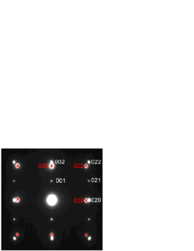
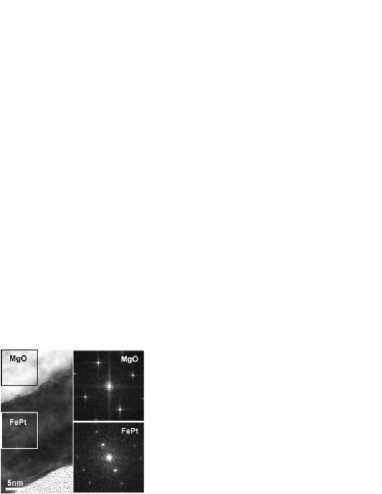
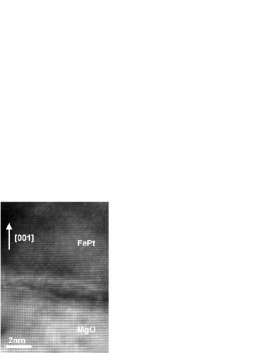
We performed transmission electron microscopy (TEM) on an FEI Tecnai F20 to provide structural information on our material.MacKenzie et al. (2005) The cross-sectional high-resolution transmission electron microscopy (HRTEM) image in Fig. 2 from a comparable sample, taken with the electron beam aligned parallel to the or zone axis of the MgO substrate confirms the high quality of our epitaxial FePt layers on the MgO(001) substrates. The L10-ordering of the FePt was verified by selected area electron diffraction, see Fig. 3, which shows the diffraction pattern from a cross-sectional TEM of the same sample of FePt on MgO(001). The high degree of alignment between the MgO and FePt structures is clearly depicted. The and reflections from the face-centered cubic MgO substrate are marked with red crosses and show the expected four-fold symmetry associated with the zone axis. The remaining reflections are from the FePt layer and index as the zone axis of L10-ordered face-centered tetragonal FePt. The presence of the superlattice spots confirms the L10-ordering of FePt. Using a lattice parameter of for MgO as a calibration, we obtain and for the FePt structure. This gives a lattice mismatch of between the MgO substrate and FePt layer. In Fig. 4 we show another image with a larger field of view. Fast Fourier Transform (FFT) patterns obtained from the boxed areas in Fig. 4, and shown as insets, confirm that the superlattice spots seen in the electron diffraction pattern are associated with the L10 order in the FePt layer.
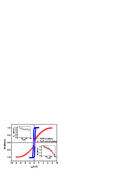
A quantitative analysis of the strong out-of-plane magnetic anisotropy of the L10-ordered FePt film was carried out by vibrating-sample-magnetometry (VSM) in the out-of-plane geometry as well as the in-plane geometry, with representative hysteresis loops shown in Fig. 5. The uniaxial magnetocrystalline anisotropy constant was calculated fromChikazumi (1998)
| (2) |
where the extra term accounts for the demagnetization field within the sample. and are the magnetic fields applied in and normal to the film plane respectively. For K, we found MJm-3, MAm-1, and fJm-1. We deduced the zero-Kelvin exchange stiffness from a -Bloch law fit of the temperature dependence of the saturation magnetizationChikazumi (1998) and assumed that follows a mean-field behavior : the data and fitted curve are shown in the lower right inset of Fig. 5. The temperature dependence of is shown in the upper left inset. Experimental micromagnetic data was not available for K due to the large signal that arises at low temperatures caused by paramagnetic impurities in the substrate (typically at the parts per million level in epi-ready MgO). The values we obtain compare reasonably well with the micromagnetic parameters recently reported for L10-ordered FePt thin films grown by molecular beam epitaxy and magnetron-sputtering of other groups. Farrow et al. (1996); Daalderop et al. (1991); Barmak et al. (2005); Clavero et al. (2006); Inoue et al. (2006); Okamoto et al. (2002).
We imaged the magnetic domain structure of FePt by magnetic force microscopy (MFM) at room temperature in zero field, as shown in Fig. 6 (a). The sample was demagnetized using an alternating magnetic field of decreasing amplitude. The cantilevers had a resonant frequency of 65 kHz and a spring constant of 1-5 N/m. The CoCr-coated Si tip was vertically magnetized prior to imaging. For optimal contrast we kept the tip-surface distance constant at a value in the range 20-25 nm. The average magnetic domain width of the demagnetized state was obtained by a power-spectrum analysis and resulted in a domain width of nm for the 31.0 nm thick sample. The domain structure exhibits the typical interconnected dense stripe domain structure known from L10-ordered binary iron alloys.Thiele et al. (1998); Barmak et al. (2005); Gehanno et al. (1997)
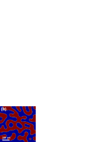
We carried out micromagnetic simulations of this domain structure in the sample using the oommf code,nist (1999) the results of which are shown in Fig. 6 (b). The cell size used was within the film plane and 15 nm perpendicular to the film plane, and a six-nearest-neighbor exchange interaction for the magnetic energy terms of adjacent cells was employed. Although thermal activation effects are not taken into account in this type of micromagnetic code, we were nevertheless able to simulate the domain structures in our material at finite temperatures using the appropriate values of the micromagnetic parameters , and as determined from vibrating-sample-magnetometry, as we are not concerned with thermal activation effects when determining the equilibrium domain structure. Our simulation yields an average domain width nm at room temperature for a 30 nm thick film obtained from a Fourier analysis of the oommf output. The analytical result obtained from the Kaplan-Gehring modelKaplan and Gehring (2000) is nm at room temperature and nm at 50 K, so the temperature dependence of the domain strip width is quite fairly weak.
We also estimated the average width of an individual domain wall analytically from
| (3) |
Using our experimentally determined micromagnetic parameters, we obtain 8-9 nm at all temperatures in good agreement with our micromagnetic simulations. Such narrow wall thicknesses are extremely difficult to measure experimentally. Such narrow Bloch-type domain walls may be found in many hard magnets materials such as NdFeB or SmCo. Their effect on thin film electron transport properties such as domain wall resistance is particularly interesting. Narrower walls are available only in a very few magnetic materials (e.g. at low temperatures in SrRuO3 Klein et al. (2000)).
III Electron transport properties
III.1 Transport in the diffusive regime
We first describe the diffusive transport properties of L10-ordered FePt. We performed magnetotransport measurements at temperatures ranging from 2 K to 258 K using an in-line 4-terminal set-up with the magnetic field applied normal to the film plane. We found a hysteretic part of the magnetoresistance of at 2 K and at 258 K, associated with the creation and annihilation of domain walls as the film switches its magnetization direction. A typical MR hysteresis loop is shown in Fig. 7. From previous studies on L10-ordered FePd thin films,Marrows and Dalton (2004) we know that a sufficiently high quality factor as similarly in this case, , is a good indication that the anisotropy magnetoresistance (AMR) contribution of Néel closure caps on the domain walls cannot account for this effect and is small enough to be neglected. The asymmetry of the MR loops arises through the extraordinary Hall effect, caused by large spin-orbit interaction in FePt, and the minute misalignment of our voltage probes. This effect can be easily subtracted to give the true domain wall MR. We will discuss the extraordinary Hall effect in films such as these in more detail elsewhere.
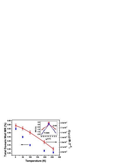
We find the domain wall MR to be approximately twice as large as compared to those reported on L10-ordered FePt films grown by molecular beam epitaxy,Yu et al. (2000) even though our film had a rather high electrical resistivity of cm (at 2 K) with at a residual resistivity ratio of . The temperature dependence of the domain wall MR is shown in Fig. 8 and exhibits an almost linear behavior with temperature. We observed a nearly complete suppression of any Köhler magnetoresistance () at high magnetic fields and low temperatures (Fig. 8), due to the high film resistivity giving rise to a very small value of . Hence, we attribute the much weaker effect of Köhler MR, as compared to FePd,Marrows and Dalton (2004) to considerably reduced electron mean free paths.
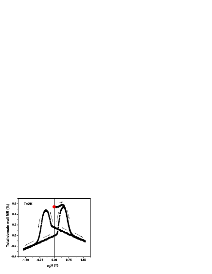
In addition to the hysteretic part of the MR we observe a reversible linear part at high fields. We have extracted the high field MR slopes at an applied magnetic field of 5 T at various temperatures (Fig. 8). In Fe, Co, and Ni, such a negative and linear MR was found by Raquet et al.Raquet et al. (2001) to be caused the influence of a magnetic field on the spin mixing resistivity. There, the main role is played by spin-flip - inter-band and intra-band scattering due to electron-magnon scattering. The data in Fig. 8 can be fitted with the expression given by Raquet et al. Raquet et al. (2002) quite well, with the exception that a substantial linear MR ( T-1) remains even at the lowest temperatures in this film, which must be added as an additional constant term. Subsequently, we could fit the temperature dependence of the high-field MR slope (Fig. 8) according to Raquet et al.Raquet et al. (2002). This procedure yields a magnon mass renormalization constant of , which is comparable with that of pure 3 metals,Stringfellow (1968), and less negative than that found previously in MBE-grown FePd.Marrows and Dalton (2004) We do not have a simple explanation for the temperature independent part of the high-field linear MR, although we note that magnetoresistances in thin films can take on a variety of unexpected forms.Pippard (1989)
Furthermore, we have used our magnetoresistance data to compute the spin-current asymmetry parameter in L10-ordered FePt based on the Levy-Zhang spin-mistracking model.Levy and Zhang (1997) The spin asymmetry of the current depends on the spin-resolved conductivities , (or spin-resolved resistivities , ) of the majority and minority spin channels and is given by
The Levy-Zhang model describes the MR only in the wall region, whereas we have measured our entire film. We estimated the volume fraction of walls by measuring the total wall length in the MFM image of scan width and multiplying this by the wall thickness to obtain the total area occupied by of walls, out of a total area of . This procedure yields a volume fraction accounting for the fact that we do not have a parallel stripe domain state, but rather a labyrinth structure, and yields a value approximately 1.3 times greater than the ideal stripe domain value . Thus one obtains for an isotropic labyrinth domain state a domain wall magneto-resistance ofMarrows and Dalton (2004)
| (4) |
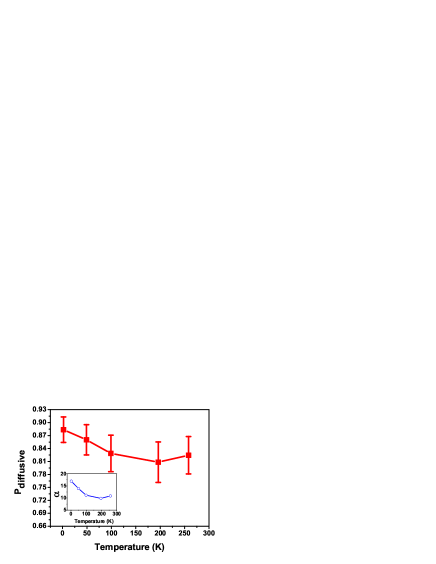
where is the Fermi wavevector, is the effective electron mass and is the Stoner exchange-splitting energy. It is to be noted that this formula yields the same for both and , equivalent to saying that we are insensitive to the sign of the polarization. Based on the assumption that the majority carriers are -like, we take to be equal to the free electron mass, assume the value of to be 2 Å-1 (a typical value for a metal), and take a value for the Stoner exchange splitting to be eV based on the splitting of the density of states seen in the results of band structure calculations.MacLaren et al. (2005) We appropriately scaled the domain wall volume fraction based on the analytical values for and for different temperatures. The inset of Fig. 9 shows the spin current asymmetry of L10-ordered FePt calculated according to Eq. 4. A strong temperature dependence of is clearly visible, with a decay of the spin current asymmetry from to in the temperature range between 2 K and 258 K. It is then straightforward to obtain the diffusive current spin polarization of L10-ordered FePt from
| (5) |
which is shown together with the spin current asymmetry in Fig. 9. For a temperature of 258 K, we found a diffusive spin current polarization of , whereas at K. The uncertainties in these polarization values are determined from the uncertainties in the -values, which in turn were computed using Eq. 4, and also taking into account the uncertainties of the micromagnetic parameters , and taken to evaluate the domain wall dilution. The final uncertainties are small since the diffusive polarization is rather insensitive to the value of when .
III.2 Transport in the ballistic regime
We performed point contact Andreev reflection (PCAR) measurements in order to directly probe for the ballistic current spin polarization of L10-ordered FePt.de Jong and Beenakker (1995); Soulen et al. (1998); Upadhyay et al. (1998); Strijkers et al. (2001); Nadgorny et al. (2001); Ji et al. (2001); Marrows (2005) The concept of this method is based on the fact that for applied bias voltages within the gap of the superconductor, it is physically impossible to inject or extract single electrons, but only Cooper pairs. As the Andreev reflection processAndreev (1988) is the coherent back reflection of a charge carrier hole into the ferromagnetic sample following the capturing of an opposite spin electron to form a Cooper pair inside the superconducting tip, one essentially probes for the number of unpaired electrons, straightforwardly giving the ballistic spin current polarization of the ferromagnet.
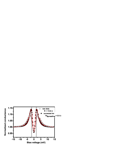
The point contact was controlled mechanically at 4.2K, in a liquid helium bath, between a superconducting niobium tip and the FePt thin film. We used the same sample as for the diffusive transport characterization. A bias voltage was applied across the point contact and the differential conductance was recorded via a four-probe technique. AC lock-in detection with a mV amplitude and a 5 kHz frequency was used. The tips were repeatedly brought into contact with the sample and the dependences of the differential conductance with the sample-tip bias voltage were recorded for various contact resistances. A typical curve is shown in Fig. 10. As also displayed in Fig. 10, the data were corrected from the contribution of spreading resistances within the film, as deduced from our measurements. Spreading resistances are commonly found when the resistances of the point contact (of around 10 in our case) are of the same order of magnitude as the resistance of the film (here around 80 ), and a common tell-tale sign is that the superconducting gap is significantly overestimated. It is then necessary to correct both voltage bias and differential conductance data for this additional series resistance.Woods et al. (2004) However, the effect of correction on polarisation is not large in our case, since the ratio of sub-gap to quasiparticle conductance never strays too far from unity at any value of bias, due to the polarisation is being close to 50 %.
From the typical resistances of the point contacts ranging between 4 and 15 , and using the Sharvin formula, we calculate an efficient point contact characteristic size of around 5 to 15 nm.Bugoslavsky et al. (2005); Woods et al. (2004) Such a value is much smaller than the characteristic micron-size of the terminated apex of our tip, as measured by scanning electron microscopy. Indeed, as it is usually the case, our contact results in multiple efficient nanometric point contacts,Bugoslavsky et al. (2005) where electron transport across the ferromagnet-superconductor interface is ballistic.
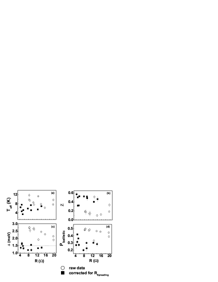
The conductance vs. bias voltage data were fitted in the standard way, employing a modified Blonder-Tinkham-Klapwijk (BTK) model Blonder et al. (1982), which describes the crossover from metallic to tunnel junction behavior of a microconstriction contact between a semiconductor and a superconductor based on the Bogoliubov equations. Four numerical fitting parametersStrijkers et al. (2001); Bugoslavsky et al. (2005) are employed to fit the measured conductance curves and thus determine the bulk current spin polarization of the sample: the effective temperature, ; the barrier strength, , which accounts for the cleanness of the interface (e.g. an infinite accounts for a tunnel transport regime); the superconducting gap, ( meV for elemental bulk niobium); and the spin polarization . The dependences of the fitting parameters on the point contact resistance () are plotted in Fig. 11, among with the resulting fits of the raw data, for comparison.
From the data shown in Fig. 11(a), it can be seen that on average is larger than the 4.2 K real temperature of the experiment.Strijkers et al. (2001); Kant et al. (2002) Such differences between effective and real temperatures have already been reported and are beyond the scope of this article. They are ascribed to weaknesses in the model since not only accounts for thermal activation but also includes other effects that result in a broadening of the Fermi-Dirac function such as the electron Fermi velocity mismatch between the tip and the sample or the presence of a thin remaining oxide layer at the surface. Moreover, this can also represent any spread in the properties of different parallel nanocontacts formed by the tip and sample. To avoid confusion, is sometimes referred to, in the literature, as a broadening factor.
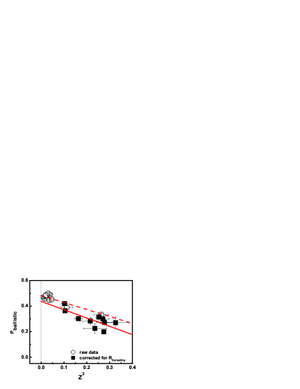
From the data shown in Fig. 11(b), it can be seen that for a given tip, there is no clear correlation between the point contact resistance and . It had been ascribed to the fact that for contacts of the same nature, is mainly determined by the size of the contact rather than its cleanness.Strijkers et al. (2001) As observed in Fig. 11(c), the values of the tips superconducting gaps are in agreement with those of the bulk Nb. Note that the initial large values of the superconducting gap as deduced from fits of the raw data are indeed the signature of spreading resistances. Figure 11(d) shows that the spin polarization does not depend on in an easily observable way. Rather note that the fitted spin polarization seems to systematically depend on . Here we find an acceptable agreement with a quadratic reduction in with ,Strijkers et al. (2001); Ji et al. (2001) as shown in Fig. 12. The relevant value of the spin polarization is known to be the one extrapolated in the case of a perfectly transparent interface (i. e. when ). We find a ballistic spin polarization of for our FePt film.
We note that we obtain similar values of the polarization when we do not apply any correction for the spreading resistance in our FePt film.Woods et al. (2004) This value is moreover close to that reported for elemental iron using the same technique, i.e. .Kant et al. (2002) We also note that we obtained the same value, to well within the error bar, when analyzing data taken on the sample in the remanent state or in the demagnetized state (not shown). It is actually not surprising, as this method is sensitive only to the magnitude and not the direction of the spin polarization. It is however important to notice that this shows that in this case the effect of any stray fields due to the domain structure on the superconductivity of the tip is negligible.
IV Discussion and Conclusion
We have determined both the diffusive and ballistic transport spin-polarization in high quality epitaxial sputtered L10 FePt thin films. In the diffusive electron transport regime, we used magnetoresistance of domain walls along with a modified form of the Levy-Zhang model to determine the spin current asymmetry and hence the diffusive spin polarization of a dc current flowing in L10 FePt. In the ballistic electron transport regime, we extracted the spin polarization directly from point contact Andreev reflection measurements at 4.2K.
Comparing the polarization in the ballistic transport regime to that in the diffusive, we find that at liquid He temperatures, where the comparison is direct, is substantially higher. In fact, to change the value of to be equal to that measured for by PCAR, it is necessary to change by a factor of a little over 24. This is because the diffusive polarisation is extremely insensitive to when it is large. Whilst the exact value can be modified by making a different choice for the value of or , it is not possible to get a value of that is close to with a physically reasonable set of parameters. To do so, it is necessary to choose a value for that is less than the free electron mass, extremely unrealistic for a transition metal alloy. With regards to , we chose as a representative value of for a metal. In order to obtain a value of to match the PCAR value of , we would need , corresponding to an electron density of about , three orders of magnitude too high for a metal, and placing the Fermi surface in the 4th Brillouin zone.
One would not expect that and should be the same in any case. It was pointed out by Mazin Mazin (1999) that for a fairly transparent ballistic contact, the conductivity for given spin sub-band , whilst for ordinary diffusive transport the conductivity . It is on these parameters that the spin polarization depends:Mazin (1999) compare equation 6 with equation 7. The ballistic current polarization is given by
| (6) |
On the other hand, taking into account spin-dependent electron scattering events within the Drude theory, the diffusive current polarization is given by
| (7) |
which involves a spin-dependent relaxation time , besides the
band structure parameters like the density of states and
the square of the Fermi velocity . Our work could act as a
stimulus for detailed band-structure calculations needed to average
and over the whole Fermi surface in order
to make quantitative comparisons, but we would like to note that the
scattering rate is seen to be the decisive parameter here.
It is not unreasonable to expect that in a ferromagnet such as this, where scattering
from defects and impurities occurs at different rates for carriers
of different spin.O’Handley (2000) Our parameters for scattering
within the FePt metal are within the range of those reported for
various impurities introduced as scattering centres into a 3d
magnetic matrix. Dorleijn (1976); Campbell and Fert (1982); van den Berg (2000)
Moreover, the parameter that appears in drift-diffusion
models of the current perpendicular to plane giant magnetoresistance
plays the role of the spin-polarization of the diffusive
conductivity within the bulk of a magnetic layer. Values for
of up to 0.9 have been found for some commonplace 3d ferromagnetic
alloys.Bass (1999) We therefore explain the much higher values
of as compared to as
arising from the asymmetry in the scattering rates for spin-up and
spin-down for scattering from vacancies, impurities, and anti-site
defects in the L10 structure, which lead to additional
polarization in the diffusive current over and above that from the
band structure alone. Meanwhile only the electronic structure
affects the polarization obtained from the PCAR method. It is worth
noting that even an unpolarized electron gas can carry a diffusive
current of finite spin-polarization in the presence of
spin-dependent relaxation times. Hence an appropriate ratio of
spin-dependent scattering rates can considerably amplify (or, in
unfavorable circumstances, attenuate) an intrinsic
spin-polarization in terms of number density when a current starts
to flow.
This is significant, since it is
that is the relevant parameter entering into theories of current
driven wall
motionTatara and Kohno (2004); Zhang and Li (2004); Li and Zhang (2004); Thiaville (2004, 2004); Tserkovnyak (2006); vanhaverbeke (2007); krueger (2007)
indeed it was in this context that Berger suggested, almost thirty
years ago, that a measurement of the pressure exerted on a wall in
ferromagnet could be used to determine current
polarisationBerger (1978). We expect that the results of this
measurement of should be in accord with that
measured by domain wall resistance. However, due to the dearth of
experimental data for diffusive values, when experimental data are
interpreted in terms of these theories, lower value of polarization
determined from a non-diffusive transport regime such as PCAR is
often the only available one to
useBeach (2006); Thomas (2006); Hayashi (2007); meier (2007). However, we
can see from the results in this article that these values
significantly underestimate the real degree of spin-polarization,
and hence the rate at which spin angular momentum is transferred to
a domain wall. We also anticipate that the diffusive current
polarization in more technologically relevant materials such as
Permalloy might be measured by making suitable nanostructures that
exploit geometrical confinement to form narrow domain
wallsBruno (1999) in order to yield a sufficiently large domain
wall resistance to be easily measured.
Acknowledgements.
The authors would like to thank A. T. Hindmarch, G. Burnell, M. Ali and M. C. Hickey for fruitful discussions. The technical assistance of J. Turton, M. Patel, L. Harris, A. Price, and B. Miller is also gratefully acknowledged. This work was supported by the UK EPSRC through the Spin@RT research programme. VB acknowledges the financial support provided through the European Community’s Marie Curie actions (Research Training Networks) under contract MRTN-CT-2003-504462, ULTRASMOOTH.References
- Mangin et al. (2006) S. Mangin, D. Ravelosona, J. A. Katine, M. J. Carey, B. D. Terris, and E. E. Fullerton, Nature Materials 5, 210 (2006).
- Caro et al. (1998) P. Caro, A. Cebollada, F. Briones, and M. F. Toney, J. Cryst. Growth 187, 426 (1998).
- Suzuki et al. (1999) T. Suzuki, N. Honda, and K. Ouchi, J. Appl.Phys. 85, 4301 (1999).
- Ishio et al. (2002) S. Ishio, T. Yoshino, H. Saito, T. Suzuki, and K. Ohuchi, J. Magn. Magn. Mater. 239, 217 (2002).
- Schwickert et al. (2000) M. M. Schwickert, K. A. Hannibal, M. F. Toney, M. Best, L. Folks, J.-U. Thiele, A. J. Kellock, and D. Weller, J. Appl. Phys. 87, 6956 (2000).
- Barmak et al. (2004) K. Barmak, J. Kim, L. H. Lewis, K. R. Coffey, M. F. Toney, A. J. Kellock, and J.-U. Thiele, J. Appl. Phys. 95, 7501 (2004).
- Barmak et al. (2005) K. Barmak, J. Kim, L. H. Lewis, K. R. Coffey, M. F. Toney, A. J. Kellock, and J.-U. Thiele, J. Appl. Phys. 98, 033904 (2005).
- Clavero et al. (2006) C. Clavero, J. M. García-Martin, J. L. C. Krämer, G. Armelles, A. Cebollada, Y. Huttel, R. A. Lukaszew, and A. J. Kellock, Phys. Rev. B 73, 174405 (2006).
- Ravelosona et al. (1999) D. Ravelosona, A. Cebollada, F. Briones, C. Diaz-Paniagua, M. A. Hidalgo, and F. Batallan, Phys. Rev. B 59, 4322 (1999).
- Yu et al. (2000) J. Yu, U. Rüdiger, A. K. Kent, R. F. C. Farrow, R. F. Marks, D. Weller, L. Folks, and S. S. P. Parkin, J. Appl. Phys. 87, 6854 (2000).
- Marrows and Dalton (2004) C. H. Marrows and B. C. Dalton, Phys. Rev. Lett. 92, 097206 (2004).
- Heaps (1934) C. W. Heaps, Phys. Rev. 45, 320 (1934).
- Taylor et al. (1968) G. R. Taylor, A. Isin, and R. V. Coleman, Phys. Rev. 165, 621 (1968).
- Berger (1978) L. Berger, J. Appl. Phys. 49, 2156 (1978).
- Kent et al. (2001) A. D. Kent, J. Yu, U. Rüdiger, and S. S. P. Parkin, J. Phys.: Cond. Matt. 13, 461 (2001).
- Marrows (2005) C. H. Marrows, Adv. in Physics 54, 585 (2005).
- Tanigawa et al. (2006) H. Tanigawa, A. Yamaguchi, S. Kasai, T. Ono, T. Seki, T. Shima, and K. Takanashi, J. Appl. Phys. 99, 08G520 (2006).
- Lee et al. (2006) W. L. Lee, F. Q. Zhu, and C.-L. Chien, Appl. Phys. Lett. 88, 122503 (2006).
- Viret et al. (1996) M. Viret, D. Vignoles, D. Cole, J. M. D. Coey, W. Allen, D. S. Daniel, and J. F. Gregg, Phys. Rev. B 53, 8464 (1996).
- Cabrera and Falicov (1974a) G. G. Cabrera and L. M. Falicov, Phys. Stat. Sol. (b) 61, 539 (1974a).
- Cabrera and Falicov (1974b) G. G. Cabrera and L. M. Falicov, Phys. Stat. Sol. (b) 62, 217 (1974b).
- Levy and Zhang (1997) P. M. Levy and S. Zhang, Phys. Rev. Lett. 79, 5110 (1997).
- Soulen et al. (1998) R. J. Soulen, J. M. Byers, M. S. Osofsky, B. Nadgorny, T. Ambrose, S. F. Cheng, P. R. Broussard, C. T. Tanaka, J. Nowak, J. S. Moodera, et al., Science 282, 85 (1998).
- Strijkers et al. (2001) G. J. Strijkers, Y. Ji, F. Y. Yang, C. L. Chien, and J. M. Byers, Phys. Rev. B 63, 104510 (2001).
- Warren (1969) B. E. Warren, X-ray Diffraction (Addison-Wesley, Reading, PA 1969, 1969).
- Macgillaury et al. (1962) C. H. Macgillaury, G. D. Rieck, and K. Lonsdale, eds., International Tables for X-ray Crystallography, Vol.III (The Kynoch Press, Birmingham, England, 1962).
- Ibers and Hamilton (1974) J. A. Ibers and W. C. Hamilton, eds., International Tables for X-ray Crystallography, Vol.IV (The Kynoch Press, Birmingham, England, 1974).
- MacKenzie et al. (2005) M. MacKenzie, J. N. Chapman, S. Cardoso, H. Li, R. Ferreira, and P. P. Freitas, J. Phys. D: Appl. Phys. 38, 1869 (2005).
- Chikazumi (1998) S. Chikazumi, Physics of Ferromagnetism (Oxford University Press, Oxford, 1998).
- Farrow et al. (1996) R. F. C. Farrow, D. Weller, R. F. Marks, M. F. Toney, A. Cebollada, and G. R. Harp, J. Appl. Phys. 79, 5967 (1996).
- Daalderop et al. (1991) G. H. O. Daalderop, P. J. Kelly, and M. F. H. Schuurmanns, Phys. Rev. B 44, 12054 (1991).
- Inoue et al. (2006) K. Inoue, H. Shima, A. Fujita, K. Oikawa, K. Fukamichi, and K. Ishida, Appl. Phys. Lett. 88, 102503 (2006).
- Okamoto et al. (2002) S. Okamoto, N. Kikuchi, O. Kitakami, T. Miyazaki, and Y. Shimada, Phys. Rev. B 66, 024413 (2002).
- Thiele et al. (1998) J.-U. Thiele, L. Folks, M. F. Toney, and D. K. Weller, J. Appl. Phys. 84, 5686 (1998).
- Gehanno et al. (1997) V. Gehanno, A. Marty, B. Gilles, and Y. Samson, Phys. Rev. B 55, 12552 (1997).
- nist (1999) M. Donahue, D. G. Porter, OOMMF User‘s Guide, Version 1.0, Interagency Report NISTIR 6376 (National Institute of Standards and Technology, Gaithersburg, 1999).
- Kaplan and Gehring (2000) B. Kaplan, and G. A. Gehring, J. Magn. Magn. Mater. 128, 111 (1993).
- Klein et al. (2000) L. Klein, Y. Kats, A. F. Marshall, J. W. Reiner, T. H. Geballe, M. R. Beasley, and A. Kapitulnik, Phys. Rev. Lett. 84, 6090 (2000).
- Raquet et al. (2001) B. Raquet, M. Viret, P. Warin, E. Sondergard, and R. Mamy, Physica B 294-295, 102 (2001).
- Raquet et al. (2002) B. Raquet, M. Viret, E. Søndergård, O. Cespedes, and R. Mamy, Phys. Rev. B 66, 024433 (2002).
- Stringfellow (1968) M. W. Stringfellow, J. Phys. C 1, 950 (1968).
- Pippard (1989) A. B. Pippard, Magnetoresistance in metals, Cambridge studies in low temperature physics (Cambridge University Press, Cambridge, 1989).
- MacLaren et al. (2005) J. M. MacLaren, R. R. Duplessis, R. A. Stern, and S. Willoughby, IEEE Trans. Magn. 41, 4374 (2005).
- de Jong and Beenakker (1995) M. J. M. de Jong and C. W. J. Beenakker, Phys. Rev. Lett. 74, 1657 (1995).
- Upadhyay et al. (1998) S. K. Upadhyay, A. Palanisami, R. N. Louie, and R. A. Buhrmann, Phys. Rev. Lett. 81, 3247 (1998).
- Nadgorny et al. (2001) B. Nadgorny, I. I. Mazin, M. Osofsky, R. J. Soulen, P. Broussard, R. M. Stroud, D. J. Singh, V. G. Harris, A. Arsenov, and Y. Mukovskii, Phys. Rev. B 63, 184433 (2001).
- Ji et al. (2001) Y. Ji, G. J. Strijkers, F. Y. Yang, C. L. Chien, J. M. Byers, A. Anguelouch, G. Xiao, and A. Gupta, Phys. Rev. Lett. 86, 5585 (2001).
- Andreev (1988) A. F. Andreev, Sov. Phys. JETP. 37, 5015 (1988).
- Woods et al. (2004) G. T. Woods, R. J. Soulen, Jr., I. Mazin, B. Nadgorny, M. S. Osofsky, J. Sanders, H. Srikanth, W. F. Egelhoff, and R. Datla, Phys. Rev. B 70, 054416 (2004).
- Bugoslavsky et al. (2005) Y. Bugoslavsky, Y. Miyoshi, S. K. Clowes, W. R. Branford, M. Lake, I. Brown, A. D. Caplin, and L. F. Cohen, Phys. Rev. B. 71, 104523 (2005).
- Blonder et al. (1982) G. E. Blonder, M. Tinkham, and T. M. Klapwijk, Phys. Rev. B. 25, 4515 (1982).
- Kant et al. (2002) C. H. Kant, O. Kurnosikov, A. T. Filip, P. LeClair, H. J. M. Swagten, and W. J. M. de Jonge, Phys. Rev. B. 66, 212403 (2002).
- Mazin (1999) I. I. Mazin, Phys. Rev. Lett. 83, 1427 (1999).
- O’Handley (2000) R. C. O’Handley, Modern magnetic materials : principles and applications (Wiley, New York, 2000).
- Campbell and Fert (1982) I. A. Campbell and A. Fert, Ferromagnetic Materials (North-Holland, Amsterdam, 1982), vol. 3, p. 747.
- van den Berg (2000) H. A. M. van den Berg, Magnetic multilayers and giant magnetoresistance: fundamentals and industrial applications (Springer-Verlag, Berlin, 2000), vol. 37 of Springer series in surface sciences, p. 215.
- Dorleijn (1976) J. W. F. Dorleijn, Philips Res. Rep. 31, 287 (1976).
- Bass (1999) J. Bass and W. P. Pratt, J. Magn. Magn. Mater. 200, 274 (1999).
- Tatara and Kohno (2004) G. Tatara and H. Kohno, Phys. Rev. Lett. 92, 086601 (2004).
- Zhang and Li (2004) S. Zhang and Z. Li, Phys. Rev. Lett. 93, 127204 (2004).
- Li and Zhang (2004) Z. Li and S. Zhang, Phys. Rev. Lett. 92, 207203 (2004).
- Thiaville (2004) A. Thiaville, Y. Nakatani, J. Miltat and N. Vernier, J. Appl. Phys. 95, 7049 (2004).
- Thiaville (2004) A. Thiaville, Y. Nakatani, J. Miltat and Y. Suzuki, Europhys. Lett. 69, 990 (2005).
- Tserkovnyak (2006) Y. Tserkovnyak, H. J. Skadsem, A. Brataas and G. E. W. Bauer, Phys. Rev. B 74, 144405 (2006).
- vanhaverbeke (2007) A. Vanhaverbeke and M. Viret, Phys. Rev. B 75, 024411 (2007).
- krueger (2007) B. Krüger, D. Pfannkuche, M. Bolte, G. Meier and U. Merkt, Phys. Rev. B 75, 054421 (2007).
- Beach (2006) G. S. D. Beach, C. Knutson, C. Nistor, M. Tsoi and J. L. Erskine Phys. Rev. Lett. 97, 057203 (2006).
- Thomas (2006) L. Thomas, M. Hayashi, X. Jiang, R. Moriya, C. Rettner and S. S. P. Parkin Nature 443, 197 (2006).
- Hayashi (2007) M. Hayashi, L. Thomas, C. Rettner, R. Moriya, Y. B. Bazaliy and S. S. P. Parkin Phys. Rev. Lett. 98, 037204 (2007).
- meier (2007) G. Meier, M. Bolte, R. Eiselt, B. Krüger, D. H. Kim and P. Fischer Phys. Rev. Lett. 98, 187202 (2007).
- Bruno (1999) P. Bruno Phys. Rev. Lett. 83, 2425 (1999).