A mechanism for unipolar resistance switching in oxide non-volatile memory devices
Abstract
Building on a recently introduced model for non-volatile resistive switching, we propose a mechanism for unipolar resistance switching in metal-insulator-metal sandwich structures. The commutation from the high to low resistance state and back can be achieved with successive voltage sweeps of the same polarity. Electronic correlation effects at the metal-insulator interface are found to play a key role to produce a resistive commutation effect in qualitative agreement with recent experimental reports on binary transition metal oxide based sandwich structures.
pacs:
85.30.Tv, 85.30.De, 73.40.-cResistive switching phenomena controlled by external voltages on metal-insulator-metal (MIM) sandwich structures is currently attracting a great deal of attention due the potential applications for non-volatile memory devices. The switching is an abrupt change between a highly resistive state (off state) and a conductive state (on state) driven by the applied voltage.
In recent years several MIM structures where the dielectric is a transition metal oxide (TMO) have been reported beck ; liu ; seo . After electro-forming, i.e., the application of large voltages in order to produce a permanent change in its electric properties, those systems exhibit large hysteresis in the - curves. In most cases reported so far the nature of the switching is bipolar, that is, if a system is switched from one state to the other by a pulse of a given polarity, then a pulse of opposite polarity has to be applied to switch it backbeck ; liu .
Surprisingly, several recent experiments on simple binary oxides (TiO2, NiO, CoO, etc.) demonstrated a novel switching effect seo ; rjung ; dsjeong06 ; dsjeong07 ; shima ; isao . In these systems the switching can be achieved by successive application of voltage pulses of the same polarity. While some qualitative ideas have been proposed, the origin of this so called unipolar switching phenomenon remains largely not understood.
Recently, we have proposed a phenomenological model that explains several aspects of the bipolar switching phenomena prl ; apl . The goal of this letter is to build up on that basic model and identify what additional hypothesis are required to account for the unipolar switching effect within the same framework. We anticipate that the key requirement is that the current injection during the high to low resistance transition (called SET) must be of short duration (see below).
The phenomenological model introduced in Refs.prl, ; apl, consists of an inhomogeneous dielectric medium connected to two electrodes (called top and bottom). The dielectric is conformed by two sets of small domains, each one in close physical proximity to the electrode interfaces, and also an additional large central domain that acts as a reservoir prl . Carriers move from domain to domain under the action of an electric potential. The hopping path of carriers can be associated to filamentary conduction across the dielectric. The domains may actually correspond to grains, dislocations, concentrated chemical inhomogeneities, such as vacancies or other type of defects rjung ; deac ; ventura06 ; ventura07 ; szot06 ; szot07 ; ddcuong ; fye . In the model they are simply characterized by the number of carriers that they can contain and their occupation at a given time. The model is further defined by the parameters that control the probabilities for the carriers to hop from domain to domain or to the electrodes. An important ingredient of the model is the effect of correlations apl . Since TMO are usually prone to strong correlation effects imada , we assume that under certain conditions that can be tuned by the electric pulsing, the interface (small) domains might undergo a metal-insulator transition. As a result, the density of states of those domains open a charge (Mott) gap, and their associated hopping probabilities get greatly modified. Since the affected domains are located at the interface, this effect has a significant impact on the conductance of the whole system.
Similarly as in Ref.apl, , here we adopt a simplified version of the model where the, in principle many, small “top” and “bottom” domains are represented by a single typical domain. Thus the model simply has only three domains: bottom, central and top. Since the systems are usually symmetric, following Refs. prl, ; apl, , we adopt the same hopping rates, , for the two interfaces [bottom(top) electrode - bottom(top) domain] and the same for all the internal hopping (domain - domain). The model is thus defined by the following three coupled non-linear differential equations apl ,
| (1) | |||||
| (2) | |||||
| (3) |
is the total number of states in electrode or domain , and is the occupation. denote “top-electrode”, “bottom-electrode”, “top”, “central” and “bottom”. The voltage dependent function actually gives a time dependence to the coefficients of the differential equation via the applied voltage protocol . This feature renders the system of equations very non-linear. A priori, the argument of these voltage dependent contribution to the hopping probabilities should be a fraction of the externally applied voltage, and a different one for each term in the equations above. However, for simplicity and to avoid a proliferation of model parameters, we shall assume that this dependence can be absorbed in the definition of the ’s. Explicitly, we adopt simmons where depends on various material parameters, and again, for the sake of simplicity, we set . Positive current is defined as carriers entering the bottom domain (or leaving the top domain). As in Ref.apl, we assume that the electronic state of the domains may undergo a metal-insulator transition. In practice, this may occur due to injection (leakage) of particles into (from) small domains, so that the occupation can trigger a density driven Mott metal-insulator transition, which is common in transition metal oxides imada . Alternatively, it may also occur due to a local electrochemical oxidation shima ; szot06 ; szot07 ; ogimoto ; stefanovich that is produced by the strong current densities during the electric pulsing. The oxidation is likely to occur near the electrodes at the small domains isao ; ybnian , and it would locally restore the originally insulating properties of the oxide. The phenomenon of local oxidation induced by a strong current has been observed in Ti films cilo .
Upon becoming insulating, the small domains open a charge gap in their excitation spectrum. We consider this effect explicitly in the model by modifying the appropriate in Eqs. to , where is temperature (more details are given below). Following apl we assume that domains are insulating when 1/2- 1/2+, ie, when their occupation is near half-filling with about one electron per site. We set .
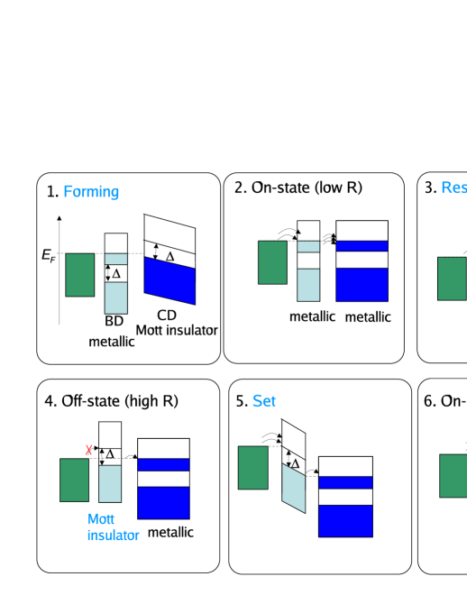
Within this model, a mechanism that produces the unipolar switching is schematically shown in the sequence of panels presented in Fig. 1. Similarly as in the case described in Ref.apl, , the switching effect is mostly controlled by either one of the two small domains rjung ; kmkim , which act as “electric faucets”isao . Here we shall assume that the bottom one is the relevant one, while the other remains conductive all the time.
Panel 1 schematically indicates the initial “electro-forming” step that is experimentally required. This process of soft breakdown is not described by our model. It involves the metalization of the initially dielectric bulk (central domain). We shall simply assume that forming sets the system in the state of panel 2, which is the initial state of our calculation. Thus, in panel 2, the system is in the conducting ON state (open faucet) where the small bottom domain (BD) is metallic with an occupation above 0.6. Upon application of a voltage pulse, the carrier hopping is enhanced and due to our assumption of , there is leakage from BD to the central bulk (panel 3). The leakage decreases the occupation of the BD until it reaches the threshold for the metal-insulator transition. At that point, the BD opens a gap in its band-structure and the hopping probabilities get reduced by a factor that enters in the renormalization , as described before. This metal-insulator transition is thus responsible of the RESET of the system that is now in the OFF state (panel 4).
To switch the system back to the low resistance state (SET transition) a new voltage pulse is initiated (panel 5). At low applied voltage a very small current circulates since the BD is insulating (closed faucet). As increases, a strong electric field develops across the BD. When the voltage at the electrode reaches a threshold value , such that the Fermi level of the electrode aligns with the bottom of the empty conduction band of the BD, a sudden injection of carriers occurs (panel 5). As this threshold is reached, the exponential factor in in the first term of the rhs of Eq.(1) disappears, and this dependent coefficient goes back to . It is important to realize that the second term of that equation remains unmodified as schematically shown in panel 5. At this point, the BD begins to increase its occupation and eventually the BD returns to the metallic state. This SET transition (open faucet) is very fast; it can be associated to a new local electric breakdown at the BD, as it occurs at a relatively high applied . Right after the transition, the large applied voltage produces a large current across the interface and, therefore, a rapid increase of the occupation of the small domain. Thus, to prevent the BD from leaking the carriers down to the central domain, the duration of the applied voltage pulse should be small. It is interesting to notice that this is reminiscent of the experimental situation, where the SET transition has to be performed with a current control dsjeong07 ; hosoi , which amounts to a rapid decrease of the applied as the device becomes conducting. After the BD returns to the metallic state (panel 6), the factor of the 2nd term of Eq.1 also returns to (open faucet) and the system goes back to the ON state of panel 2; a new cycle may then begin.
The SET process described in detail in the previous paragraph in which the system switches back from the OFF state to the ON state by application of a short voltage pulse of the same polarity as the initial reset pulse, is the key difference between this work and that of Ref.apl, .
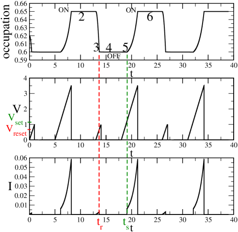
We now substantiate the previous qualitative description by solving the model equations following the considerations just described. In Fig.2 we show the occupation of the bottom domain as a function of time obtained by the action of six successive voltage pulses , all with positive polarity. In the top panel of Fig.2 the consecutive discharges and charges of the bottom domain are clearly observed. They can be correlated with the shown in the middle panel, where the thresholds for SET and RESET are indicated. The current entering the BD is shown in the lower panel, where the high current injection after the SET transition is clearly observed. On the other hand, due to the linear scale that we use, the low current level between and cannot be distinguished. To correlate the successive instants of the calculation with the previous qualitative discussion, we include in Fig.2 a number sequence that refers to the panels of Fig.1. We note that in the OFF state the occupation of bottom domain is smaller than 0.6, but only by an exponentially small amount which cannot be distinguished in the linear scale used. There is a certain freedom in the choice of the initial value of the occupation of the BD [the value =0.62 in Fig.2]. This arbitrary initial occupation would correspond to the initial state after the electro-forming process which is not described by the present model. Nevertheless, the important observation is that after the first sequence of RESET and SET pulses occurs, the initial condition is lost and the occupation , along with the memory operation, become cyclic.
To conclude, the behavior of our model is found to be in good qualitative agreement with the experimental reports of unipolar switching in transition metal oxide memories. We hope that our results provide a useful guidance for further experiments needed to improve our understanding of the basic switching mechanism in oxide non-volatile memories. The parameters of our model can be related to technologically important features such as switching speed and non-volatility. However their explicit calculation using ab initio methods, which would open the way for a multi-scale modeling of memory devices, remains a great challenge ahead.
Support from ECOS-Sud-Secyt, PICT 03-11609, PICT 03-13829 from ANPCyT, and Fundación Antorchas is acknowledged.
References
- (1) A. Beck et al., App. Phys. Lett. 77, 139 (2000).
- (2) S. Q. Liu, N. J. Wu, and A. Ignatiev, Appl. Phys. Lett. 76 2749 (2000).
- (3) S. Seo et al., App. Phys. Lett. 85, 5655 (2004).
- (4) R. Jung et al., App. Phys. Lett. 91, 022112 (2007).
- (5) D. S. Jeong, H. Schroeder, and R. Waser App. Phys. Lett. 89, 082909 (2006).
- (6) D. S. Jeong, H. Schroeder and R. Waser Electrochem. Solid-State Lett. 10, G51 (2007)
- (7) H. Shima et al., App. Phys. Lett. 91, 012901 (2007).
- (8) I. H. Inoue, S. Yasuda H. Akinaga and H. Takagi, preprint cond-mat/0702564.
- (9) M. J. Rozenberg, I. H. Inoue and M. J. Sánchez, Phys. Rev. Lett. 92, 178302 (2004).
- (10) M. J. Rozenberg, I. H. Inoue and M. J. Sánchez, App. Phys. Lett. 88, 033510 (2006).
- (11) A. Deac et al., J. Appl. Phys. 95,6792 (2004).
- (12) J. Ventura et al., J. Alloys and Compounds 423 181 (2006).
- (13) J. Ventura, Z. Zhang, Y. Liu, J. B. Sousa, and P. P. Freitas, J. Phys.: Condens. Matter 19 176207 (2007),
- (14) K. Szot, W. Speier, G. Bihlmayer, and R. Waser, Nature Materials 5, 312 (2006).
- (15) K. Szot, R. Dittmann, W. Speier, and R. Waser, Phys. Stat. Sol. (RRL) 1, R86 (2007).
- (16) D. D. Cuong et al., Phys. Rev. Lett. 98, 115503 (2007).
- (17) F. Ye et al., J. Appl. Phys. 101, 113528 (2007).
- (18) M. Imada, A. Fujimori and Y. Tokura, Rev. Mod. Phys. 70, 1039 (1998).
- (19) J. G. Simmons and R. R. Verderber, Proc. Roy. Soc. A 301, 77 (1967).
- (20) Y. Ogimoto, Y. Tamai, M. Kawasaki, and Y. Tokura, App. Phys. Lett. 90, 143515 (2007).
- (21) G. B. Stefanovich, C.-R. Cho, E.-H. Lee, I. K. Yoo, J. Non-Crystal. Solids 353 956 (2007).
- (22) Y. B. Nian, J. Strozier, N. J. Wu, X. Chen, and A. Ignatiev Phys. Rev. Lett. 98, 146403 (2007).
- (23) T. Schmidt, R. Martel, R. L. Sandstrom, and Ph. Avouris, Appl. Phys. Lett. 73, 2173-2175 (1998).
- (24) K. M. Kim, B. J. Choi, Y. C. Shin, S. Choi, and C. S. Hwang App. Phys. Lett. 91, 012907 (2007).
- (25) Y. Hosoi et al., Tech. Dig. —Int. Electron Devices Meet. (IEEE, New York, 2006), p.793.