Ultraviolet light emission from Si in a scanning tunneling microscope
Abstract
Ultraviolet and visible radiation is observed from the contacts of a scanning tunneling microscope with Si(100) and (111) wafers. This luminescence relies on the presence of hot electrons in silicon, which are supplied, at positive bias on - and -type samples, through the injection from the tip, or, at negative bias on -samples, by Zener tunneling. Measured spectra reveal a contribution of direct optical transitions in Si bulk. The necessary holes well below the valence band edge are injected from the tip or generated by Auger processes.
pacs:
68.37.Ef, 78.30.Am, 78.60.-b, 73.50.GrThe tip of a scanning tunneling microscope (STM) can be used to locally inject electrons or holes into a sample with atomic-scale precision and to excite the emission of light JIM . This emission has been observed and analysed from metals, adsorbed molecules and semiconductors KOEN ; ALV ; CDS ; USH ; MURA ; YOKO ; App05 . While on metals the light emission is excited in the tunneling gap region RB1 , the fairly intense luminescence from direct semiconductors has been shown to occur inside their bulk ALV ; CDS ; KOEN . Recently, tunneling-induced luminescence from Si(100), an indirect-band material, has been observed and attributed to inelastic transitions between Si dangling bond states and states specific to W tips Aono1 ; Aono2 . Very similar isochromat spectra were reported from - and -type material independently of the polarity of the tip-to-sample bias. Besides, the radiation from a STM contact with Si(111) has been reported and related to a localised plasmon which was suggested to arise on this Si surface Downes . Emission from the bulk of Si owing to the diffusing carriers was excluded. On the other hand, luminescence of bulk silicon is a known phenomenon HAY56 ; DUM57 , which is currently being used, e.g., in studies of metal-oxide-semiconductor (MOS) devices BUDE2 ; Vexler . A number of theoretical analyses have addressed the role of direct and phonon-assisted processes and of impurities BUDE2 ; PAV02 ; VIL95 ; CAR97 .
Here we undertake an experimental investigation into the STM-induced luminescence from - and -type Si. For the first time, detailed luminescence spectra are reported. We included both (111) and (100) orientations in our study, in order to vary the Si surface electronic structure, but the data suggests that this structure does not significantly affect the spectra. As will be shown further, our results are consistent with the model of radiative transitions within the bulk Si. In general, the luminescence of a STM contact has much in common with that of planar MOS structures. However, while the luminescence studies in MOS devices are limited to a low bias regime due to the oxide breakdown at elevated electric fields, this problem is less severe in STM experiments. As a result, we can observe the emission of ultraviolet photons with energies exceeding 4 eV.
The experiments were carried out in a custom built STM under ultra high vacuum conditions at ambient temperature THJ . Si samples (B doped p-Si(111), 1.5 cm; P doped n-Si(111), 56.5 cm; P doped n-Si(100), 10 cm) were prepared by resistive heating. NaOH etched and in vacuo heated tungsten tips were used. The photon detection setup was similar to the one reported in Ref. rsi, . A solid angle of 0.6 sr centered at ∘ with respect to the surface was detected. Light emission spectra were recorded on clean, reconstructed (77) Si(111) and (21) Si(100) surfaces. In all cases, they were corrected for the wavelength dependency of the detection sensitivity. The spectra were not noticeably affected by scanning the tip in a constant current mode. Since tip changes or surface damage are conveniently diagnosed during scanning we used this mode for spectroscopy and made sure that tip and surface remained unaltered.
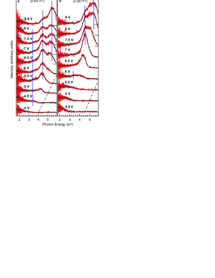
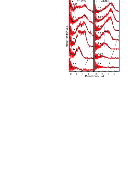
Series of luminescence spectra from p-Si(111) recorded at different sample voltages are presented in Fig. 1. For negative , clear peaks are observed at photon energies eV and 5.4 eV. An additional structure is discernible at eV for V. For positive , the peaks at eV and 5.4 eV were observed too, while at eV, enhanced intensity is hardly discernible except for the V data. Spectra from n-Si (Fig. 2) exhibit pronounced peaks at eV and 4.5 eV, but at 5.4 eV the intensity is only weakly perturbed. All the spectra show an intensity increase at low photon energies which is consistent with the luminescence of almost thermalized carriers observed also on Si MOS capacitors Yoder . No radiation was detected from the -Si samples for , unless we previously touched the Si surface with the W tip.
The observed peaks match the energies of direct interband transitions in Si as determined from reflectance and ellipsometry measurements ellipso ; reflect ; Zucca . Three sets of transitions can be identified MADEL : (a) and at eV, (b) , at eV, and (c) at eV. Some of these transitions, e.g. , involve holes with energies much lower than that of the valence band edge .
In this work we did not intend to perform detailed electrical or optical simulations considering the exact geometry of a STM contact. Instead, we restrict ourselves to a qualitative analysis and use models of a one-dimensional (planar) MOS tunnel structure. Such models allow to estimate the band bending in the semiconductor, the electron and hole components of the tunneling current through the insulator, the Zener current within silicon etc. and thus capture the essential physics. Note that the hole tunneling in a vacuum gap, oppositely to an oxide, occurs through the upper barrier formed by this gap, as there is no “insulator valence band”. Like in a regular MOS structure, the charge states of depletion, inversion and accumulation can be supported in a STM contact. An important difference between the planar and real topologies is that the depletion layer width for the given band bending value will be smaller than in planar case as can be verified from a calculation for a junction between a semiconductor and a metal sphere. When the sphere radius is large, the flat situation is imitated.
Below we use the energy diagrams of the tip-vacuum-semiconductor system, as if this system were planar, (Figs. 3,4) to illustrate the processes responsible for light generation.
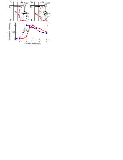
At positive sample bias, (Figs. 3a,b), electrons () are injected into Si with energies up to 9 eV above the conduction band edge of the quasineutral area. At such energies, Auger ionization processes are the predominant relaxation mechanism with a quantum yield around one Brodersen ; Vexler2 . The probability for the resulting hole to be created significantly below is high (e.g., for a 4.5 eV electron, the probability of generating a hole with an energy under eV exceeds Bude ). A second injected electron can then radiatively recombine with . These optical processes are localized at the depth of about ten nm in Si Yoder , so that a large fraction of emitted photons should reach the detector without reabsorption.
The above scenario is valid for both p- and n-type silicon. However, the energy of the injected electron with respect to and, therefore, the threshold for exciting a transition involving a specific conduction band state for a given bias voltage depends on doping (Fig. 3). Experimentally, such a variation is indeed observed. Fig. 3c displays isochromat spectra for the most intense spectral feature in the photon energy range () eV. The observed shift eV between spectra from - and -type Si agrees with the difference in bulk Fermi energies. This is strong indication that most of the photons are generated in the bulk material. For hypothetical near-surface transitions, should have reflected the band bending which is rather large and different for - and - Si.
At negative sample voltage, as already mentioned, the light was observed only for -Si. The absence of luminescence from -Si at is easy to understand. The junction operates at forward bias and the band bending is small. No hot electrons appear in the conduction band of silicon in such a case.
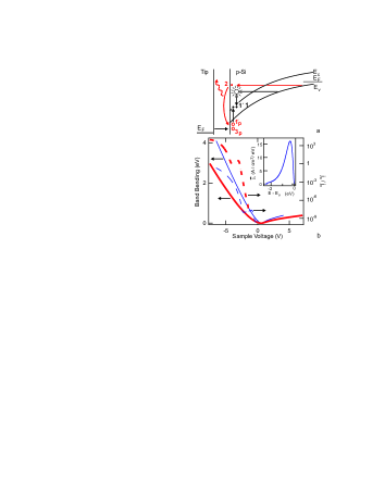
The origin of luminescence from -Si at can be explained as follows (Fig. 4a,b). The junction is reversely biased and strong band bending occurs. As a consequence, Zener tunneling of electrons from the valence band is possible; subsequently, these electrons are moving within the conduction band gaining high energy. Thus hot electrons and, via Auger transitions, hot holes are generated. An alternative process leading to the appearance of hot holes is tunneling between the tip and the states in Si underneath the valence band edge ( in Fig. 4a, inset to Fig. 4b). The final step is radiative recombination of with or with .
There might be doubts about the validity of a Zener transport mechanism in our relatively low doped -silicon samples. Indeed, this mechanism is known from the textbooks to come into the play at fairly high fields for which high dopant concentrations, say 1018-1019 cm-3, are required. However, one should not forget that these values refer to the planar geometry, and the same fields in the depleted region of a semiconductor may be attained in a STM contact topology even for much more moderate doping levels.
Fig. 4b (dashed lines) displays the calculated ratio of conduction and valence band current densities , where the acceptor concentration was taken larger than in our samples, to roughly compensate for the geometry effect. Qualitatively, at high negative bias, most hot holes are found to be provided by Zener tunneling followed by Auger processes, while hole injection from the tip becomes more significant for lower voltages. Note also that for a positive bias , Fig. 3, the role of valence band tunneling in supplying hot holes is always minor, since .
It is not useless to mention that ordinary MOS structures on highly doped -Si emit no light for , although Zener tunneling certainly occurs there. This may be due to the intense non-radiative scattering of hot electrons on defects in the presence of a large impurity concentration. In a STM contact, due to the difference in a topology, less highly doped samples can be used, which favors the observation of luminescence.
In summary, we have reported ultraviolet and visible light from Si(100) and (111) surfaces in a scanning tunneling microscope. While electron injection causes luminescence from - and -type samples, no emission is detected at negative sample bias from -Si in contrast to previous reports. We have presented the first detailed luminescence spectra revealing a great contribution of direct transitions of hot electrons and holes. The luminescence from -Si at reverse bias involves Zener tunneling and injection of holes well below the valence band edge.
Our results, in particular the similarity of the data from (100) and (111) surfaces, the spectral features observed, and the polarity dependence of the emission are not consistent with the interpretation of Si light emission in terms of localised plasmons Downes . They also are at variance with the interpretation of Refs. Aono1, ; Aono2, in terms of an inelastic transition between a specific W tip state and Si dangling bond states. It is important to note, however, that the dopant density of the Si samples used in Refs. Aono1, ; Aono2, was substantially higher than in our present work.
We thank P. Johansson, University of Örebro, for many discussions and for calculations of the electromagnetic response of a tunneling gap between a W tip and a Si surface. One of the authors (MIV) thanks the A. von Humboldt foundation for a support of his stay at the TU Braunschweig where part of this work has been done.
References
- (1) J. K. Gimzewski, B. Reihl, J. H. Coombs, and R. R. Schlittler, Z. Phys. B 72, 497 (1988).
- (2) Ph. Renaud and S. F. Alvarado, Phys. Rev. B 44, 6340 (1991).
- (3) R. Berndt and J. K. Gimzewski, Phys. Rev. B 45, 14095 (1992).
- (4) K. Ito, S. Ohyama, Y. Uehara, and S. Ushioda, Appl. Phys. Lett. 67, 2536 (1995).
- (5) T. Murashita, J. Vac. Sci. Technol. B 15, 32 (1997).
- (6) T. Yokoyama and Y. Takiguchi, Surf. Sci. 482-485, 1163 (2001).
- (7) M. Kemerink, K. Sauthoff, P. M. Koenraad, J. W. Gerritsen, H. van Kempen, and J. H. Wolter, Phys. Rev. Lett. 86, 2404 (2001).
- (8) I. Appelbaum, W. Yi, K. J. Russell, V. Narayanamurti, M. P. Hanson, and A. C. Gossard, Appl. Phys. Lett. 86, 063110 (2005).
- (9) R. Berndt, J. K. Gimzewski, and P. Johansson, Phys. Rev. Lett. 67, 3796 (1991).
- (10) C. Thirstrup, M. Sakurai, K. Stokbro, and M. Aono, Phys. Rev. Lett. 82, 1241 (1999).
- (11) M. Sakurai, C. Thirstrup, and M. Aono, Phys. Rev. Lett. 93, 46102 (2004).
- (12) A. Downes and M. E. Welland, Phys. Rev. Lett. 81, 1857 (1998).
- (13) J. R. Haynes and W. C. Westphal, Phys. Rev. 101 , 1676 (1956).
- (14) W. P. Dumke, Phys. Rev. 105 , 139 (1957).
- (15) M. I. Vexler, A. F. Shulekin, D. Grgec, I. V. Grekhov, and B. Meinerzhagen, Microelectron. Eng. 72, 180 (2004).
- (16) J. Bude, N. Sano, and A. Yoshii, Phys. Rev. B 45, 5848 (1992).
- (17) M. Pavesi, P. L. Rigolli, M. Manfredi, P. Palestri, and L. Selmi, Phys. Rev. B 65, 195209 (2002).
- (18) S. Villa, A. L. Lacaita, and A. Pacelli, Phys. Rev. B 52, 10993 (1995).
- (19) E. Cartier, J. C. Tsang, M. V. Fischetti, and D. A. Buchanan, Microelectron. Eng. 36, 103 (1997).
- (20) Th. Jürgens, Dissertation, Mathematisch-Naturwissenschaftliche Fakultät, Universität Kiel, Germany (2003).
- (21) G. Hoffmann, J. Kröger, and R. Berndt, Rev. Sci. Instrum. 73, 305 (2002).
- (22) P. D. Yoder, M. I. Vexler, A. F. Shulekin, N. Asli, S. V. Gastev, I. V. Grekhov, P. Seegebrecht, S. E. Tyaginov, and H. Zimmermann, J. Appl. Phys. 98, 83511 (2005).
- (23) D. Brust, M. L. Cohen, and J. C. Phillips, Phys. Rev. Lett. 9, 389 (1962).
- (24) A. Daunois and D. E. Aspnes, Phys. Rev. B 18, 1824 (1978).
- (25) R. R. L. Zucca and Y. R. Shen, Phys. Rev. B 1, 2668 (1970).
- (26) We use the notation from O. Madelung, Semiconductor-Basic Data, (Springer, Berlin, 1996).
- (27) C. Chang, C. Hu, and R. W. Brodersen, J. Appl. Phys. 57, 302 (1985).
- (28) I. V. Grekhov, A. F. Shulekin, and M. I. Vexler, J. Phys. Condens. Matter 7, 7037 (1995).
- (29) J. Bude, K. Hess, and G. J. Iafrate, Phys. Rev. B 45, 10958 (1992).