Multi-channel architecture for electronic quantum-Hall interferometry
Abstract
We propose a new architecture for implementing electronic interferometry in quantum Hall bars. It exploits scattering among parallel edge channels. In contrast to previous developments, this one employs a simply-connected mesa admitting serial concatenation of building elements closer to optical analogues. Implementations of Mach-Zehnder and Hambury-Brown-Twiss interferometers are discussed together with new structures yet unexplored in quantum electronics.
pacs:
72.25.-b,85.75.-d,74.50.+r,05.70.LnSince many decades interferometry has been a fundamental tool to disclose the classical and quantum properties of light MZ . Nowadays optical interferometry can be considered at the heart of a new quantum-based technology with applications in metrology METRO , imaging IMAGING , and quantum information processing OQC . In the solid state world, controlled quantum interference experiments appeared more recently when, thanks to the advances in fabrication, the wave-like nature of electrons could be tested in transport measurements. The observation of Aharonov-Bohm (AB) oscillations in the electric current RING and the Landauer-Büttiker formulation of quantum transport in terms of electronic transmission amplitudes lb signaled the beginning of quantum electronic interferometry in solid state devices. Since then, there has been a continuous effort in studying interference effect in quantum transport datta . A recent breakthrough in electronic interferometry has been the experimental realization of electronic Mach-Zehnder Ji03 ; neder ; litvin ; preden ; nedernaturep3 (MZ) and Hanbury-Brown-Twiss (HBT) neder2 interferometers using edge states in a quantum Hall bar. In these experiments electrons loop around an annular (Corbino-like) sample flowing along chiral edge channels which mimic the optical paths edgestate . In order to unfold the full potentiality of optical interferometry in the solid state realm an important additional ingredient is needed: The ability to concatenate in series several MZ interferometers. This requirement, impossible to implement at present, leads us to develop a new interferometric architecture for edge states. This scheme opens up a wide range of new possibilities in electronic interferometry. As first examples we discuss implementations of the MZ, HBT, and interaction-free Jang interferometers. Furthermore we show how to exploit our setup for characterizing the sources of dephasing in quantum Hall systems.
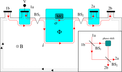
A good starting point to present our new architecture is to consider the MZ configuration. In an optical MZ interferometer (inset Fig. 1), a monochromatic beam from source a is split into two beams by a beam splitter BS1. The beams then propagate along two different paths which recombine at a second beam splitter BS2, where interference occurs. The two outgoing beams are collected at detectors a and b. In the absence of external noise, the beam intensity at the detectors exhibits oscillations as a function of the accumulated phase difference between the followed paths. Our electronic implementation of the MZ interferometer is sketched in Fig. 1. It consists of a 2DEG subject to a quantizing perpendicular magnetic field corresponding to a filling factor (number of occupied Landau levels) . Four electronic contacts are present in the structure: A bias voltage is applied to a, acting as a source, while the remaining contacts 1b, 2a and 2b are grounded. The shadowed regions in the figure represent top gates which reduce the local electron density in such a way that the filling factor in the underneath regions is . Such cross-gate technique, implemented e.g. in Refs. wurtz ; crossgate ; haug , is used to selectively address the two edge channels by introducing a spatial separation between them. In particular, the gate on top of a allows us to selectively populate only the outer edge of the sample by preventing the inner channel to be subject to the bias voltage . Analogously, the gate on top of the contact 2a allows us to measure the current carried by the outer edge channel only. Finally the large top gate in the center of the setup induces a spatial separation between the two edge states. The area defined by the two paths encloses a magnetic flux . It is important to notice that such an area can be substantially smaller as compared with other MZ realizations Ji03 ; neder ; litvin ; preden ; nedernaturep3 ; neder2 . In our proposed architecture values of m2 (corresponding to about flux quanta) are experimentally feasible with present technology. This is an improvement of almost two orders of magnitude with respect to conventional MZ setups that would arguably lead to a reduced effect of phase averaging due to area and/or flux fluctuations (as stated in Ref. neder2 , where a visibility enhancement was ascribed to a size reduction with respect to previous implementations Ji03 ).
Beam splitter transformations among the edges and are introduced, as in Ref. beenakker , by inducing elastic inter-channel scattering within the regions BS1 and BS2 of Fig. 1. This is admittedly the most delicate part of our proposal. There are however two ways to implement it. Inter-channel scattering can be obtained by an abrupt (non-adiabatic) variation in the confining potential such as the triangular-shaped protuberance shown in the figure. According to the calculations of Ref. palacios , edge channels mix coherently if the (potential defining) the protuberance shows spatial inhomogeneities on a scale smaller than the magnetic length . Such potential profiles can be engineered to give the desired scattering amplitude, for example, by the cleave-edge overgrowth technique ceo . Another possibility to have elastic inter-channel scattering is to use high-spatial-resolution local probes as atomic force microscopy woodside or scanning gate microscopy aoki . In this way there is the additional advantage that the scattering amplitudes can be tuned by means of an external voltage.
As in Refs. neder ; neder2 ; Ji03 ; litvin ; preden ; nedernaturep3 , we assume the size of the structure to be much smaller than the equilibration length at which spontaneous inter-channel mixing occurs haug . Moreover, apart from a small region where the BSs are implemented, the confining potential is assumed to be sufficiently smooth to prevent undesired inter-channel scattering. Under these conditions, and represent two independent electronic modes of propagation which play the role of optical paths in a MZ interferometer.
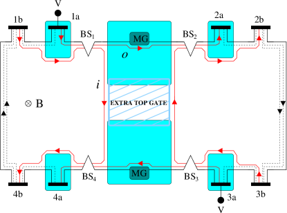
To have a first glimpse of the extreme versatility of this new architecture we notice that the setup of Fig. 1 can be turned easily into a HBT interferometer — see Fig. 2. The resulting implementation is reminiscent of the one realized by Neder et al. with the traditional (non simply connected) mesa configuration neder2 . In our case it has been obtained by introducing a further MZ interferometer in the bottom part of the mesa of Fig. 1, allowing the central top gates to overlap (possibly with the help of the extra top gate shown in the figure).
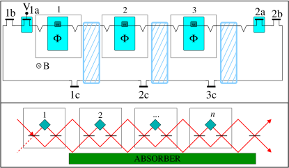
Additionally, very interesting devices with no counterpart in conventional edge state setups can be devised by fully exploiting the concatenability of our simply connected architecture. A first example is sketched in Fig. 3. This is an electronic equivalent of the optical interaction-free interferometer of Ref. Jang (see the caption of Fig. 3 for a brief description of its working principles). With our architecture we can reproduce it by properly concatenating a series of MZs of Fig. 1.
A further interesting application is found in the characterization of dephasing in quantum Hall systems which is recently attracting a lot of interest Ji03 ; neder ; litvin ; chung2 ; preden ; nedernaturep3 ; marquardt ; NEDERNJP . Consider first the setup of Fig. 1. The transmission probability from terminal 1a to 2a, reads
where for and , and are, respectively, the transmission and the reflection probabilities of the beam splitter BSj. A similar expression can be obtained for (transmission from 1a to 2b). The last contribution in Eq. (Multi-channel architecture for electronic quantum-Hall interferometry) is an interference term leading to current oscillations at the contact . It accounts for the phase difference associated to the two possible paths the electrons can choose in their propagation. Apart from an irrelevant constant term, in the absence of external noise it can be expressed as
| (2) |
The first term is a dynamical contribution given by chung2 , where is length difference between the paths (for simplicity we assume the channels and to have identical drift velocities). The second term in Eq. (2) is the AB contribution . Both the dynamical and the AB contributions can be varied in our setup by modifying the shape of the outer path by means of the local gate MG of Fig. 1. Decoherence can be described by adding an extra term in Eq.(2) which accounts for possible phase fluctuations. These may originate either from long time oscillations of locally trapped impurities or thermal fluctuations of the edge-state local density. Decoherence eventually leads to the suppression of the interference term in , Eq. (Multi-channel architecture for electronic quantum-Hall interferometry), thus reducing the visibility of the oscillations induced by the modulation of the gate MG in the output currents lb . Notably the visibility can be suppressed even in the absence of decoherence. This is due to the energy dependence of the phase, giving rise to a phase-averaging of the current when integrating over a large energy window chung2 . The visibility decrease has been intensively investigated in these systems Ji03 ; neder ; litvin ; chung2 ; preden ; marquardt ; NEDERNJP trying to identify its sources by means of shot noise measurement Ji03 . No information can be obtained just from the average current by using a MZ single interferometer. Our architecture makes possible to discriminate between phase-averaging and decoherence mechanisms directly in the measurement of the average current by concatenating two MZ interferometers.
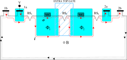
The setup is shown in Fig. 4. For the sake of simplicity we assume . The transmission between 1a and 2a for this device reads
with defined, as in Eq. (2), in terms of the parameters and associated with the two large gated areas of Fig. 4. The account for corresponding noise fluctuations. In the linear-response regime at zero temperature, contact 2a receives an output current with
Regarding decoherence, we treat it in a phenomenological fashion by defining a zero-temperature distribution of phase fluctuations , such that the average current reads . In the uncorrelated case [i.e. ] with Gaussian phase-fluctuations (of width ) we find
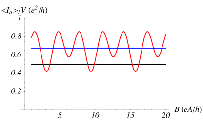
where , and . We see that has two interference terms proportional to and , respectively. The interference terms vanish only in the presence of full decoherence (): Strong phase averaging (large voltages) reduces to zero, but geometrical correlations between and can preserve from that (for instance, the case and yields ). This is strikingly different from the results of a single MZ interferometer, where complete phase averaging leads to the suppression of any interference term in the current and hence one has to resort to shot noise measurements. For illustration, we provide an example in Fig. 5. There we plot the linear conductance as a function of the magnetic field for small voltages (red curve) and for large voltages (blue curve) in the presence of a small decoherence (). Oscillations are suppressed as voltage increases due to the voltage dependence of . For large voltages (blue curve), the conductance converges to a constant value depending only on decoherence through . In the case of strong decoherence takes the universal value (black curve) showing no voltage dependence. A similar analysis was presented in Ref. Ji03 . In that case, shot-noise measurements were needed. It is also worth noticing that the configuration of Fig. 4 can be used to explore possible spatial correlations between the fluctuations in the two different MZ interferometers.
The architecture presented in this paper, once realized experimentally, may open up a way to an entire new class of electronic interferometry. We gave three examples, all based on the concatenation of several MZ interferometers. This proposal can be easily generalized to filling factors higher than , which would allow the implementation of complex multi-mode interferometry. This, along with the ability of multiple concatenation of interferometers, could yield prototypical implementation of simple linear-optics-like quantum computing OQC devices, or be relevant in revealing non-Abelian statistics in the fractional Quantum Hall regime law . Moreover, by properly tuning the BS transparencies, the setup of Fig. 1 yields a edge-channel swapper. Alternatively, it can be employed to prepare controlled superpositions of the two outgoing edge channels.
We thank M. Heiblum, F. Marquardt, V. Piazza and S. Roddaro for comments and discussions. We acknowledge financial support from the EU funded NanoSciERA “NanoFridge” and RTNNANO projects, and the “Ramón y Cajal” program of the Spanish Ministry of Education and Science.
References
- (1) M. O. Scully and M. S. Zubairy, Quantum Optics (Cambridge Univ. Press, Cambridge, 1997).
- (2) V. Giovannetti, S. Lloyd, L. Maccone, Science 306, 1330 (2004).
- (3) Y. Shih, Eprint arXiv:0707.0268.
- (4) E. Knill, R. Laflamme and G. J. Milburn, Nature 409, 46 (2001)
- (5) D. Y. Sharvin and Y. V. Sharvin, JETP Lett. 34, 272 (1981); R. A. Webb et al., Phys. Rev. Lett. 54, 2696 (1985).
- (6) M. Büttiker et al., Phys. Rev. B 31, 6207 (1985); M. Büttiker, ib. 38, 9375 (1988).
- (7) S. Datta, Electronic Transport in Mesoscopic Systems (Cambridge Univ. Press, Cambridge, 2005).
- (8) Y. Ji, et al., Nature 422, 415 (2003).
- (9) I. Neder, et al., Phys. Rev. Lett. 96, 016804 (2006).
- (10) L. V. Litvin, et al., Phys. Rev. B 75, 033315 (2007).
- (11) P. Roulleau, et al., arXiv:0704.0746 (preprint).
- (12) I. Neder et al., Nature Physics 3, 534 (2007).
- (13) I. Neder, et al., Nature 448, 333 (2007).
- (14) B. I. Halperin, Phys. Rev. B 25, 2185 (1982); M. Büttiker, Phys. Rev. B 38, 9375 (1988).
- (15) J. -S. Jang, Phys. Rev. A 59 2322, (1999).
- (16) R. J. Haug, et al., Phys. Rev. Lett. 61, 2797 (1988); S. Washburn, et al., ibid. 61, 2801 (1988).
- (17) R. J. Haug, Semicond. Sci. Technol. 8, 131 (1993).
- (18) A. Würtz, et al. Phys. Rev. B 65, 075303 (2002).
- (19) C. W. J. Beenakker, et al. Phys. Rev. Lett. 91, 147901 (2003).
- (20) J. J. Palacios and C. Tejedor, Phys. Rev. B 45, 9059 (1992); ibid. 48, 5386 (1993); O. Olendski and L. Mikhailovska, Phys. Rev. B 72, 235314 (2005).
- (21) L. Pfeiffer, et al. Appl. Phys. Lett. 56, 1697 (1990).
- (22) M. T. Woodside, et al. Phys. Rev. B 64, 041310 (2001).
- (23) N. Aoki, et al. Phys. Rev. B 72, 155327 (2005).
- (24) V. S. -W. Chung, P. Samuelsson, and M. Büttiker, Phys. Rev. B 72, 125320 (2005).
- (25) F. Marquardt and C. Bruder, Phys. Rev. B 70, 125305 (2004).
- (26) I. Neder and F. Marquardt, New J. Phys. 9, 112 (2007).
- (27) K.T. Law, Eprint arXiv:0707.3995.