Corresponding author: S. Burger
URL: http://www.zib.de/Numerik/NanoOptics/
Email: burger@zib.de
EMF Simulations of Isolated and Periodic 3D Photomask Patterns
Abstract
We present rigorous 3D EMF simulations of isolated features on photomasks using a newly developed finite-element method. We report on the current status of the finite-element solver JCMsuite, incorporating higher-order edge elements, adaptive refinement methods, and fast solution algorithms. We demonstrate that rigorous and accurate results on light scattering off isolated features can be achived at relatively low computational cost, compared to the standard approach of simulations on large-pitch, periodic computational domains.
keywords:
3D EMF simulations, microlithography, adaptive high-order finite-element method, FEMCopyright 2007 Society of Photo-Optical Instrumentation Engineers.
This paper will be published in Proc. SPIE Vol. 6730
(2007),
(Photomask Technology, R. J. Naber, H. Kawahira, Eds.)
and is made available
as an electronic preprint with permission of SPIE.
One print or electronic copy may be made for personal use only.
Systematic or multiple reproduction, distribution to multiple
locations via electronic or other means, duplication of any
material in this paper for a fee or for commercial purposes,
or modification of the content of the paper are prohibited.
1 Introduction
Rigorous electromagnetic field (EMF) simulations have become an important tool for mask design in low applications. As has been shown in previous works finite-element simulations are superior in terms of simulation accuracy, convergence rate and computation speed when compared to other presently used EMF simulation methods [1, 2]. We address 3D simulation tasks occuring in microlithography by using the frequency-domain FEM solver JCMsuite. This solver has been successfully applied to a wide range of 3D electromagnetic field computations including microlithography [1, 2, 3, 4], left-handed metamaterials in the optical regime [5], and photonic crystals [6]. The solver has also been used for pattern reconstruction in EUV scatterometry [7, 8], and it has been benchmarked to other methods in typical DUV lithography projects [1, 2].
In this paper we report on the current status of the finite-element solver JCMsuite, and we present simulation results of light transition through isolated and periodic features on photomasks.
2 Background
The finite-element package JCMsuite allows to simulate a variety of electromagnetic problems. It incorporates a scattering solver (JCMharmony), a propagating mode solver (JCMmode) and a resonance solver (JCMresonance). The scattering, eigenmode and resonance problems can be formulated on 1D, 2D and 3D computational domains. Admissible geometries can consist of periodic or isolated patterns, or a mixture of both. Further, solvers for problems posed on cylindrically symmetric geometries are implemented.
| layout setup | isolated | periodic | |
|---|---|---|---|
| set 1 | set 2 | set 3 | |
| [nm] | 260 | ||
| [nm] | 18 | ||
| [nm] | 55 | ||
| – | : : | m : 40 nm : m | |
| 400 nm | – | – | |
| 193.0 nm , coherent illumination, | |||
| 1.0 | |||
| N.A. | 1.0 | ||
| Magnification | 4 X | ||
| Rel. threshold | 0.69 | ||
In this paper we concentrate on light-scattering off 2D and 3D photomask patterns (lines and contact holes). The patterns of interest are isolated in the and directions and are enclosed by homogeneous substrate and superstrate (typically air) which are infinite in the -, resp. -direction. Cross sections through these patterns are schematically shown in Figures 1 and 2. We compare the results obtained from calculations on isolated computational domains to results from calculation on periodic computational domains with a large pitch. Cross sections through the periodic patterns are schematically shown in Figures 3 and 4.
Light propagation in the investigated systems is governed by Maxwell’s equations where vanishing densities of free charges and currents are assumed [9]. The dielectric coefficient and the permeability of the considered photomasks are complex and in the case of periodic mask layouts periodic, , . Here is any elementary vector of the periodic lattice. For given primitive lattice vectors and a periodic elementary cell can be defined as . In the isolated case the computational domain is choosen such that in the exterior domain only homogeneous or waveguide-like structures are present (see Fig. 2).
A time-harmonic ansatz with frequency and magnetic field leads to the following equations for :
-
•
The wave equation and the divergence condition for the magnetic field:
(1) (2) -
•
In the case of an isolated pattern: Transparent boundary conditions at all boundaries of the computational domain, , where is the incident magnetic field (plane waves in this case), and is the normal vector on :
(3) The operator (Dirichlet-to-Neumann) is realized with an adaptive PML method [10, 11]. This is a generalized formulation of Sommerfeld’s radiation condition.
-
•
In the case of a -periodic pattern: Transparent boundary conditions at the boundaries to the substrate (at ) and superstrate (at ), , according to Equation 3, and periodic boundary conditions for the transverse boundaries, , governed by Bloch’s theorem [12]:
(4) where the Bloch wavevector is defined by the incoming plane wave .
Similar equations are found for the electric field ; these are treated accordingly. The finite-element method solves Eqs. (1) – (4) in their weak form, i.e., in an integral representation.
The finite-element methods consists of the following steps:
-
•
The computational domain is discretized with simple geometrical patches, JCMsuite uses linear (1D), triangular (2D) and tetrahedral or prismatoidal (3D) patches. The use of prismatoidal patches is well suited for layered geometries, as in photomask simulations.
-
•
The function spaces in the integral representation of Maxwell’s equations are discretized using Nedelec’s edge elements, which are vectorial functions of polynomial order defined on the simple geometrical patches [13]. In the current implementation, JCMsuite uses polynomials of first () to ninth () order. In a nutshell, FEM can be explained as expanding the field corresponding to the exact solution of Equation (1) in the basis given by these elements.
-
•
This expansion leads to a large sparse matrix equation (algebraic problem). To solve the algebraic problem on a standard workstation linear algebra decomposition techniques (LU-factorization, e.g., package PARDISO [14], which was used in the simulations of Chapters 3, 4) are used. In cases with either large computational domains or high accuracy demands, also domain decomposition methods [15] are used and allow to handle problems with very large numbers of unknowns.
For details on the weak formulation, the choice of Bloch-periodic functional spaces, the FEM discretization, and the implementation of the adaptive PML method in JCMsuite we refer to previous works [10, 11]. In future implementations performance will further be increased by using curvilinear elements, general domain-decomposition techniques and -adaptive methods.
(a) \psfrag{(a)}{(a)}\psfrag{(b)}{(b)}\psfrag{(c)}{(c)}\includegraphics[width=195.12767pt]{epse/pitch_convergence} (b) \psfrag{(a)}{(a)}\psfrag{(b)}{(b)}\psfrag{(c)}{(c)}\includegraphics[width=195.12767pt]{epse/pitch_convergence_inset}
3 Rigorous simulations and large-pitch periodic-domain simulations of an isolated line
We apply the light-scattering solver of the programme package JCMsuite in order to simulate the lithographic projection of an isolated line.
The setup is as schematically shown in Figures 1 and 2, with geometrical, material, illumination and imaging parameters as in Table 1 (data set 1). We compare the obtained aerial image to results obtained with a setup of periodic lines of otherwise the same parameters, with a large ratio of pitch to linewidth (see Figures 3, 4 and Table 1, data sets 2, 3).
Figure 5 shows the simulation flow of the finite-element software:
-
•
The geometry of the computational domain is described in a polygonal format corresponding to Fig. 2 with material attributions and statements about the computational domain boundaries (periodic and transparent boundaries in this case). The translational vectors of the periodic pattern () are identified automatically from the layout, optimized settings of the perfectly matched layers (PML) are found automatically with an adaptive method (adaptive PML, aPML). Further, parameters specifying a maximum patch size of the finite-element mesh and further meshing properties can be set. From these geometry parameters and mesh parameters the mesh is generated automatically.
-
•
Material parameters (complex permittivity and permeability tensors) can be specified as piecewise constant functions and/or (using dynamically loaded libraries) as functions of arbitrary spatial dependence. In the presented example, the piecewise constant, isotropic settings given in Table 1 are used. The relative permeability is for all used materials.
-
•
Light sources can be defined as predefined functions (plane waves, Gaussian beams, point sources) or as arbitrary functions using dynamically loaded libraries. JCMsuite allows to generate solutions to several independent source terms in parallel, efficiently re-using the inverted system matrix. For the simulations in this chapter, without loss of generality, a coherent, polarized point source is used (wavevector ). For the simulations in Chapter 4, an unpolarized, incoherent source is used.
-
•
The main project definitions in this case are the accuracy settings (mesh refinement, PML refinement, finite-element degree) and the definitions of postprocesses. Upon execution the JCMsolve computes the full field distribution over the entire computational domain. Through internal or external post-processes, the quantities of interest can be derived from the field. E.g., the complex far field coefficients can be attained by Fourier integration / transformation and by the evaluation of the Rayleigh-Sommerfeld diffraction formula [16], an aerial image is calculated, or the field distribution is exported to graphics format for visualisation and analysis.
-
•
Interfaces to scripting languages like Python or MATLAB can be used for performing automatic parameter scans and data analysis. In the presented example, the interface for the generation of the input files and for the execution of a loop over the geometrical parameters given in Tables 1, 2 has been realized in MATLAB.
| layout setup | isolated | periodic |
|---|---|---|
| set 1 | set 2 | |
| [nm] | 240 | |
| [nm] | 300 | |
| [nm] | 18 | |
| [nm] | 55 | |
| 400 nm | – | |
| 400 nm | – | |
| – | nm : 40 nm : m | |
| – | ||
| 193.0 nm , incoherent illumination, | ||
| 1.0 | ||
From the obtained aerial image intensity distribution we decude a mask CD of the printed feature. For the specific parameter setting as given in Table 1 and from a simulation on the isolated computational domain we obtain a well converged value of the CD of approximately 65 nm. When we instead simulate the light distribution using periodic computational domains with large pitches we obtain some dependence of the CD on the pitch of the chosen computational domain. As expected, with increasing ratio of pitch to linewidth, the CD resulting from the aerial image at focal position with a fixed threshold (0.69 of the maximum intensity in this case) is converging to a fixed value for pitches well above 5 microns. This behavior is depicted in Figure 6. Please note that due to across-pitch imaging effects the resulting CD variation is rather large for a quasi continuously varied pitch (see, e.g. [17]), see the dotted line in Figure 6 (a). A smoother dependence is observed when the pitch is probed at multiples of wavelength times imaging magnification, see solid line in Figure 6 (a). However, also with this method, the waver scale CD error at a pitch-to-linewidth ratio of 10:1 is still of the order of 1 nm. Therefore, for accurate results on isolated features using a periodic model with large pitch-to-linewidth ratio, very large computational domains have to be chosen.
This demonstrates the advantages using the non-periodic model according to Fig. 2 and Equation 3. Using this model, the computational domain can be chosen just slightly larger than the feature of interest. The simulated aerial image still coincides with the aerial image from the periodic model with largest investigated pitch. This makes it possible to accurately compute images of isolated features with low computational effort (see singular data point for the isolated case in Figure 6 a,b).
4 3D isolated contact hole - near field convergence
In this chapter we investigate the application of our method to the simulation of light scattering off a 3D isolated contact hole. We concentrate on the convergence of the near field and – as in Chapter 3 – on the comparison to the large-pitch periodic case. Figure 7 shows a schematics of the geometrical layout: A contact hole with square shape of width and length (in mask scale dimensions) spans in the --plane. A cross-section in the --plane corresponds the linemask case, as depicted in Figure 2.
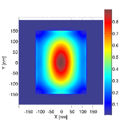
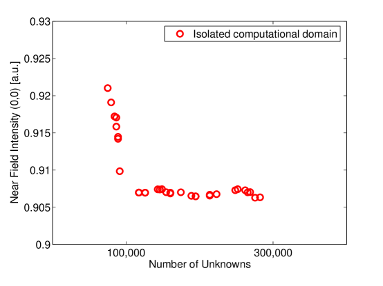
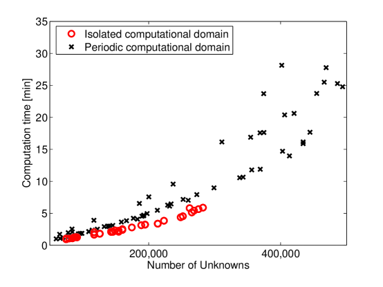
Figure 9 shows a -cross section through the obtained near field intensity distribution. The cross section is taken at constant position of , where corresponds to the upper edge of the upper chromium layer. The illumination in this case is an unpolarized, incoherent point-source at perpendicular incidence from the substrate. For the finite-element expansion and for the realisation of the PML boundary condition, fourth-order finite-elements have been used. The calculation has been performed on a standard 64-bit-CPU workstation with extended memory and several dual core processors (AMD Opteron). The computation time for this problem with about 100,000 unknowns is of the order of one minute. The convergence of the intensity is plotted in Figure 12. Here, fourth order finite elements are used, and simulations with different numbers of unknowns in the FEM expansion are reached by different spatial discretizations of the computational domain. Figure 13 shows the computational effort in minutes of total computation time in dependence of numbers of unknowns in the FEM expansion of the near field solution, . The values give only an estimate of the computational costs as upon the computations, the workstation has been used for other tasks in parallel. Typical memory (RAM) usage for the FEM computation of the solutions corresponding to the data points of this Figure is between 1 and 15 GigaByte.
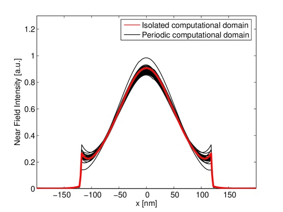
Figure 10 shows a 1D cross section through the intensity of the near field solution at constant and . Additional to the result obtained on the isolated periodic domain, results obtained on periodic domains are plotted in this figure. Due to typical computational resources limitations of full 3D computations the pitch in this case can not be choosen very large. Therefore the variation of the obtained field distributions in the investigated parameter regime is still of significant magnitude.
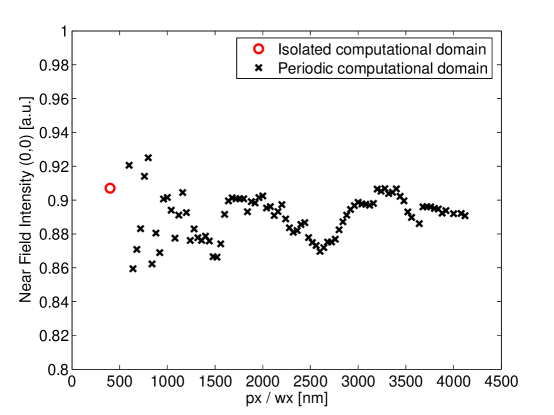
Figure 11 shows the intensity values corresponding to the data from Figure 10 at . As can be seen from the figure and as in the line mask case, a rather large computational domain has to be choosen when one tries to compute an accurate near field solution of an isolated contact hole on a periodic computational domain. The computational costs of the isolated and periodic computations as depicted in Figures 11 and 12 are shown in Figure 13. As can be seen from the Figures, an accurate solution where the field intensity at a specified position is converged with an error of lower than 0.5% can be reached with about 100,000 unknowns on the isolated computational domain. In contrast, with a large-pitch periodic model, the pitches in - and -direction have to be chosen very large to ensure that the model-induced error is neglectible. This leads to a very high number of unknowns in the FEM problem and consequently to a highly increased computational effort. Therefore, and especially for more complex isolated problems under investigation, a large-pitch periodic model is not a feasible option. This also holds for other discretization methods than FEM using periodic models for isolated problems. For the demonstrated 3D test problem the advantage of using isolated computational domains with transparent boundary conditions on all boundaries is more than one order of magnitude in computation time. With the implementation of this method rigorous and accurate investigation of scattering from isolated features has become straight-forward.
5 Conclusions
We have performed rigorous 3D FEM simulations of light transition through isolated features on linemasks and contact hole photomasks using the finite-element programme package JCMsuite. We have investigated the convergence behavior of the solutions and we have shown that we achieve results at high numerical accuracy. We have compared the results to calculations on periodic, large-pitch domains and found a performance advantage (cpu time) of at least one order of magnitude for calculations on isolated computational domains. Our results show that rigorous 3D simulations of isolated features on masks or wafers or in other settings can well be handled at high accuracy and relatively low computational cost.
References
- [1] S. Burger, R. Köhle, L. Zschiedrich, W. Gao, F. Schmidt, R. März, and C. Nölscher, “Benchmark of FEM, waveguide and FDTD algorithms for rigorous mask simulation,” in Photomask Technology, J. T. Weed and P. M. Martin, eds., 5992, pp. 378–389, Proc. SPIE, 2005.
- [2] S. Burger, R. Köhle, L. Zschiedrich, H. Nguyen, F. Schmidt, R. März, and C. Nölscher, “Rigorous simulation of 3D masks,” in Photomask Technology, P. M. Martin and R. J. Naber, eds., 6349, p. 63494Z, Proc. SPIE, 2006.
- [3] R. Köhle, “Rigorous simulation study of mask gratings at conical illumination,” Proc. SPIE 6607, pp. 6607–106, 2007.
- [4] S. Burger, L. Zschiedrich, F. Schmidt, R. Köhle, T. Henkel, B. Küchler, and C. Nölscher, “3D simulations of electromagnetic fields in nanostructures,” in Modeling Aspects in Optical Metrology, H. Bosse, B. Bodermann, and R. M. Silver, eds., 6617, p. 6617OV, Proc. SPIE, 2007.
- [5] S. Linden, C. Enkrich, G. Dolling, M. W. Klein, J. Zhou, T. Koschny, C. M. Soukoulis, S. Burger, F. Schmidt, and M. Wegener, “Photonic metamaterials: Magnetism at optical frequencies,” IEEE Journal of Selected Topics in Quantum Electronics 12, pp. 1097–1105, 2006.
- [6] S. Burger, R. Klose, A. Schädle, F. Schmidt, and L. Zschiedrich, “Adaptive FEM solver for the computation of electromagnetic eigenmodes in 3d photonic crystal structures,” in Scientific Computing in Electrical Engineering, A. M. Anile, G. Ali, and G. Mascali, eds., pp. 169–175, Springer Verlag, 2006.
- [7] J. Pomplun, S. Burger, F. Schmidt, L. W. Zschiedrich, F. Scholze, and U. Dersch, “Rigorous FEM-simulation of EUV-masks: Influence of shape and material parameters,” in Photomask Technology, 6349-128, Proc. SPIE, 2006.
- [8] Y. Tezuka, J. Cullins, Y. Tanaka, T. Hashimoto, I. Nishiyama, and T. Shoki, “EUV exposure experiment using programmed multilayer defects for refining printability simulation,” 6517, Proc. SPIE, 2007.
- [9] A. K. Wong, Optical Imaging in Projection Microlithography, SPIE Press, Bellingham, 2005.
- [10] L. Zschiedrich, R. Klose, A. Schädle, and F. Schmidt, “A new finite element realization of the Perfectly Matched Layer Method for Helmholtz scattering problems on polygonal domains in 2D,” J. Comput. Appl. Math. 188, pp. 12–32, 2006.
- [11] L. Zschiedrich, S. Burger, B. Kettner, and F. Schmidt, “Advanced finite element method for nano-resonators,” 6115, p. 41, Proc. SPIE, 2006.
- [12] K. Sakoda, Optical Properties of Photonic Crystals, Springer-Verlag, Berlin, 2001.
- [13] P. Monk, Finite Element Methods for Maxwell’s Equations, Claredon Press, Oxford, 2003.
- [14] O. Schenk et al., “Parallel sparse direct linear solver PARDISO.” Department of Computer Science, Universität Basel.
- [15] L. Zschiedrich, S. Burger, A. Schädle, and F. Schmidt, “Domain decomposition method for electromagnetic scattering problems,” in Proceedings of the 5th International Conference on Numerical Simulation of Optoelectronic devices, pp. 55–56, 2005.
- [16] L. Zschiedrich and F. Schmidt, “Evaluation of Rayleigh-Sommerfeld diffraction formula for PML solution,” in Proceedings of Waves 2007 - The 8th International Conference on Mathematical and Numerical Aspects of Waves, N. Biggs, ed., pp. 253–255, Univ. of Reading, UK, 2007.
- [17] B. W. Smith, “Forbidden pitch or duth-free: Revealing the causes of across-pitch imaging differences,” Proc. SPIE 5040, p. 36, 2003.