Evidence of the virtual Anderson transition in a narrow impurity band of p-GaAs/AlGaAs quantum wells: conductivity and electric breakdown at low temperatures
Abstract
In highly doped uncompensated p-type layers within the central part of GaAs/AlGaAs quantum wells at low temperatures we observed an activated behavior of the conductivity with low activation energies (1-3) meV which can not be ascribed to standard mechanisms. We attribute this behavior to the delocalization of hole states near the maximum of the narrow impurity band in the sense of the Anderson transition. Low temperature conduction is supported by an activation of minority carriers - electrons (resulting from a weak compensation by back-ground defects) - from the Fermi level to the band of delocalized states mentioned above. The corresponding behavior can be specified as virtual Anderson transition. Low temperature transport ( K) exhibits also strong nonlinearity of a breakdown type characterized in particular by S-shaped I-V curve. The nonlinearity is observed in unexpectedly low fields ( V/cm). Such a behavior can be explained by a simple model implying an impact ionization of the localized states of the minority carriers mentioned above to the band of Anderson-delocalized states.
pacs:
73.21.-bI Introduction
The problem of a conductivity via localized states was addressed during a long time; however it mostly concerned a hopping conductivity. At the same time experiment 1 ,2 ,3 demonstrated that a transition to metallic conductivity (or, in the case of 2D structures, to weakly localized conductivity) can occur within the impurity band still split from the conductance or valence band. Recent observation of superconductivity in B-doped diamond which was supported by the states of impurity band 4 once more stimulated an interest to the conductivity over localized states within strongly doped semiconductors.
Note that typically the situation of the compensated samples was studied where the Fermi level was situated in a region of large density of states. Metal-insulator transition in this case is associated with Anderson transition or, at least, with Mott-Anderson transition. As for the weakly compensated materials, until now a situation of the metal-insulator transition is not completely clear. Indeed, without a compensation a finite conductivity (including a hopping regime) can exist only via the states of the upper Hubbard band and in this case we deal with a ”pure” Mott transition. However a presence of even small number of compensating defects allows a finite hopping conductivity over single-occupied states. Indeed, in this case a few ”holes” within the impurity band, created by the compensating defects, are activated from the Fermi level to the maximum of the impurity band (nearest neighbor hopping). At the same time one can expect that if the concentration of dopants is large enough, then the carrier states within the impurity band become to be delocalized. Although the transport of the ”majority carriers” is still forbidden due to strong on-site correlations, the activated ”minority carriers” (arising from the compensating defects) can propagate as it would be in a metal. So we deal with ”virtual” Anderson transition: it happens in a situation where the delocalized states are still above the chemical potential, but the delocalized states do not exist until the concentration does not exceed some critical one. Since the disorder potential within the weakly compensated samples is weak enough, it allows to expect that such a ”virtual” Anderson transition can take place for the dopant concentrations sufficiently lower than for the Anderson transition for the ”majority carriers”. It is important that for 2D structures the compensating defects can be situated outside of the 2D layer which also decrease the disorder potential.
In the case of n-doped materials the ”majority carriers” within the impurity band are associated with electrons while the ”minority carriers” are associated with empty donors (”holes”). At the same time for p-doped materials the ”majority carriers” correspond to holes while the ”minority carriers” are related to negative acceptors, that is to electrons. It is important that the effective mass of the minority carriers is expected to be positive. Indeed, for the ”majority carriers” the impurity band is nearly completely occupied while the ”minority carriers” are situated close to the top of the corresponding energy band where the effective mass of the majority carriers is negative. Correspondingly, for the minority carriers the effective mass has the opposite sign with respect to the one of the majority carriers.
The scenario of the metal-insulator transition (of Mott type or of Anderson type) depends in real systems on the specific parameters of the material (compensation degree and related scale of the disorder potential, effective masses of the carriers etc. In general, the problem now is far from a complete understanding which makes corresponding studies to be actual.
In our recent publication 5 we reported an observation of activated conductivity at low temperatures in Be-doped uncompensated GaAs/AlGaAs single and multiple quantum wells with unusually small activation energies (more than an order of magnitude smaller than the Bohr energy of the dopant). It was shown that this temperature behavior can not be associated with nearest neighbor hopping ( conductivity). We attributed such a behavior to the ”virtual” Anderson transition mentioned above. Namely, we believe that the observed activation energy corresponds to activation of the ”minority carriers” from the Fermi level to delocalized states near the maximum of the impurity band. In the present paper we give detailed arguments in support of our conclusion including our new experimental results on low temperature low field breakdown effects observed in the samples demonstrating the behavior mentioned above. To the best of our knowledge, the breakdown behavior and S-shaped I-V curves observed in our experiments can not exist in the hopping regime. At the same time the scale of the electric fields (less than 10 V/cm) does not allow to relate these effects to breakdown to the valence band which would need much stronger electric fields.
II Experiment
The technique of growth of multilayered structures with a help of MBE method was described in our paper 6 . The structures contained 1,5,20 GaAs quantum wells with widths 15 nm separated by barriers of As with widths 100 nm. The middle region of the wells was doped by p-type impurities (Be), the volume impurity concentration was controlled during the growth and varied from atoms/cm3 up to atoms/cm3 (Table 1). The critical concentration for a bulk p-type GaAS is cm-3, i.e. the concentrations mentioned above are of the order or some less than the critical one. The compensation degree was sufficiently small and supposedly controlled by defects situated at the edges of the quantum wells and within the barriers. All the samples parameters are given in Table 1. The column gives the bulk acceptor concentration which was controlled during epitaxial doping.
| N | number of wells | well width, nm | ,meV | ,meV | |||
|---|---|---|---|---|---|---|---|
| 581 | 1 | 15 | 15 | 2 | 0,1 | ||
| 945 | 1 | 15 | 14 | 2,5 | 0,03 | ||
| 946 | 1 | 15 | 13 | 1,5 | 0,1 | ||
| 484 | 5 | 15 | 26 | 3 | 0,02 | ||
| 485 | 5 | 15 | 13, 26 | 2,5 | 0,03 | ||
| 200N1 | 20 | 15 | 25 | 2 | - | ||
| 200N2 | 20 | 15 | 16 | lnT | - |
The conductivity of heavily doped sample (200N2) at low temperatures weakly decreases with a temperature decrease which corresponds to weak localization regime and has been reported in 3 . Note that at high temperatures the samples demonstrated activated behavior of the conductivity and Hall effect with an activation energy meV (intermediate between and , where - is an energy of isolated acceptor in GaAs). Note that in the samples suffering Mott transition, is situated between the centers of the upper and lower Hubbard bands: , where - is the Hubbard energy which for 2D is lower than . Earlier we estimated the binding energy of doubly occupied state for the wells with a width 15 nm as 10 meV 6 , i.e. meV; it gives meV, which agrees with observed values of .
For the rest of the samples with concentration of acceptors close but still less than a critical one we observed a pronounced activated behavior of the conductivity at temperatures (10-1,3K) characterized by a low activation energy meV (Fig.1).
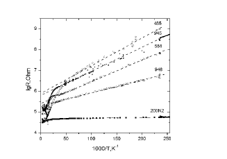
It was most pronounced for the single well structures. The value of decreased with an increase of acceptor concentration (samples 945,946 ). As it is seen from Fig. 1 and from the Table, the value of the preexponential was only by a factor 10 - 30 lower than the universal quantum limit for 2 D : . Fig. 2 demonstrates temperature behavior of the Hall mobility for these samples.
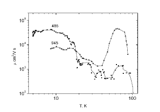
The maximum observed at high temperatures is attributed to a competition between scattering by optical phonons () and scattering by ionized impurities (. At temperatures 40-10 K one observes a further increase of with a temperature decrease. Such a behavior is not expected for the nearest neighbor hopping () since in the latter case the corresponding ”mobility” exponentially decreases with a temperature decrease 7 .
Now let us consider temperature behavior of the conductivity and Hall effect for these samples at high temperatures 20-300 . At there exist an activated behavior resulting from an activation of the holes from occupied impurity band to the valence band. The value of it is natural to ascribe to a distance from to the percolation level within the valence band. Since the degree of compensation is small, the width of the impurity band is also small and, as it will be shown below . Thus at small enough temperatures . However with the temperature increase when the value of the holes concentration starts to be of the order of the dopant concentration one expects a transition from the regime to the regime meV. It is this behavior which is observed experimentally (Table 1). This fact evidences that the low temperature behavior can not be attributed to conductivity.
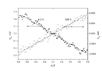
An important feature is related to the sign of the Hall coefficient. As it is clearly demonstrated (Fig. 3 ) the sign at 300 K is opposite to the sign at small temperatures.
At the same time the concentration estimated from the Hall coefficient appears to be 2-3 orders of magnitude lower than at K.
A specific attention was paid to the nonlinear effects in conductivity. Fig. 4 shows temperature behavior of resistance for different samples measured in a regime of constant current (0,1 - 2 nA).
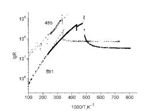
It is seen that at low temperatures the samples exhibit a sharp transition from insulating behavior (Arrenius law) to a metallic one; a magnitude of the resistance is decreased by 1.5-2 orders of magnitude. We believe that transition results from electric breakdown which takes place when the voltage drop on the sample (increasing with a temperature decrease) exceeds some critical value. The temperature of the transition differed for different samples and was equal to 3 , 2,4 , 2,1 . This parameter is supposedly controlled by the voltage drop at the given temperature which depends on the slop of temperature behavior of the conductivity.
Fig. 5 shows I-V curves of the samples (obtained in the regime of constant ) at different temperatures. The curves clearly demonstrate a presence of S-shaped regions. One notes that the breakdown takes place at relatively weak electric fields which can be estimated as less than 10 V/cm.
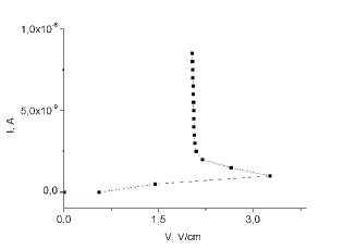
This breakdown can hardly take place in the regime of hopping conductivity. The hopping conductivity in finite electric fields was studied earlier for the similar group of samples 6 . As it has been shown, the hopping conductivity strongly (exponentially) increases with an electric filed increase, however this increase is still a gradual one and no breakdown-like behavior is observed (which agrees with theoretical predictions - see e.g. Shklovskii )
The breakdown can naturally result from an impact ionization of the acceptors to the valence band. However in this case the conductivity is expected to increase much larger than is observed experimentally. Then, for our case of relatively deep localized states, the breakdown would be expected at the fields at least orders of magnitude stronger than is observed experimentally (see e.g. Vorobev .
III Discussion
.
As it was noted earlier, the observed Hall mobility increases with decreasing temperature which excludes hopping conductivity as a mechanism leading to activated behavior of conductance at low temperatures and leads us to a conclusion that the activated minority carriers are delocalized. In this case the increase in the mobility with decreasing temperature can be explained by the scattering of delocalized carriers by acoustic phonons. This assumption does not contradict the fact that the mobility increases with temperature at high temperatures. We attribute this increase to the contribution of carriers activated to the valence band, where scattering on charged impurities prevails at corresponding temperatures. As known, scattering on acoustic phonons is very sensitive to the effective mass of the carriers. On the other hand, the effective mass of delocalized carriers in the impurity band can noticeably exceed the carrier mass in the valence band as, in particular, was shown in our paper [3], where this excess was estimated by a factor of 2-3. For this reason, the changes in the scattering mechanism and a character of temperature dependence of mobility can be expected with decreasing temperature.
There is another important evidence to support our picture which is related to the fact that a sign of Hall effect, observed at 4.2 K, is opposite to the sign of the Hall effect at 300K. The change of the sign apparently takes place at temperatures 20 - 40 K while the Hall data at these temperatures are not completely reliable.
Indeed, with an assumption of an existence of a band of delocalized states(BDS) within the narrow impurity band we conclude that there are 2 mobility edges separating the delocalized states from localized tail states. At low temperatures the conducting electrons are mainly concentrated near the bottom of the BDS where the effective mass of the electrons is expected to be positive since the corresponding density of states decreases with energy decrease.
Thus the Hall effect at high temperatures is produced by holes with positive effective mass while the Hall effect at low temperatures - by electrons with positive effective mass which explains the observed behavior.
Note that the effective mass of an electron near the opposite mobility edge (i.e. near the top of BDS) is expected to be negative. One has in mind that at high enough temperatures 20-50 K (which are larger than the activation energy ) all the electrons are expected to be distributed over the BDS with nearly equal probability and thus the net Hall voltage is expected to be small due to different signs of the effective mass at different parts of the BDS. It gives an alternative explanation of the behavior of Hall mobility which nearly vanishes at 20 -40 K but increases with temperature decrease when the contribution of electrons with positive effective mass start to dominate.
An important evidence supporting our scenario is given by the character of non-Ohmic behavior. The fact that the conductance in low-Ohmic state is still much less than high temperature conductance over the valence band excludes a breakdown to the valence band. Then, the electric fields in our experiments are orders of magnitude less than necessary for impact ionization of deep centers Vorobev .
In addition, extremely small electric powers (note that the breakdown behavior is observed at currents less than 1 nA!) do not allow any heating effects.
Thus we believe that the behavior observed results from the impact ionization of the electrons localized in the tail of the impurity band to the region of delocalized states. The important factor is a presence of a gap between the Fermi level at and the ”mobility edge” within the impurity band separating strongly and weakly localized states. This gap is filled by ”intermediate” localized states (see fig. 6) with a concentration much larger than the electron concentration.
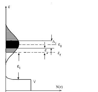
The electrons existing within the BDS (responsible for the impact ionization) with much larger probability can be trapped by these ”intermediate” states than by their initial centers. Since electron transport between the localized states is a hopping one, the return of the electrons to their initial position within the tail is suppressed. In its turn, the energy positions of these intermediate states are closer to the mobility edge than the tail states. As the result, the threshold field for the impact ionization from these intermediate states is lower that the threshold field for the ionization of the tails states. Correspondingly, the low-Ohmic state characterized by a presence of a finite electron concentration within the BDS can be supported at the electric fields which are lower than necessary for the ionization from the deep tail states which explains instabilities and S-shaped IV curves. (Note that the mechanism of a formation of S-shaped IV-curves related to a presence of ”intermediate” states between the ionized level and the conductance band was considered in Budsulak )
The detailed theoretical treatment supporting the scenario given above is given in the Appendix. We have taken into account both kinetics of impact ionization and nonequilibrium electron distribution in strong enough fields. The first critical field, according to our calculations, is given by the estimate
| (1) |
Here is an electron mean free path ( is transport relaxation time) while where is an electron-phonon relaxation time (note that both and correspond to electron energies equal to ). This equation has a clear physical explanation. The length is a length of electron diffusion during its inelastic relaxation time (controlled by phonons). Thus the critical field allows the energy gain from the electric field of the order of the energy , the latter is just the energy necessary to activate an electron from the Fermi level to the delocalized states.
The critical field is given by the similar equation, however the energy is in this case replaced by smaller energy corresponding to a typical distance from the electron trap states to the mobility edge. Thus we clearly have .
Now let us give a rough estimates of the parameters allowing the scenario mentioned above. Our sample exhibits an increase of mobility with temperature decrease nearly saturated at K at the values of the order of . The saturation demonstrates a change of scattering mechanism (supposedly from electron-phonon scattering to electron-defect scattering). Implying a value of g (which is several times larger than for the valence band) one estimates the transport relaxation time as s. To estimate one concludes that transport relaxation rate at the crossover temperature only by a factor is contributed by phonons. If we assume that characteristic electron energy is some less than this saturation temperature like meV, one concludes that s since . Then, for the energy meV one estimates the electron velocity as cm/s . Thus the critical field can be estimated as of the order of . The electric field is expected to be several times smaller, first, due to the fact that , then also due to a possible role of electron-electron scattering which can be effective at large enough concentration of the mobile carriers (see Appendix).
As it is seen from Fig. 5 , our rough estimates of the threshold field are in order of magnitude agreement with experimental results.
Then, from Fig. 3 it is seen that the conductance of the low-Ohmic state is of the order of the Ohmic conductance at K and is somewhat smaller than the conductance at intermediate temperatures 20 - 40 K (when the electrons are effectively activated to the BDS). This fact evidences, first, that we do not deal with impact ionization of the holes to the valence band (the resulting conductance would be of the order of the high temperature one which is several order of magnitude higher). Then, it shows that only a fraction of localized electrons is ionized to the BDS.
Note that the estimated threshold field is surprisingly low. We know only few references reporting S-shaped I-V curves at such a low fields, but for the case of shallow impurities [ ]. Since in our case we deal with relatively deep acceptors we can conclude that the observation of S-shaped I-V curves at low fields evidences a vicinity of metal-insulator transition which can not be of the Mott type. Indeed, it would contradict to the high-temperature activation energies which almost coincide with ionization energies of isolated acceptor while in a situation of the Mott transition Fermi level would be situated between energies of single occupied and doubly occupied states. In combination with the previous data it gives a strong support to the scenario of virtual Anderson transition. Then, it also allows to conclude that the observed conductivity can not be attributed to channel.
Thus, the results indicate that activation occurs to the band of the delocalized states appearing due to the Anderson transition in the impurity band. It is worth noting that the Anderson transition is typically considered in the single-particle picture in the absence of electron-electron correlations. In our case, the repulsion of holes from acceptors prevents transport of delocalized holes even if the wave functions in single-particle approximation are delocalized. However, owing to the activation of electrons from the Fermi level located at the tail of the impurity band to the indicated states, transport through such delocalized states becomes possible. In contrast to the real metal-insulator transition (when the Fermi level is located in the delocalized-state region), the manifestation of the delocalized states in our case can be described as the virtual Anderson transition. As we have shown earlier 5 , in the case of narrow impurity band existing in non-compensated samples due to the weak disorder potential the critical concentration of such a virtual Anderson transition is smaller than given by the Mott criterion by the factor
| (2) |
where is a width of the impurity band. Correspondingly, although the dopant concentration in our samples was less than the critical one for the real Mott-Anderson transition, it can readily be larger than the critical concentration for the virtual Anderson transition.
There is a peculiar question concerning localization according to Lifshits scenario Lifshits . Indeed, the scatter in inter impurities distances can impose localization as well as a scatter of energies and the corresponding criterion is except a numerical coefficient is similar to Mott criterion. However, first, the coefficient for the Lifshits transition is still unknown and we can expect that the Lifshits localization starts to be ineffective at lower concentrations than Anderson localization. Then, any deviation from purely random distribution of impurities (which can occur in course of doping procedure) suppress Lifshits localization.
To conclude, we have given experimental and theoretical evidences of an existence of virtual Anderson transition, characterized by an appearance of delocalized states within an impurity band above the chemical potential. Such a transition is expected to be typical for strongly doped, but uncompensated materials and precedes (as a function of dopant concentration) standard Mott-Anderson transition. In our experimental studies of highly doped uncompensated p-type layers within the central part of GaAs/AlGaAs quantum wells it manifested itself, in particular, in activated behavior of low temperature conductivity. We have shown that the latter can not be associated with known or mechanisms but results from an activation of electrons from the chemical potential to the delocalized states mentioned above. The fact that the type of the carriers in this case is different from the one supporting conductivity within the valence band is evidenced by a change of the sign of Hall coefficient with a temperature decrease. Another evidence of the virtual Anderson transition is given by electric breakdown observed at low temperature in unusually weak (for relatively deep centers) electric fields. We believe that this behavior is related to impact ionization of the localized electrons from below the chemical potential to the band of Anderson-delocalized states.
IV Acknowledgements
We are grateful to A.E. Zhukov for manufacturing the structures, to A.S. Ioselevich for discussion. This work was supported by the Russian Foundation for Basic Research (project no. 06-02-17068).
V Appendix
We consider impact ionization of localized ”minority” carriers - electrons - situated deep in the tail of the impurity band (with a concentration , controlled by compensating defects) by delocalized minority carriers to delocalized states with energies higher than the mobility edge (separating strongly and weakly localized states). We also have into account that in between and the position of the chemical potential at the equilibrium there exists a wide region of localized states which at low temperatures are occupied by holes and thus they can trap mobile electrons; the total number of such localized states is much larger than . While the analytical solution of the problem with continuous spectrum of the localized states seems to be impossible, we will model our system as the 3-level one, including the ”tail” states, the intermediate level of localized states separated from delocalized states by some energy , and the band of delocalized states.
Denoting the the number of electrons captured on the localized states as we describe the process of impact ionization at small temperatures as follows:
| (3) |
( is the coefficient describing a recombination of the electrons to any localized states, is the coefficient describing the recombination of electrons from intermediate states to their initial positions, is a coefficient of impact ionization, and are the coefficients describing the relative numbers of mobile electrons with kinetic energies larger than and , respectively.
Note that in principle the coefficients , are energy dependent. However we will neglect such a dependence since the width of the impurity band is not much larger than and thus the relative change of at energies higher higher than the threshold value is not large.
Analyzing the first of Eqs.V one concludes that since if initially , , this solution is stable with respect to small fluctuations up to threshold electric field corresponding to
| (4) |
At the same time for finite , the solution of Eq.V gives
| (5) |
Here we make use of the relations (which holds at electric fields of the order of ), , . This solution is stable until which holds until
| (6) |
which defines another critical field . Since it is expected that for a given field . Thus the value of can me smaller than and thus we deal with two branches of the solution: the one corresponding to , which is stable with respect to small fluctuations at and the solution given by Eq.V. For electric fields it corresponds to practically complete ionization of the electrons to the delocalized states. However this solution can exist at smaller fields until they are larger than , that is the two solutions coexist and are stable with respect to small fluctuations. We will give more detailed analysis later with an account of the fact that both the function and coefficients can be different for the two branches.
Now let us calculate the principal functions and . Considering the delocalized electrons we will take the mobility edge as the origin for . By definition
| (7) |
where as an electron distribution function.
We would like to emphasize that, strictly speaking, the electron transport in our situation can hardly be described in a same way as for standard energy band - at least in the vicinity of the mobility edge, so our simple equations can be considered as semiqualitative. For relatively small (when electron-electron processes are not effective) we will use a concept of energy diffusion and write with a neglect of electron-electron scattering
| (8) |
Here the first term describes a diffusion of an electron along energy axis due to interactions with thermal phonons with energies (phonon absorption and stimulated emission characterized by the relaxation time ) and due to energy gains and energy losses in course of chaotic motion in electric field,
| (9) |
is momentum relaxation time. The second term describes an energy drift along energy axis due to spontaneous emissions of phonons with typical frequency characterized by relaxation time . The electron-phonon relaxation for 2D electrons it is affected by the fact that the normal component of the phonon momentum is not conserved Karpus . According to Karpus at low temperatures which is similar to electron-phonon relaxation time in 3D metals and . At the same time for relatively small energies (where is a sound velocity while is an energy of lateral quantization which in our case of 2D impurity band is of the order of the Bohr energy) while .
The solution of Eq.8 depends on the relation between and phonon contribution to the energy diffusion. If the last term dominates, the solution corresponds to equilibrium, . If we have the opposite relation, which holds when
| (10) |
we deal with strongly nonequilibrium distribution
| (11) |
According to our experimental data on temperature dependence of the mobility, at the energy region of interest where and thus
| (12) |
This function is nearly constant at where
| (13) |
and extremely steeply (much stronger than simple exponential) decays at . As it is seen, for strong enough fields when the inequality of Eq.10 holds automatically.
For the further analysis we should have estimates for and . To estimate we have in mind that where is the ionization cross-section. The latter (in 2D) can be very roughly estimated as where is the geometrical cross-section of a Coulomb scattering of an electron with kinetic energy by a charged center, being a dielectric constant, is a cross-section of an elastic scattering of an electron by the trap center and is a typical electron wavelength which can be roughly estimated as where is a concentration of the delocalized states. Note that can be estimated from above basing on the known values of electron mean free path as (actually the corresponding cross-section can be smaller if electron momentum relaxation is dominated by other mechanism). As for we shall consider recombination due to phonon emission. In this case recombination process involves simultaneous interaction of an electron with phonon and trap center (neutral). One can estimate the recombination cross-section as .
Correspondingly, the estimates of the critical fields () can be rewritten as
| (14) |
Assuming that , one concludes that our scenario can hold provided
| (15) |
since in any case . As it can be readily estimated, cm while cm. Thus this criterion is obeyed for cm.
Since an equilibrium phase at corresponds to , the threshold field and, correspondingly, , is related to a distribution given by Eq.12 which can be modelled as a cut-off of of at . Correspondingly, . Thus can be estimated from an equality which gives
| (16) |
where , . Indeed, for and the condition of Eq.14 holds. Note that by definition coincides with the activation energy .
As it is seen, the estimate of is a similar one and we have because of the replacement of by in Eq.16.
If is high enough, the energy relaxation is dominated by electron-electron rather than by electron-phonon processes and thus
| (17) |
However the energy transfer from the electron system to the bath is still due to electron-phonon processes. The effective electron temperature which is established in the system can be derived from the energy balance between energy gain from electric field and its decay to the thermal bath . Thus we have
| (18) |
As it is seen from Eq.17 and Eq.13, formally the estimate for except of a numerical factor coincides with estimate for and characterizes an average electron energy which is controlled by energy balance between electrons and the lattice and does not depend on the efficiency of electron-electron processes. However the asymptotic behavior at large energies ( ) strongly depend on these processes. Namely, without these processes the decay of is significantly stronger within the region .
Let us assume that for electron concentrations electron-electron processes are much more effective for energy relaxation than electron-phonon ones. Thus the second branch (where ) corresponds to effective electron-electron scattering and electron distribution is described by Eq.17. Correspondingly, . Thus the electric field is given by the equation
| (19) |
However for the second branch where electron-electron scattering is assumed to be effective, we shall also consider Auger processes. Following the same rough procedure as applied above, we can estimate the cross-section as . Note that in this case Eq.V has a solution
| (20) |
and thus Eq. 6 holds automatically. However one has in mind that the Auger processes dominate only if
| (21) |
which holds only for large enough and is violated at some critical . At electron-phonon scattering dominates and the concept of electron temperature is not valid, so the system can not stay at the second branch. Thus the estimate of Eq.19 can be rewritten as
| (22) |
Note that the electron-electron processes can lead to additional source of multistability. Indeed, the concentration of high energy electrons given by Eq.17 can be at the same electric field larger than given by Eq.12. Correspondingly, the effective impact ionization by electron distribution of Eq. 17 can be supported at electric field somewhat weaker than necessary to support the distribution of Eq.12
References
- (1) D.A.Woodbury, J.S.Blakemore Phys.Rev. B 8, 3803, 1973
- (2) S.Liu, K.Karrai, F.Dummore, H.D.Drew, R.Wilson, G.A.Thomas Phys.Rev.B 48 , 11394, 1993
- (3) N. V. Agrinskaya, V. I. Kozub, et al., Piz. Zh. Eksp. Teor. Fiz. 80, 36 (2004) [JETP Letter 80, 30 (2004)]
- (4) T.Yokoya, T.Nakamura, T.Matsushita et.al. Nature 438, p.647, 2005
- (5) N. V. Agrinskaya, V. I. Kozub, and D. S. Poloskin, JETP Letters, 85, 169 (2007).
- (6) N. V. Agrinskaya, V. I. Kozub, Yu. L. Ivanov, et al., Zh. Eksp. Teor. Fiz. 120, 480 (2001) [JETP 93, 424 (2001)].
- (7) Yu. M. Galperin, E. P. German, and V. G. Karpov, Zh. Eksp. Teor. Fiz. 99, 343 (1991) [Sov. Phys. JETP 72, 193 (1991)].
- (8) B. I. Shklovskii, Fiz. Tekh. Poluprovodn. 13, 93 (1979) [Sov. Phys. Semicond. 13, 53 (1979)].
- (9) L.E.Vorob’ev, D.A.Firsov et.al. Pis’ma Zh. Techn. Fiz. 32, 9-34 (2006) [Technical Physics Letter 32, 384 (2006)]
- (10) E.Scholl Z. Phys B 46, 23 (1982)
- (11) I. M. Lifshits, Usp. Fiz. Nauk 83, 617 (1964) [Sov. Phys. Usp. 7, 571 (1965)].
- (12) V.Karpus, Fiz. Tekn.Polupr., 20, 12 (1986) (Sov. Phys. Semicond. 20, (1986)).