Field-tunable magnetic phases in a semiconductor-based two-dimensional Kondo lattice
Abstract
We show the existence of intrinsic localized spins in mesoscopic high-mobility GaAs/AlGaAs heterostructures. Non-equilibrium transport spectroscopy reveals a quasi-regular distribution of the spins, and indicates that the spins interact indirectly via the conduction electrons. The interaction between spins manifests in characteristic zero-bias anomaly near the Fermi energy, and indicates gate voltage-controllable magnetic phases in high-mobility heterostructures. To address this issue further, we have also designed electrostatically tunable Hall devices, that allow a probing of Hall characteristics at the active region of the mesoscopic devices. We show that the zero field Hall coefficient has an anomalous contribution, which can be attributed to scattering by the localized spins. The anomalous contribution can be destroyed by an increase in temperature, source drain bias, or field range.
keywords:
Intrinsic spin lattice, 2DEG, Spin interaction, Anomalous Hall effect, RKKYPACS:
72.25.-b , 71.45.Gm , 71.70.Ej, , , , , , and
1 Introduction
Experimental simulations of fundamental magnetic interactions on few spin basis are very challenging. The most common approach investigates the interaction between localized spins with the spin cloud of surrounding conduction electrons, where localized spins are created by using either atomic nucleii [1], intentionally embedded magnetic impurities [2], or odd electron quantum dots (QDs) [3, 4]. Individual localized spins can be employed to simulate the Kondo effect [3, 4]. In systems containing more than one localized spin, the spins can interact via the Ruderman-Kittel-Kasuya-Yoshida (RKKY) exchange with interaction parameter [5, 6]. This has been shown experimentally for the two-spin case, where the interaction has been tuned electrically with surface gates [7]. The pairwise coupling can be ferromagnetic for , or anti-ferromagnetic for . For non-interacting spins, , the Kondo effect contributes one additional state at each localized spin within a bandwidth of at . Non-equilibrium transport spectroscopy then shows a resonance in differential conductance at zero source-drain bias () [8, 9], which we call type-I zero bias anomaly (ZBA). With interacting spins , the resonance is suppressed at for , and , resulting in a split resonance, which we call type-II ZBA [10, 11, 12, 13]. The half width at half maximum of the split is defined as and acts as an indicator of spontaneous spin-polarization and static magnetic phases within the system [14, 10, 15].
Here we present high-mobility mesoscopic heterostructures that show signatures of an intrinsic spin lattice. As, in two dimensions, interspin distance , and tunes the exchange interaction parameter for [16, 13], we can tune the magnetic state of the spin lattice with a simple non-magnetic surface gate. The interspin distance is fixed for a given device, and can be evaluated via phase interference effects at low temperatures, or with commensurability effects at temperatures mK [13]. Such a system is ideal for investigations of magnetic phases in two-dimensions. As non-equilibrium transport spectroscopy shows the magnitude only, zero field Hall measurements have to be carried out that might enable the determination of the sign of .
2 Two probe transport spectroscopy
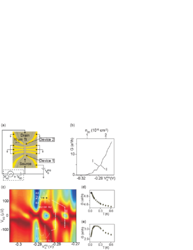
Devices were fabricated from high mobility Si--doped GaAs/Al0.33Ga0.67As heterostructures. The 2DEG is formed 300 nm below the surface, and the spacer layer between dopants and the 2DEG is 80 nm. Si doping density of cm-2 results in as-grown electron density cm-2 with low temperature mobilities cm2/V-s. By selective wet-etching a 8 m wide mesa is created. One thermally deposited 2 m long non-magnetic Ti/Au gate on the mesa is used to electrostatically vary cm-2 in the active m2 region. Fig. 1(a) shows an optical microscope image of a typical device with electric setup.
The devices were characterized in dilution refrigerators with base temperatures down to mK. Combined AC+DC two-probe measurements with ac excitation voltage is used for non-equilibrium transport spectroscopy. In fig. 1(b) we show a typical linear conductance , and for 30 mK at zero magnetic field. At temperatures mK, shows characteristic features of type-I, and type-II ZBA. For most devices, the structures are strongest in the electron density range cm-2, see fig. 1(b), and often visible up to . In non-equilibrium transport spectroscopy d/d consists of a repetitive sequence of two-types of resonances as is increased, see fig. 1(c). The single-peaked type-I ZBA splits intermittently to form a gap at , resulting in type-II ZBA. The insets (white) show the non-equilibrium traces of type-I ZBA, and type-II ZBA at the indicated in fig. 1(b).
Type-I ZBA decrease monotonically with increasing T, see fig. 1(d), and with increasing parallel magnetic field B [9]. In non-equilibrium transport spectroscopy type-I ZBA split with [13, 9]. Type-II ZBA show a non-monotonicity at the scale of over both T (see fig. 1(e)), and B, which is characteristic for interacting spins [10, 13, 9]. Type-I ZBA can then be understood as a spin lattice with . While the existence of mutually interacting localized spins in high-mobility mesoscopic heterostructures can account for such behavior, the question of spatial arrangement of the spins needs to be addressed independently with magnetoconductance measurements.
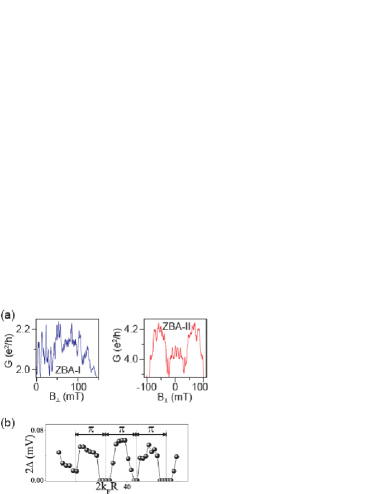
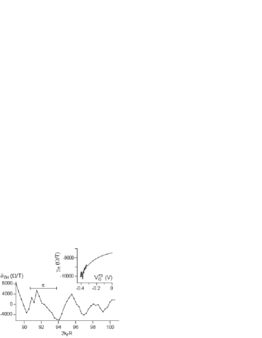
In two-dimensional spin lattice models, with localized spins arising from fluctuations in the conduction band, both Aharonov-Bohm like oscillations, as well as commensurability effects are expected [13]. Sites of localizes spins act as scattering centers, or as antidot, for conduction electrons, leading to back-scattering and interference effects when the phase coherence length of electrons exceeds . At low , a random spatial distribution of the scatterers or antidots gives rise to weak localization phenomena. The magnetoconductance then shows universal aperiodic fluctuations. However, for a quasi-regular antidot array, transport can be modeled through multiple, connected Aharonov-Bohm rings encircling a discrete number of impurities. Aharonov-Bohm like oscillations with periodicity , where is the radius of a stable ring [17, 18], appear. The oscillations can be assigned to the respective orbits via Fourier Transform, and the lowest possible orbit gives an estimate for [13]. Fig. 2(a) shows typical oscillations in the magnetoconductance for a type-I, and a type-II ZBA. We cross-checked the quasi regular distribution of the localized spins at higher from commensurability effects of classical electron trajectories in a 2D array of point scatterers at finite [19, 13]. Please note, that the magnetoconductance oscillations appear only over a range of , where ZBA is observed.
Associating each antidot to one (or more) localized spin then realizes a spin array embedded in the sea of conduction electrons [13]. These spins can interact via the conduction electrons by RKKY mechanism, and are then expected to have a characteristic periodicity of in . As , we can confirm this by plotting in fig. 2(b) . The clear periodicity of is recognized as the for RKKY typical -oscillations, establishing the existence of an interacting spin lattice in high mobility heterostructures [13].
3 Zero field Hall coefficient
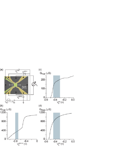
While non-equilibrium transport spectroscopy provides an indirect evidence of localized spins in high-mobility heterostructures, a convenient, and more direct, mean to probe the magnetic state of a two-dimensional spin lattice is the initial, or zero field, Hall coefficient. In case of magnetic order, the finite magnetization of the system adds an additional term to the Hall constant, resulting in the anomalous Hall effect (AHE) [20]. The Hall resistance is then , with being magnetic field, M being magnetization, in two dimensions, and being the anomalous Hall constant. We have designed fully tunable Hall devices, and show in fig. 3(a) an optical image with electrical setup. The 2DEG is laterally confined by two pairs of nonmagnetic Ti/Au sidegates with voltages V and V between -0.7 V and -0.8 V, which ensures defined QPCs, combined with low resistance Hall probes. Fig. 3(b) shows typical for the QPCs. The voltages V and V are adjusted at the beginning of the measurement, and kept constant during the whole experiment. The resulting 4-5 m wide electrostatically defined mesa is patterned with a full Ti/Au gate of dimensions m2 or m2 in between the two side gates. Voltage on the full gate V is applied to vary and thus create the active part of the device, with n cm-2. In fig. 3(c) we show for -0.8 V at the QPCs, and the range in which is operated in gray, which is chosen to ensure G for all V used.
With V and V both set at V, the conductance in the longitudinal direction was maintained at for all when the device was in operation for the Hall measurements. Please note that n2D and are higher in this experiment than in earlier ones to ensure free paths both in longitudinal, as well as in Hall direction. The electron density is determined at high n2D in the range of 50 mT, where no fluctuations are visible, and both low, and high T result in the same electron density (see inset of fig. 5). Lower electron densities were determined by extrapolating the dependence of on at the large regime via standard capacitance model.
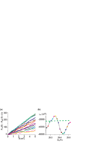
The samples are measured in a dilution refrigerator at base electron temperature 75 mK. Two probe low frequency ( 13 Hz) transport measurement with AC voltage V , and source-drain bias VSD is carried out such that current flows in the main direction through the active part only. Perpendicular magnetic field B⊥ is applied to measure the initial Hall coefficient , taken from the slope of the asymmetric Hall resistance R, with being the current, and being the Hall voltage on the QPCs, over the initial 2-5 mT. The asymmetric Hall resistance is taken only, to cancel out misalignment of Hall probes, and other field symmetric artifacts [21]. In fig. 4(a) we show the asymmetric component of the Hall resistance up to 5 mT, with different colors belonging to different electron densities. Via Aharonov-Bohm-type oscillations (Fig. 2) we find the interspin distance R m in these devices. The slope of the Hall resistance gives the Hall coefficient, which we show for the respective electron densities in fig. 4(b). The dashed green line indicates the unperturbed value of , and shows a strong deviation from its high temperature value.
The Hall coefficient deviates both positively and negatively with respect to the unperturbed value . The positive contribution to is unexpected, and has the wrong sign for a magnetic contribution via the anomalous Hall effect. The negative deviation is expected for a magnetic interaction in a spin lattice. To investigate that further, we have considered a larger range of densities, and show in fig. 5 the range . For clarity, only the deviation is plotted. For a given period in , the deviation again is either positive or negative, and overall, the magnitude of this deviation decreases when the carrier density is increased. This can be due to the screening of localized spins, which increases with increasing electron density, and reduces the visibility of the localized spins. has a rough periodicity of = , indicating a common origin of these fluctuations and the ZBA in nonequilibrium transport.
Please note that clean periodicity of fluctuations in requires the whole device area to be in the same phase. Since the formation of the intrinsic spin lattices does not yield perfect regularity in interspin distance over the whole m2 or m2 in 100% of our devices, we do also observe random fluctuations, and show in fig. 6c) also a bad device.
3.1 Stability of fluctuations
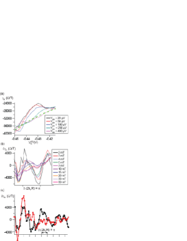
In fig. 6(a) we show a typical fluctuation of for various source drain biases. For all other experiments was kept constant. The fluctuation vanishes with increasing , and is back to its unperturbed value (shown as dashed green line) at about .
In fig. 6(b) we show the deviation of , calculated from slope of the asymmetric Hall resistance in various B field ranges, from . The lowest field ranges show strongest fluctuations, and increasing field range decreases the intensity of the fluctuations. Since the interspin interaction itself couples to very small transverse fields [22], the fluctuations are only meaningful when the slope is computed over smallest field ranges, i.e., leading to the zero field Hall coefficient. Since very low field ranges do also increase the error in the data, we use 2-5 mT range for all data. We find that the highest field range 50 mT is mostly similar to the unperturbed Hall coefficient evaluated from the high density range and capacitance model.
By increasing the temperature the fluctuations in vanish (not shown), confirming the oscillations in Hall coefficient to be a low effect.
As mentioned before, disorder appears to be a crucial aspect of the fluctuations in . We therefore show in fig. 6(c) an example of a bad sample with strong disorder, and mostly irregular fluctuations in . While no periodicity over the whole range can be seen, most adjacent fluctuations are still showing a rough -periodicity, although not as clear as the less disordered devices. While the overall magnitude of fluctuations is increasing with lower densities, we find that the clean regularity of the fluctuations is decreasing with decreasing , where more random scattering appears. To avoid this we now record data at higher electron densities only, and find much cleaner -periodic fluctuations, with only very little disorder.
The role of the confinement voltage is also shown in fig. 6(c). The red trace is shown for a confinement voltage of -0.7 V, and the black one for -0.8 V. The fluctuations in change the overall appearance with change in gate voltage, but not the characteristics. This is a very important point to note, as the state of the device should only weakly depend on the confinement voltage. When comparing the red and black traces, then minima, and maxima of are untouched by the confinement voltage.
An important question to be addressed is the origin of the localized spins. While a model with localized spins arising from doping was suggested and analysed earlier [13], other origins can not be excluded yet. The interface between GaAs/AlGaAs could potentially induce potential fluctuations in the 2DEG. In our system the lattice constants are m and m, resulting in a lattice mismatch of , and an average defect distance of m. This is close to the length scale we observe, but the defects are expected to be in stripes, not in puddles, as observed in our measurements. A purely electrostatic origin for the spin lattice might also cause such ZBA, but it is difficult to imagine how the large length scale arises. Currently, experiments are carried out that will enable a more detailed insight into the origin of the localized spins [23].
4 Summary
We report existence of an intrinsic spin lattice in high mobility GaAs/AlGaAs heterostructures. The localized spins interact indirectly via RKKY interaction, and the magnetic state of the lattice can be tuned with a simple non-magnetic surface gate. The interspin distance can be evaluated with Aharonov-Bohm like interference at low temperatures, and commensurability effects at higher temperatures. To probe the magnetic state directly, a Hall geometry is introduced, and existence of fluctuations in the Hall coefficient shown. The fluctuations are periodic in , and deviate positively and negatively from the non-interacting value .
5 Acknowledgment
This project was supported by EPSRC. CS acknowledges the support of Cambridge European Trust, EPSRC, and Gottlieb Daimler and Karl Benz Foundation.
References
- [1] J. H. Smet, R. A. Deutschmann, F. Ertl, W. Wegscheider, G. Abstreiter, and K. von Klitzing, Nature 415, 281 (2002).
- [2] V. Madhavan, W. Chen, T. Jamneala, M. F. Crommie, and N. S. Wingreen, Science 280, 567 (1998).
- [3] D. Goldhaber-Gordon, H. Shtrikman, D. Mahalu, D. Abusch-Magder, U. Meirav, and M. A. Kastner, Nature 391, 156 (1998).
- [4] S. M. Cronenwett, T. H. Oosterkamp, and L. P. Kouwenhoven, Science 281, 540 (1998).
- [5] C. Jayaprakash, H.R. Krishnamurthy, and J.W. Wilkins, Phys. Rev. Lett. 47, 737 (1981).
- [6] Affleck, I. & Ludwig, A. W. W. Exact critical theory of the two-impurity Kondo model. Phys. Rev. Lett. 68, 1046 (1992).
- [7] N. J. Craig, J. M. Taylor, E. A. Lester, C. M. Marcus, M. P. Hanson, and A. C. Gossard, Science 304, 565 (2004).
- [8] L. Kouwenhoven and L. Glazman, Physics World January (2001).
- [9] A. Ghosh, M. H. Wright, C. Siegert, M. Pepper, I. Farrer, C. J. B. Ford, and D. A. Ritchie, Phys. Rev. Lett. 95, 066603 (2005).
- [10] H. B. Heersche, Z. de Groot, J. A. Folk, L. P. Kouwenhoven, H. S. J. van der Zant, A. A. Houck, J. Labaziewicz, and I. L. Chuang, Phys. Rev. Lett. 96, 017205 (2006).
- [11] W. G. van der Wiel, S. De Franceschi, J. M. Elzerman, S. Tarucha, L. P. Kouwenhoven, J. Motohisa, F. Nakajima, and T. Fukui, Phys. Rev. Lett. 88, 126803 (2002).
- [12] A. Ghosh, C. J. B. Ford, M. Pepper, H. E. Beere, and D. A. Ritchie, Phys. Rev. Lett. 92, 116601 (2004).
- [13] C. Siegert, A. Ghosh, M. Pepper, I. Farrer, and D. A. Ritchie, Nature Physics 3, 315 (2007).
- [14] A.N. Pasupathy, R.C. Bialczak, J. Martinek, J.E. Grose, L.A.K. Donev, P.L. McEuen, and D.C. Ralph, Science 306, 86 (2004).
- [15] J. Nygard, D.H. Cobden, and P.E. Lindelof, Nature 408, 342 (2000).
- [16] M. T. Bal-Monod, Phys. Rev. B 36, 8835 (1987).
- [17] R. Schuster, K. Ensslin, D. Wharam, S. K hn, and J.P. Kotthaus, Phys. Rev. B 49, 8510 (1994).
- [18] Weiss, D. et al. Phys. Rev. Lett. 70, 4118 (1993).
- [19] Weiss, D. et al. Phys. Rev. Lett. 66, 2790 (1991).
- [20] H. Toyosaki, T. Fukumura, Y. Yamada, K. Nakajima, T. Chikyow, T. Hasegawa, H. Koinuma, and M. Kawasaki, Nat Mater 3, 221 (2004).
- [21] W. Teizer, F. Hellman, and R. C. Dynes, Phys. Rev. B 67, 121102 (2003).
- [22] C. Siegert, A. Ghosh, M. Pepper, I. Farrer, D. A. Ritchie, D. Anderson, G. A. C. Jones, submitted to PRL.
- [23] S. Sarkozy et al., to be published