Electric field gradient induced effects in GaAs/AlGaAs modulation-doped structures and high frequency sensing
Abstract
Electric field gradient effects induced by an asymmetrically in-plane shaped GaAs/AlGaAs modulation-doped structures of various design are investigated within 4–300 K temperature range. It is demonstrated that current–voltage characteristics of such structures at low, 4–80 K, temperatures exhibit well-pronounced asymmetry arising due to a presence of two different gradients of the electric field in a two dimensional electron gas. This phenomenon is caused by both, different accumulation of two-dimensional electrons due to asymmetrical shape of the structure and nonlocality in the electron drift velocity. Experiments are illustrated by a phenomenological model and Monte Carlo simulation. Possible applications of the effect to detect electromagnetic radiation of GHz and THz frequencies are discussed as well.
pacs:
71.55.Eq, 73.61.-r, 73.23.AdI Introduction
As it is known, in modulation-doped (or selectively-doped) structures free electrons, spatially separated from ionized donors, are confined to a narrow potential well forming the so-called two-dimensional electron gas (2DEG)stormer1979 ; hiyamizu1983 . the axis, i. e. perpendicular to the 2DEG plane, the confinement potential has a triangular shape, and the spectrum of the 2DEG is composed of a sequence of quantum subbands.ando1982 The shape of the confining potential has influence only to the carrier transitions between different subbands; meanwhile for excitations within each subband – so-called intraband excitations – this effect is very small. to the axis, i. e. in the 2DEG, or plane, the carriers display very high electron mobilities exceeding values of 2/(Vs) at liquid nitrogen and 1/(Vs) at liquid helium temperatures.heiblum1984 This fundamental property of these structures allowed to invent HEMTs – high electron mobility transistors.mimura1980
The carrier transport in 2DEG layers at low electric fields is described by the Ohm’s law together with the Einstein relation for the diffusion coefficient, i.e.
| (1) |
where is drift velocity, stands for electron mobility, is the electric field and is the free carrier concentration; is the electron charge, and denote Boltzmann constant and lattice temperature, respectively. This so-called ”drift-diffusion equation” describes the quasi-classical situation when the quantization of the electronic states-induced effects are not important. On the other hand, it does not take into account the hot-electrons phenomena when the applied in-plane electric field is strong enough to heat the electrons up to the energy exceeding their equilibrium value.price1988
The electric field in modelling, as a rule, is assumed to be uniform. Although this assumption is very convienent for calculations, however, in many cases, in order to obtain the real picture of physical processes, it is necessary to include spatial variation of the carrier concentration or/and the electric field along the channel. In particular, when it becomes comparable with the range of a mean free path. Under these circumtances, effects such as velocity overshoot begin to predominate defining thus the performance of the device. Such an approach is very important, for instance, in understanding the behavior of devices containing asymmetric channel profile produced by a relevant doping. More specifically, in a quarter-micron -type silicon metal-oxide semiconductor field effect transistors (MOSFET) with asymmetric channel profile, formed by the tilt-angle ion-implantation after gate electron formation, allows one to achieve high current drivability and hot-electron reliability.buti1991 For example, in 0.1 m gate length asymmetric -MOSFET structures this technological innovation allows to attain higher electron velocity in comparison with conventional devices of such type.odanaka1997
In this article, we report on experimental and theoretical investigation of the electric field gradient-induced effects due to asymmetrically in-plane shaped GaAs/AlGaAs modulation-doped structures. We show that current–voltage characteristics of such structures at low, 4–80 K, temperatures exhibit pronounced asymmetry. The physics behind is attributed to a two-dimensional bigradient effect which is equivalent to the phenomenon observed earlier in a bulk asymmetricaly-shaped semiconductorsasmontas1975 ; stepas1975 . We demonstrate that depending on the values of the in-plane electric fields and their gradients, the effect can reveal itself as a result of different distribution of accumulating two-dimensional electrons due to the asymmetrical shape of the structure, and/or the exhibition of nonlocal drift velocity which becomes pronounced in a different manner due to the presence of two different gradients of the in-plane electric field.
The paper is organized as follows. In Sec. II we present the design of the GaAs/AlGaAs modulation-doped structures, their electrical parameters and geometry features; we also describe briefly used measurement techniques. Section III reports on experimental results obtained in GaAs/AlGaAs modulation-doped structures of various designs and at different lattice temperatures. Section IV is devoted to theoretical models and illustrates the concept of the electric field gradients-induced phenomenon – the bigradient effect with special emphasis on manifestation of the electron drift velocity. In Sec. V possible applications of the effect for the sensing of electromagnetic radiation within GHz–THz frequencies are disccused, while in Sec. VI features of three-dimensional vs. two-dimentional effect are compared. Finally, conclusions are given in Sec. VII.
II Samples and measurement techniques
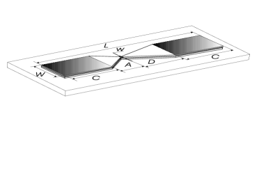
Two types of modulation-doped structures of GaAs/Al0.25Ga0.75As (structure 2DEG-A) and GaAs/Al0.3Ga0.7As (structure 2DEG-B) were grown by molecular beam epitaxy technique. Their design parameters are given in the caption of Fig. 1.
Electron sheet density, , and low-field mobility, , at different, 300 K, 77 K and 4.2 K, temperatures for structure 2DEG-A are the following: 5.5 and /(Vs), 1.9 and /(Vs), 1.9 and 2/(Vs), respectively; while for structure 2DEG-B: 5.6 and /(Vs), 4.3 and /(Vs), 4.3 and 1/(Vs), respectively.
The wafers were then processed into asymmetrically-shaped samples of different geometry which was changed varying the width of the neck. We have used the optical lithography for the samples with = 12 m. The meza with height, , of 2 m in these samples was fabricated by wet etching. In order to fabricate samples with a narrower neck, respectively 5 m, 2 m, and 1 m width, we have employed electron-beam lithography and shallow wet etching; the meza height in this case was 300 nm. The Ohmic contacts were produced by a rapid annealing procedure of evaporated Au/Ge/Ni compound.
The wired samples were then mounted into a two-stage closed-cycle helium cryostat, and characteristics were measured within 4–300 K temperature range. In microwave experiments performed at 10 GHz frequency, we have used magnetrons delivering pulses of 1.5–5 s duration with the repetition rate of 35–40 Hz; the samples were then placed into rectangular waveguides, and the microwave radiation-induced voltage arising over the ends of the sample was measured by an oscilloscope; the experiments were performed at room and liquid nitrogen temperatures. In the terahertz (THz) range, 0.584–2.52 THz, the source of THz radiation was an optically-pumped molecular laser operating in the continuous wave regime; the illumination into the sample, located in the closed-cycle helium cryostat behind the THz transparent high-pressure polythene window, was focused by spherical mirrors. As in the microwave case, the external radiation-induced voltage arising over the ends of the sample was recorded by lock-in amplifier at a chopper frequency of 187 Hz.
III Experimental Results
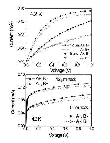
Figure 2 shows the experimental results of characteristics measured in structure 2DEG-A in the samples with different neck widths recorded at liquid helium temperature. (The experimental data of the structure 2DEG-B are equivalent and therefore are not presented here).
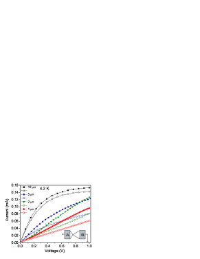
As one can see, the salient feature of all the measured characteristics is an asymmetry becoming well-procounced above 0.1 V. Moreover, the character of the characteristics strongly distingtive to the reduction of the neck width: For the sample with neck width of 12 m two parts in the curve can be distinguished – the initial rising part (below 0.3 V) which bends with voltage and above 0.7 V transits to the second, saturated one. With the decrease of the width the saturated part transforms to a boosting region with highly expressed asymmetry. A complex behaviour is observed in the 5 m width sample: careful look can resolve initial rising part below 0.15 V, rudiments of saturated part within 0.15–0.6 V and already emerging boosting region above 0.6 V with spread influence on all the curve.
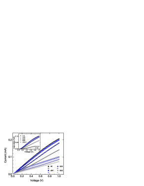
It should be pointed out that the asymmetry is strongly sensitive to the temperature variation. This is illustrated by the experimental data for 2 m neck sample given in Fig. 3. It is seen that at low temperatures the asymmetry is rather large – if the coefficient of asymmetry of the characteristics is defined as – at liquid helium temperature under 0.8 V it is 0.506, at 80 K its value is about 0.369, meanwhile at room temperature the asymmetry is nearly invisible. To resolve the effect, the experimental data should be multiplied by a factor of one hundred.
IV Theoretical approach and physics behind
IV.1 Electric-field gradient-induced effects: carrier accumulation
To understand the physics behind the observed phenomenon, we have followed the same ideology as in the bulk case of asymmetrically-shaped structures: We explore an asymmetrically shaped two-dimensional structure by a solving a coupled system of one-dimensional Poisson and current-flow equations neglecting quantum effectsasmontas1975 ; stepas1975 :
| (2) | |||
| (3) |
where denotes the position along the symmetry axis of the asymmetrically-shaped sample, is the cross-section area of the sample, is the electron concentration, is the donor concentration (used here as a free fit parameter), denotes the electric field strength, is the dielectric constant of the sample, denotes the diffusion coefficient, and is the electron mobility. The diffusion coefficient may be set to a constant value as its dependence on the electric field has no appreciable influence on the results. As it is known, mobility changes with the electric field:shah1984 , where , and is the cut-off velocity equal to cm/s.
For a given value of the current , one can employ an iterative scheme to solve self-consistently the system and calculate the voltage.
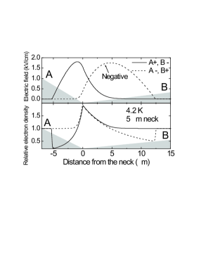
Results of the electric field and relative carrier density calculations are given in Fig. 4. The model calculations do give two different gradients of the electric field induced by the asymmetrical shape of the structure depicted in Fig. 1. One must note further that the distribution depends on the current direction, and this difference is appreciable only within several microns from the neck: The electric field peaks are sharper in the case of the reverse current, when the A-contact of the sample is under a positive bias.
Hence, the in-plane geometrical asymmetry induces two different gradients of the electric field in the sample. As a consequence, different spatial accumulation of two-dimensional electrons in the vicinity of the neck can be a reason for asymmetric curves. This prediction is confirmed by the theoretically calculated characteristics and their comparison with the experimental data presented in Fig. 5. As one can see, the measured and calculated curves in 12 m neck width samples behave similarly: in low electric fields, where Ohm’s law is still valid, the current values are the same and do not depend on the polarity of the applied voltage. However, with the increase of voltage – when sample is tuned to a strong field regime – the electrons become hot, they accumulate differently in the vicinity of the neck due the asymmetrical shape of the structure. As a result, the asymmetry in the characteristics is observed. Since this phenomenon relies on hot-carriers, it is reasonable that is temperature-sensitive: the decrease of lattice temperature will make the effect much more pronounced since the carrier heating at low temperatures is stronger. This is clearly seen in Fig. 3: the difference between the forward and the reverse-bias curves, for instance, at room temperatureroom is approximately by three orders of magnitude smaller than that at 4.2 K temperature in the given voltage range. The temperature effect is also confirmed by theoretical calculations (data are not given here).
Therefore, the presence of two different electric field gradients in the hot two dimensional electron regime, allows one to explain the asymmetry of characteristics at low temperatures. The phenomenon can be called thus the two-dimensional bigradient effect.
It is reasonable that the reduction of the neck should cause stronger asymmetry in curves. Experimentally it is clearly illustrated in Fig. 2. However, if one compares the behavior of the curves, for instance, for the 5 m neck sample with a corresponding theoretical estimates (Fig. 5), evident differences can be indentified:
the theory does not follow the experiment anymore neither in curve shape nor in asymmetry value. Therefore, in order to understand the origin of the behavior, a more complete theoretical model must be applied.
IV.2 Electric-field gradient-induced effects: Influence of nonlocality in drift velocity
Althought the equation (1) is the backbone of electronic device simulations, in the current situation one needs to be extended taking into account the electric field gradient-induced term.price1988 The electron average velocity can be then expressed using the extended/augmented drift-diffusion modelsonoda1996
| (4) |
where is the drift velocity in a homogeneous electric field, denotes diffusion coefficient, depics the length coefficient. The latter parameter is in the order of electron mean free path and determines the severity of the velocity overshoot effect which is pronounced when the variation range of the electric field is equal to or shorter than . Also, it is worth noting that in the given equation we have assumed that nonlocality in diffusion coefficient is negligible and has no observable influence on the effect.
A point of departure for analyzis is an estimate of a mean free path () of two dimensional electrons at liquid helium temperatures. As electron mobility in the studied structures is of about 1/(Vs), this results to the value of
| (5) |
where =0.068, the latter is the free electron mass. Meanings of other symbols are the same as in previous formulae.
The second step in considering the data is an estimate of the distribution of the electric field in the vicinity of the neck. Voltage value of 0.25 V was chosen as a reference point, since experimentally observed asymmetry of the characteristic starts to be strongly expressed. Theoretical calculations using the set of equations (2 – 3) are given in Fig. 6. As one can see, the shape of the
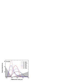
electric field distribution strongly varies with the reduction of the neck width: it becomes sharper and the asymmetry becomes more pronounced. Futhermore, distribution of the electric field is squeezed to the narrower range. If for 12 m width sample the electric field extends over 1.7 m, in the 5 m and 2 m necks it is of about 1.2 m and 0.9 m, respectively. One can assume therefore that in 5 m neck samples the nonlocality can start to predominate since the change of the electric field along the structure is comparable with the electron balistic length.
Calculations illustrating the effect of nonlocality in electron drift velocity on characteristics are given
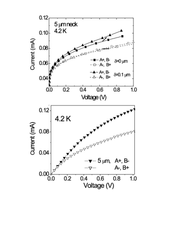
in Fig. 7. One can see that increase of has obvious effect in 5 m neck sample – even small increase in length coefficient (in the range of 0.1–0.2 m) stimulates the raise in the asymmetry. It is evident that calculations for the 5 m are very similar to the given experimental results. It is deserve to remark that in 12 m neck samples such the influence is not observed (these theoretical data are omitted here).
The inherent feature of the nonlocal effects is a manifestation of the velocity overshoot. To evidence the latter we have performed the Monte Carlo calculations of the drift velocity in a ”frozen” electric field taken from a solution of the coupled set of Poisson and current-flow equations (Eq. 2-3) as described previously. We have simulated the drift of Monte Carlo particles along the x-direction in the given electric field distribution assuming that the particles enter the modelling region having the Boltzmann distribution at the lattice temperature. The standard three-valley GaAs model is applied in the simulationhess-1984 with an impurity scattering rate corresponding to a donor concentration. Figure 8 presents simulated electron velocity profiles in forward and reverse directions at the electric field profiles for 5 m neck samples. For the sake of evidence, the electric field profiles taken from Fig. 6 are given, too. As one can see, the velocity overshoot/undershoot and strong nonlocality effects are clearly visible.
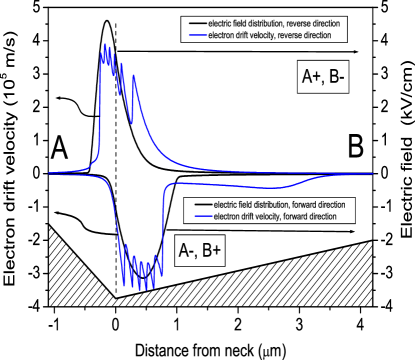
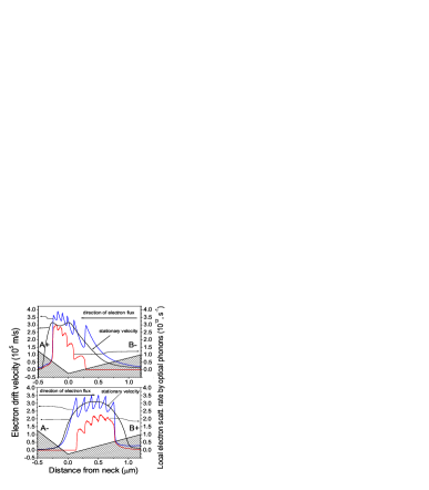
The sharp peaks at the top of the velocity profiles are related to the locality in optical phonon emission rate . Note that the velocity profile is asymmetric due to the presence of the different electric field gradients and exhibits nearly constant value in the forward direction ranging from 0.75 up to 3 m. The Monte Carlo simulation for electric field profiles from Fig. 8 gives the coefficient of current asymmetry of 0.48. The factor strongly depends on impurity scattering rate: it decreases as the scatering rate increases. The simulation with donor concentrations 2, 1, and 5 gives the coefficient values of 0.62, 0.48, and 0.25, respectively.
To get close-up view in the physics behind, we have depicted the velocity and profiles in both, forward and reverse, directions (Fig. 9). Also, stationary velocity is added to illustrate the overshoot/undershoot areas. It is obvious that the electron velocity minima coincide with the maxima forming thus ”comb” in electron distribution. The effect is equivalent to the the free-carrier grating formation phenomenon caused by locality of optical phonon emission as already demonstrated in InN structures.viktor-2004
V possible applications of the effect
Since the two-dimensional bigradient effect induces asymmetry in -characteristics, it is reasonable to consider its possible applications in detection of the high-frequency electromagnetic radiation. To test this idea, we have placed samples in a microwave field of 10 GHz frequency and recorded microwave-induced voltage arising over the ends of the sample. The results for two samples of different neck width recorded at room and liquid nitrogen temperatures are displayed in Fig. 10(a).
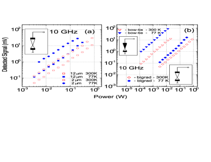
One can see that with the increase of incident power the signal increases linearly in all the range of studied power. Thus, due to the asymmetry in curves caused by the two-dimensional bigradient effect the microwave radiation can be detected THz-detect . However, as estimates show, the sensitivity at room temperature is rather low. For instance, it is only about 12 mV/W and 40 mV/W for the samples with neck width of 12 m and 2 m, respectively. Since the effect is related to the electron heating, the decease in temperature should induce the increase in the detected signal. The temperature effect, however, is not as large as might be expected from hot-electron physics where change of the signal is proportional to the carrier mobility. As one can see, at 77 K, the detected voltage increases reaching the values of 40 mV/W (12 m neck sample) and 150 mV/W (2 m neck sample). In fact, the rise in only by a factor of about 4, while the mobility increases about 14 times. We associate the outcome with a presence of ballistic electrons which cross the effective length of the samples without scattering.shur2002 It is evident that for implementation of the effect into practical devices, such a sensitivity values are not sufficient. Following the ideology of the bigradient effect, one needs to produce much higher non-uniformity of the electric field in the sample’s neck vicinity. This can be achieved easily by metallizing one of the asymmetric parts of the structure. This is evidenced by calculations of the distribution of the electric field given in Fig. 11.
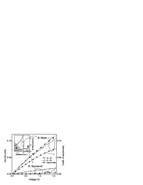
It is seen that the non-uniformity of the electric field with one part of the sample metallized is much stronger than in the conventional asymmetrically-shaped structure. It is therefore reasonable to expect significantly higher values of the sensitivity. The experimental illustration is given in Fig. 10(b) where the bigradient structures are compared with the so-called 2DEG bow-ties diodesbow-ties – structures where one of the parts of the sample is covered by metal. One can see that these devices are nearly in two orders of magnitude more sensitive compared to the structures of bigradient-design.
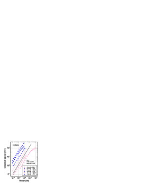
Of particular interest for the direct applications are the values of the voltage sensitivity at room temperature. In order to increase the sensitivity of the diode, we have chosen the design 2DEG-B (due to the higher value of the sensitivity at room temperature) and reduced the size of the apex down to 2 m keeping the other geometrical dimensions the same (Fig. 12). As one can see, in this case the detected signals are significantly larger than for the 12 m neck diodes at 300 K, and the sensitivity amounts to 2.5 V/W, which is nearly one order of magnitude higher compared to the diodes of 12 m neck width, where it is about 0.32 V/W. The decrease in temperature down to 77 K allows one to increase the sensitivity up to nearly 40 V/W, i.e. close to a factor of 14.5 which corresponds to the change of 2DEG mobility. The latter effect – via thickness of spacer – is also nicely expressed in Fig. 12 were the detected signal in both devices, fabricated from 2DEG-A- and 2DEG-B-type structures is compared.
Additionally, it deserves mentioning that the further decrease of the neck size down to 1 m – 800 nm, gives, however, no increase in the sensitivity (the data are not presented here). We attribute it to weaker coupling of the microwave field into the structure with the reduction of the neck width.
As to dynamical range, the devices can be used to detect rather different power levels. As already indicated above, the bigradient modulation-doped structures at 300 K in microwaves exhibit sensitivity of about 12 mV/W and 40 mV/W for the samples with neck width of 12 m and 2 m, respectively, however, the sensing range is below 1 W in a pulse mode, i.e. the resistance to overloading is small. Bulk silicon-based 12 m neck width structures are also not sensitive – only about 0.1 V/W – but they can withstand up to 10 kW maximum applied power at room temprature without any negative outcome.algis1999 Asymmetrically-shaped bulk GaAs structures containing -junction were found to be suitable for broadband sensing within GHz–THz frequencies at 300 K.algis-gintaras-jap2003
Finally, it is worth to remark on the operation of the bigradient structures within the THz range. One can note that at 300 K the sensitivity at 0.763 THz in the sample with neck width of 12 m it is about 13 mV/W, i.e. close to the value in 10 GHz range. Narrowing the neck width down to 2 m, the sensitivity at 0.763 THz can increase up to 17 mV/W. Within frequencies 1.41 THz, 1.63 THz and 2.52 THz the detection observed is rather poor. We explain it by a weak coupling of the incident THz field into the structure. At helium temperatures, the sensitivity reaches the value of 60 mV/W at 0.763 THz for the 12 m neck width sample.estimate
VI Two-dimensional vs. bulk bigradient effect
The effect was originally discovered by measuring characteristics in bulk semiconductors, -Ge and -Si, at room and liquid nitrogen temperatures.asmontas1975 ; stepas1975 In what follows we compare the two-dimensional bigradient effect observed in asymmetrically in-plane shaped GaAs/AlGaAs modulation-doped structures with its bulk equivalent desribed in details.asmontas1985
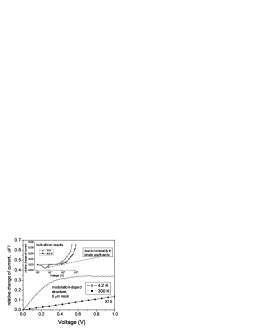
The inherent fearure of both – the two-dimentional and bulk – effects is asymmetry in characteristics. Different material parameters and geometrical dimensions of the samples determine rather distinctive voltage scale and temperature conditions for experimental observation. The effect of the dimensionallity we associate with unusual manifestation of the nonlocality in drift velocity. Figure 13 presents a change of the relative current in 5 m neck size sample at 4.2 K and 300 K. For comparison of the features, inset shows equivalent bulk data measured in -type silicon according to Ref. 19.
It is seen that in the bulk semiconductor the nonlocality is associated with the sign change in the asymmetry clearly observed within 1-10 V voltage scale at 77 K (see inset). In contrast, in modulation-doped structure, no such peculiarity is observed. It is worth noting, however, that above 0.3 V the change of the relative current is nearly independent of voltage – as was indicated earlier (Fig. 7, above 0.25 V range, where asymmetry of characteristics strongly increases) – we attribute it to the apperance of the nonlocal drift velocity.
VII Conclusions
Asymmetrically in-plane shaped GaAs/AlGaAs modulation-doped structures of various design are studied within 4–300 K temperature range. We have shown that current–voltage characteristics of such structures at low, 4–80 K, temperatures exhibits pronounced asymmetry which we explain by a two-dimensional bigradient effect. This phenomenon can be decomposed into two constituents – carrier accumulation and nonlocality in the electron drift velocity – each of which manifests itself depending on the values of the in-plane electric fields and their gradients. Varying these parameters via change of the sample neck we have inferred that the effect is induced by different accumulation of two-dimensional electrons due to asymmetrical shape of the structure when the neck size down is 12 m; in 5 m neck size structures in electric fields close to 3 kV/cm, the nonlocality of the electron drift velocity becomes predominating causing thus further increase of the asymmetry in curves. The theoretical models suggested conform well with the obtained experimental results. Monte Carlo simulation has shown strong nonlocal effects in the electron drift velocity and presence of overshoot/undershoot regions depending on the electric field and its gradient values. The features of the two-dimensional bigradient effect and its bulk equivalent are compared and possible applications of this phenomenon to detect electromagnetic radiation of GHz and THz frequencies are discussed as well.
Acknowledgements.
We sincerely grateful to Vincas Tamošiūnas, Jurek Lusakowski and Kirill Alekseev for valuable and comprehensive discussions; our highest possible appreciations go to Adolfas Dargys for his illuminating remarks and delicate suggestions in the manuscript preparation, and Antanas Reklaitis for useful notes on simulation matters. The work was supported, in part, by the NATO SfP project 978030 ”Broadband detectors”. The research at the Semiconductor Physics Institute at Vilnius was performed under the topic ”Study of semiconductor nanostructures for terahertz technologies” (No. 144.3).References
- (1) Corresponding author; electronic mail address: valusis@pfi.lt
- (2) Current address: Device Technology - Technology Development, Chartered Semiconductor Manufacturing Ltd., 60 Woodlands, Industrial Park D, Street 2, Singapore 738406
- (3) H. L. Stormer, R. Dingle, A. C. Gossard, W. Wiegmann, and M. D. Sturge, Solid State Commun. 29, 705 (1979).
- (4) S. Hiyamizu, J. Saito, K. Nanbu, and T. Ishikawa , Jpn. J. Appl. Phys. 22, L609 (1983).
- (5) T. Ando, A. B. Fowler, and F. Stern, Rev. Mod. Phys. 54, 437 (1982).
- (6) M. Heiblum, E. E. Mendez, and F. Stern, Appl. Phys. Lett. 44, 1064 (1984).
- (7) T. Mimura, S. Hiyamizu, T. Fujii, and K. Nambu, Jpn. J. Appl. Phys. 19, L225 (1980).
- (8) P. J. Price, J. Appl.Phys. 63, 4718 (1988).
- (9) T. N. Buti, S. Ogura, N. Rovedo, and K. Tobimatsu, IEEE Trans. Electron Devices, 38, 1757 (1991).
- (10) S. Odanaka and A. Hiroki, IEEE Trans. Electron Devices, 44, 595 (1997).
- (11) S. Ašmontas, K. Požela, and K. Repšas, Lithuanian J. Phys. 15, 249 (1975).
- (12) S. Ašmontas, Phys. Stat. Sol.(a) 31, 409 (1975).
- (13) J. Shah, A. Pinczuk, H. L. Störmer, A. C. Gossard, and W. Wiegmann, Appl. Phys. Lett. 44, 322 (1984).
- (14) It is worth noting that the different-bias curves at room temperature separate noticeably only at voltages above 10 V.
- (15) K. Sonoda, K. Kanno, K. Taniguchi, and C. Hamaguchi, Jpn. J. Appl. Phys. 35, L1398 (1996).
- (16) K. Brennan and K. Hess, Solid-State Electron. 27, 347 (1984).
- (17) V. Gružinskis, P. Shiktorov, E. Starikov, L. Reggiani, L. Varani, J. C. Vaissiere. Semicond. Sci. Technol. 19, S173 (2004).
- (18) D. Seliuta, E. Širmulis, V. Tamošiūnas, S. Ašmontas, A. Sužiedėlis, J. Gradauskas, G. Valušis, P. D. Steenson, W.-H. Chow, P. Harrison, A. Lisauskas, H. G. Roskos, and K. Köhler, Proc. 27th Intern. Conf. Physics on Semiconductors ICPS-27, Flagstaff, Arizona, USA, 26-30 July 2004; Editors: José Menédez and Chris G. Van de Walle, AIP Conference Proceedings, Vol. 772 (published June 2005; ISBN 0-7354-0257-4, Two Volume, Print; 1697 pages), P. 1204-1205.
- (19) M. S. Shur, IEEE Electron Device Lett. 23, 511 (2002). Here the concept of ”ballistic” – not a real mobility (as it is known, it relates to the collision dominated regime) – was introduced in order to point out that the effective electron mobility in a short channel can be much smaller than in the long one.
- (20) Concept of the 2DEG bow-ties diodes and their demonstration for microwave detection: A. Juozapavičius, L. Ardaravičius, A. Sužiedėlis, A. Kozič, J. Gradauskas, J. Kundrotas, D. Seliuta, E. Širmulis, S. Ašmontas, G. Valušis, H. G. Roskos, and K. Köhler, Semicond. Sci. Technol. 19, S436 (2004); for detection of THz/subTHz frequencies at room temperature: D. Seliuta, E. Širmulis, V. Tamošiūnas, S. Balakauskas, S. Ašmontas, A. Sužiedėlis, J. Gradauskas, G. Valušis, A. Lisauskas, H. G. Roskos, and K. Köhler, Electron. Lett. 40, 631 (2004).
- (21) S. Ašmontas, Electrogradient Phenomena in Semiconductors, Mokslas, Vilnius, 1984, p. 141–152 (in Russian).
- (22) S. Ašmontas, J. Gradauskas, A. Sužiedėlis, and G. Valušis, Physica Scripta T79, 330 (1999).
- (23) A. Sužiedėlis, S. Ašmontas, J. Gradauskas, G. Valušis, and H. G. Roskos, J. Appl. Phys. 93, 3034 (2003).
- (24) The sensitivity was estimated scaling the spatial profile of the THz beam, calculating power density and multiplying it by area of the structure. It was assumed that all the incident power is absorped by the sample.