ENGINEERING THE PHASE SPEED OF
SURFACE–PLASMON WAVE AT THE PLANAR INTERFACE OF A METAL
AND
A CHIRAL SCULPTURED THIN FILM
Akhlesh Lakhtakia1 and John A. Polo Jr2
1CATMAS — Computational & Theoretical Materials Sciences Group,
Department of Engineering Science and Mechanics,
Pennsylvania State University,
University Park, PA 16802, USA.
e–mail: akhlesh@psu.edu
fax: (814) 865 9974
2Department of Physics and Technology,
Edinboro University of Pennsylvania,
Edinboro, PA 16444, USA.
e–mail: polo@edinboro.edu
fax: (814) 732 2455
ABSTRACT The solution of a boundary–value problem formulated for a modified Kretschmann configuration shows that the phase speed of a surface–plasmon wave guided by the planar interface of a sufficiently thin metal film and a chiral sculptured thin film (STF) depends on the vapor incidence angle used while fabricating the chiral STF by physical vapor depoistion. Therefore, it may be possible to engineer the phase speed quite simply by selecting an appropriate value of the vapor deposition angle (in addition to the metal and the evaporant species).
Keywords: Kretschmann configuration, metal optics, sculptured thin film, structural handedness, surface plasmon
1. INTRODUCTION
The solution of a boundary–value problem formulated for a modified Kretschmann configuration has recently shown that a surface–plasmon wave can exist at the planar interface of a sufficiently thin metal film and a nondissipative structurally chiral medium, provided the exciting plane wave is –polarized [1]. Surface–plasmon waves in the visible and the near–infrared regimes are being exploited nowadays for sensing, imaging, and other applications [2, 3, 4, 5]. Structurally chiral mediums exist as chiral nematic and chiral smectic liquid crystals [6] as well as chiral sculptured thin films (STFs) [7].
In addition to their structural handedness (left or right) and their structural period along the axis of helicoidal nonhomogeneity, chiral nematic liquid crystals are characterized by two relative permittivity scalars: and . Chiral smectic liquid crystals and chiral sculptured thin films, however, are characterized by three relative permittivity scalars (, , and ) as well as a tilt angle . Our focus here is on chiral STFs, which are fabricated by physical vapor deposition [7].
The constitutive parameters of a chiral STF can be substantially engineered by controlling a few deposition variables. While a chiral STF is being grown on a planar substrate, its structural handedness and structural period are controlled by substrate rotation, whereas a vapor incidence angle largely controls and . Therefore, it may be possible to engineer the phase speed of a surface–plasmon wave at the planar interface of a thin metal film and a chiral STF in the Kretschmann configuration [8] quite simply by selecting an appropriate value of (and the metal as well as the evaporant species, of course).
That thought engendered this communication. Section 2 contains a brief description of a modified Kretschmann configuration, wherein the combination of the metal film and the chiral STF is sandwiched between two half–spaces occupied by the same isotropic dielectric material that is optically denser than the chiral STF [1]. Section 3 contains numerical results to show that a higher value of the vapor incidence angle reduces the phase speed of the surface–plasmon wave and increases the conversion efficiency of the exciting plane wave into the surface–plasmon wave.
In the following sections, an time–dependence is implicit, with denoting the angular frequency. The free–space wavenumber, the free–space wavelength, and the intrinsic impedance of free space are denoted by , , and , respectively, with and being the permeability and permittivity of free space. Vectors are in boldface, dyadics underlined twice; column vectors are in boldface and enclosed within square brackets, while matrixes are underlined twice and similarly bracketed. Cartesian unit vectors are identified as , and .
2. THEORY IN BRIEF
In conformance with the Kretschmann configuration for launching surface–plasmon waves, the half–space is occupied by a homogeneous, isotropic, dielectric material described by the relative permittivity scalar . Dissipation in this material is considered to be negligible and its refractive index is real–valued and positive. The laminar region is occupied by a metal with relative permittivity scalar . Without significant loss of generality in the present context, the half–space is taken to be occupied by the same material as fills the half–space .
A chiral STF occupies the region . Its relative permittivity dyadic is factorable as
| (1) |
where the reference relative permittivity dyadic
| (2) |
The dyadic function
| (3) |
contains as the structural period and as the structural–handedness parameter. The tilt dyadic
| (4) |
involves the angle . The superscript T denotes the transpose.
A –polarized plane wave, propagating in the half–space at an angle to the axis and at an angle to the axis in the plane, is incident on the metal–coated chiral STF. The electric field phasor associated with the incident plane wave is
| (5) |
The reflected electric field phasor is expressed as
| (6) |
and the transmitted electric field phasor as
| (7) |
Here,
| (8) |
where is the phase speed parallel to the interfacial plane of interest, and the unit vectors and denote the – and the –polarization states of the electric field phasors.
The reflection amplitudes and , as well as the transmission amplitudes and , have to be determined by the solution of a boundary–value problem. The required procedure is standard [7, Chap. 10], and is discussed in some detail in the predecessor paper [1]. The quantity of interest is the absorbance
| (9) |
3. RESULTS AND DISCUSSION
Although chiral STFs may be made by evaporating a wide variety of materials [7, Chap. 1], the constitutive parameters of chiral STFs have not been extensively measured. However, the constitutive parameters of certain columnar thin films (CTFs) are known. Both CTFs and chiral STFs are fabricated by physical vapor deposition. The basic procedure to deposit CTFs has been known for more than a century [7, 9]. At low enough temperature and pressure, a solid material confined in a boat evaporates towards a stationary substrate. The vapor flux is collimated into a well–defined beam, and its average direction is quantified by the angle with respect to the substrate plane. Provided the adatom mobility is low, the resulting film turns out to be an assembly of parallel and nominally identical nanorods [10]. The nanorods have elliptical cross–sections and are tilted at an angle with respect to the substrate plane. Equation (1) applies for CTFs also, but after the limit has been taken. The parameters and have to be functions of , at the very least because the nanoscale porosity of a CTF depends on the direction of the vapor flux [11].
When the substrate is rotated about a normal passing through its centroid at a constant angular velocity of reasonable magnitude, parallel nanohelixes grow instead of parallel nanorods, and a chiral STF is deposited instead of a CTF [12, 13]. Although the substrate is nonstationary, the functional relationships connecting and to for CTFs would substantially apply for chiral STFs, since the vapor incidence angle remains constant during the deposition of films of either kind.
A series of optical characterization experiments on CTFs of the oxides of tantalum, titanium and zirconium at nm were carried out some years ago [14]. The results can be put in the following form for the present purposes:
| (10) |
Here, is the vapor incidence angle expressed as a fraction of a right angle. Table 1 contains values of the coefficients to of CTFs of three different materials. We used these values to compute the numerical results reported in this section. Let us note that although the bulk refractive indexes of all three oxides are quite close to each other, the coefficients to of the three types of CTFs are quite different, as indeed are also their constitutive parameters [15]. These difference arise, in part, due to the dependence of the growth dynamics of a CTF on the evaporant species [13].
Table 1. Coefficients appearing
in Eqs. (10), obtained [16]
from the experimental findings of Hodgkinson
et al. [14] on columnar thin films at nm.
| material | ||||||||||
|---|---|---|---|---|---|---|---|---|---|---|
| tantalum | 1.1961 | 1.5439 | 0.7719 | 1.4600 | 1.0400 | 0.5200 | 1.3532 | 1.2296 | 0.6148 | 3.1056 |
| oxide | ||||||||||
| titanium | 1.0443 | 2.7394 | 1.3697 | 1.6765 | 1.5649 | 0.7825 | 1.3586 | 2.1109 | 1.0554 | 2.8818 |
| oxide | ||||||||||
| zirconium | 1.2394 | 1.2912 | 0.6456 | 1.4676 | 0.9428 | 0.4714 | 1.3861 | 0.9979 | 0.4990 | 3.5587 |
| oxide |
As can be gleaned from the predecessor paper [1], just a 2–period thick chiral STF should suffice for the excitation of a surface–plasmon wave; hence, we set with nm. The absorbance was calculated as a function of both and at the free–space wavelength nm, for both structurally left–handed () and structurally right–handed () chiral STFs. The metal was chosen to be aluminum: and nm. The two half–spaces were taken to be filled with zinc selenide (), which is optically denser than all three types of chiral STFs considered here.
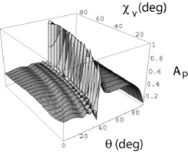
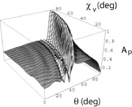
Figures 1, 2, and 3 show as a function of for different values of for chiral STFs made of tantalum oxide, titanium oxide, and zirconium oxide, respectively. For low values of , is small () in all three figures. As increases for a fixed value of , begins to fluctuate, then records a very high value, and then tends to zero as . The sharp –peak indicates the excitation of a surface–plasmon wave at the interface of the metal and the chiral STF [1].

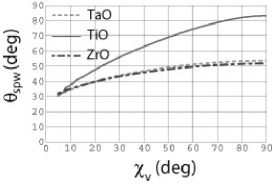
Let denote the value of at which the surface–plasmon wave is excited. Figure 4 contains plots of versus gleaned from the previous three figures. Clearly, as increases, so does for chiral STFs fabricated with a specific evaporant species. But the wavenumber of the surface–plasmon wave is given by
| (11) |
Hence, is a monotonically increasing function of , which means that the phase speed
| (12) |
is a monotonically decreasing function of . This conclusion agrees qualitatively with earlier studies wherein CTFs were considered in lieu of chiral STFs [17, 18].
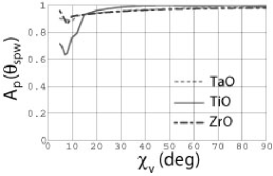
Figure 5 contains plots of at versus gleaned from Figs. 1–3. As increases, the conversion of the incident energy into the energy of the surface–plasmon wave becomes more efficient after an initial drop at very low . There is, however, a threshold value of beyond which the conversion efficiency does not increase appreciably.
Although the numerical results presented in Figs. 1–5 hold strictly for , we have verified that they do not change substantially for other values of . Furthermore, the choice of evaporant species affects the characteristics of the surface–plasmon wave, as is evident from the significantly different graphs in Figs. 4 and 5 for titanium–oxide films than for the other two types of films. This is not surprising because the relative permittivity scalars of the zirconium–oxide and tantalum–oxide films are close to each other but quite different from those of the titanium–oxide films [15].
In conclusion, selection of a higher vapor incidence angle leads to a lower phase speed of the surface–plasmon wave at the planar interface of a metal film and the chiral sculptured thin film, in the Kretschmann configuration. Concurrently, the conversion efficiency of the exciting plane wave into the surface–plasmon wave is higher. Thus, the characteristics of the surface–plasmon wave can be substantially engineered by the proper selection of the vapor incidence angle.
References
- [1] A. Lakhtakia, Surface–plasmon wave at the planar interface of a metal film and a structurally chiral medium, Opt Commun 279 (2007) 291–297.
- [2] T.L. Ferrell, Thin–foil surface–plasmon modification in scanning–probe microscopy, Phys Rev B 50 (1994) 14738–14741.
- [3] J. Homola, S.S. Yee, and G. Gauglitz, Surface plasmon resonance sensors: review, Sens Actuat B: Chem 54 (1999), 3–15.
- [4] J.M. Brockman, B.P. Nelson, and R.M. Corn, Surface plasmon resonance imaging measurements of ultrathin organic films, Annu Rev Phys Chem 51 (2000), 41–63.
- [5] J.M. Pitarke, V.M. Silkin, E.V. Chulkov, and P.M. Echenique, Theory of surface plasmons and surface–plasmon polaritons, Rep Prog Phys 70 (2007), 1-87.
- [6] S. Chandrasekhar, Liquid crystals, Cambridge University Press, Cambridge, United Kingdom, 1992.
- [7] A. Lakhtakia and R. Messier, Sculptured thin films: Nanoengineered morphology and optics, SPIE Press, Bellingham, WA, 2005.
- [8] E. Kretschmann and H. Raether, Radiative decay of nonradiative surface plasmons excited by light, Zeit Naturforsch A 23 (1968), 2135–2136.
- [9] D.O. Smith, M.S. Cohen, and G.P. Weiss, Oblique–incidence anisotropy in evaporated permalloy films, J. Appl. Phys. 31 (1960), 1755–1762.
- [10] R. Messier, A.P. Giri, and R.A. Roy, Revised structure zone model for thin film physical structures, J Vac Sci Technol A 2 (1984), 500–503.
- [11] H. van Kranenberg and C. Lodder, Tailoring growth and local composition by oblique–incidence deposition: a review and new experimental data, Mater Sci Eng R 11 (1994), 295–354.
- [12] N.O. Young and J. Kowal, Optically active fluorite films, Nature 183 (1959), 104–105.
- [13] R. Messier, V.C. Venugopal, and P.D. Sunal, Origin and evolution of sculptured thin films J Vac Sci Technol A 18 (2000), 1538–1545.
- [14] I.J. Hodgkinson, Q.h. Wu, and J. Hazel, Empirical equations for the principal refractive indices and column angle of obliquely deposited films of tantalum oxide, titanium oxide, and zirconium oxide, Appl Opt 37 (1998), 2653–2659.
- [15] F. Chiadini and A. Lakhtakia, Gaussian model for refractive indexes of columnar thin films and Bragg multilayers, Opt Commun 231 (2004), 257–261; corrections: 265 (2006), 366.
- [16] A. Lakhtakia, Pseudo–isotropic and maximum–bandwidth points for axially excited chiral sculptured thin films, Microw Opt Technol Lett 34 (2002), 367–371.
- [17] A. Lakhtakia and J.A. Polo, Jr., Morphological influence on surface–wave propagation at the planar interface of a metal film and a columnar thin film, Asian J Phys (accepted for publication, 2007); also: arXiv:0706.4306.
- [18] J.A. Polo, Jr. and A. Lakhtakia, Morphological effects on surface plasmon polaritons at the planar interface of a metal and a columnar thin film, Microw Opt Technol Lett (submitted for publication, 2007); also: arXiv:0708.2108.