Electronic address:]kchang@semi.ac.cn
Intrinsic Spin Hall Effect Induced by Quantum Phase Transition in HgCdTe Quantum Wells
Abstract
Spin Hall effect can be induced both by the extrinsic impurity scattering and by the intrinsic spin-orbit coupling in the electronic structure. The HgTe/CdTe quantum well has a quantum phase transition where the electronic structure changes from normal to inverted. We show that the intrinsic spin Hall effect of the conduction band vanishes on the normal side, while it is finite on the inverted side. This difference gives a direct mechanism to experimentally distinguish the intrinsic spin Hall effect from the extrinsic one.
pacs:
72.25.-b; 73.63.-b; 71.70.Ej; 85.75.-dSpin-polarized transport in nonmagnetic semiconductors is a crucial ingredient for realizing spintronic devices.Spintronics The spin Hall effect (SHE) opens up the promising prospect of generating spin currents in conventional semiconductors without applying external magnetic field or introducing ferromagnetic elements. Recently the previously predicted extrinsic SHE (ESHE)ESHE and the newly discovered intrinsic SHE (ISHE)ISHE have become one of the most intensively studied subjects. The experimental observations of SHE have been reported by two groupsAwschalomSHE ; WunderlichSHE in n-type epilayers and two-dimensional electron and hole gases, although their theoretical interpretation as extrinsic or intrinsic are still ambiguous.SCZhang2DHG ; RashbaESHE ; DasSarmaESHE The ISHE in the 2D hole gas has no vertex correction,SCZhang2DHG , and its existence has been widely accepted,SHESummary the existence of electron ISHE in two-dimensional systems is under substantial debate.InoueHalperinHaldane ; MacdonaldALL ; RashbaSumRuleRaimondi ; EOMArgument ; Khaetskii ; Nonideal The current understanding is that the electron ISHE in the ideal model (single-band Hamiltonian with parabolic dispersion and linear Rashba and/or Dresselhaus spin splitting) is exactly cancelled by the impurity induced vertex corrections in the clean limit,InoueHalperinHaldane ; MacdonaldALL even for momentum dependent scattering.RashbaSumRuleRaimondi ; EOMArgument ; Khaetskii
Very recently quantum spin Hall effect was predicted theoretically and observed experimentally in a narrowgap HgTe quantum well with the unique inverted band structureZhang . The HgTe quantum well has a quantum phase transition when the quantum well thickness is tuned across a critical thickness . For , the electronic structure is normal, similar to the GaAs quantum wells, where the conduction band has character, and the valence band character. In this regime, we show that the ISHE vanishes in the conduction band due to vertex corrections, consistent with previous results. For , the electronic structure is inverted, where the conduction and the valence bands interchange their characters. In this regime, we show that the ISHE is finite in the conduction band. Since the impurity configuration is not expected to change drastically across , the difference of the SHE across the transition therefore singles out the ISHE contribution. This mechanism solves a long standing challenge of how to distinguish the ISHE from the ESHE.
First we develop a unified description of -electron and -hole SHE based on a general -band effective-mass theory, which remains valid over the whole range of - coupling strengths and bandgaps. Then we take the = model (the Kane model) to make a realistic calculation of the ISHE in CdTe/CdxHg1-xTe quantum wells, taking into account the non-ideal factors in a self-consistent way and the impurity scattering induced vertex corrections through standard diagrammatic techniques. The calculated ISHE agrees with previous theories in the limit of weak - coupling, while it shows nontrivial behaviors in the strong coupling regime. It exhibits a large [ times larger than the intrinsic value ] abrupt increase accompanying the - phase transition in the lowest conduction band. This large ISHE is robust against impurity scattering induced vertex corrections. By varying the well width or the electric bias across the quantum well, we can switch the electron ISHE on/off or even tune it into resonance. These operations can be realized in experimentally accessible conditions and they may be utilized to distinguish the electron ISHE from the ESHE.
Following the new envelope function approach,Burt the band-edge Bloch basis is classified into relevant bands and infinite irrelevant bands . In the -dimensional subspace, the image of the Hamiltonian for a general microstructure is .Burt The image of an arbitrary operator ) can also be obtained as
| (1) |
where and are, respectively, the image of and in the space. Then the images of velocity , spin , and spin current operators are given by , , and .noteOperator With the - coupling taken into account, they generalize the previous theories (which neglect this coupling) to the -band case, e.g., the widely used single-band (four-band Luttinger-Kohn) model corresponds to = =. We emphasize that explicit consideration of the - coupling is important in determining electron ISHE, especially for strong - coupled systems. Further, the different non-ideal band structure factors arise from the same origin (- coupling), so they are not independent and should be incorporated self-consistently through explicit consideration of the - coupling. We notice that the equation-of-motion argumentEOMArgument (valid for =) for the nonexistence of electron ISHE is not applicable to other values of (e.g., =, or ).
The above theory can be applied to study both ISHE and ESHE in a general microstructure. In the present work we consider ISHE only, due to its much larger magnitude compared to ESHE,RashbaESHE ; DasSarmaESHE especially for small electron density. The linear response spin Hall conductivity , with the sample area and the impurity-averaged retarded correlation function of and . Using standard diagrammatic perturbation theory, is evaluated taking into account the impurity induced self-energy corrections in the self-consistent Born approximation and vertex corrections in the ladder approximation (inset of Fig. 1), yielding
where , , and are, respectively, matrix elements of the impurity-averaged Matsubara Green’s function and dressed velocity vertex in the eigenstate basis of . They can be calculated from the Dyson equation and the vertex equation
where is the impurity concentration, and is the matrix element of the single-impurity potential .
Now we consider the lattice-matched symmetric CdTe/CdxHg1-xTe quantum well under electric bias. Its bandgap can be tuned in a large range by varying the Cd content , the well width , or the bias electric field , serving as an ideal workbench for studying ISHE under various - coupling strengths. For such narrowgap systems, the = Kane model is a good starting point. It incorporates the aforementioned non-ideal factors non-perurbatively and self-consistently. The Dresselhaus spin-orbit coupling is neglected because it is much smaller than the Rashba effect in a narrowgap quantum well,LommerSIA as verified by the quantitative agreement between theory and experiment in recent investigations on the transport properties of CdTe/HgTe quantum wells.XCZhangHgCdTe We also adopt the widely employed axial approximation (good for electrons and reasonable for holes in narrowgap systems) and short-range impurity potential . All band parameters used in our numerical calculation are experimentally determined values.XCZhangHgCdTe ; LB We take the temperature = K and, unless specified, the effective disorder strength eV2 Å3, corresponding to typical electron (hole) self-energy broadening 0.1 meV (1 meV) and collisional lifetime 6 ps (0.6 ps).
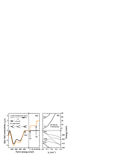
First we consider the weak - coupling case = with Eg(Hg0.63Cd0.37Te)0.4 eV (Fig. 1). Without vertex corrections, the electron ISHE exhibits step-like increases (by approximately one universal value ) at the edges of the first (E1) and second (E2) conduction bands. Such behavior is greatly suppressed by the inclusion of vertex corrections, in sharp contrast to the hole ISHE, which has an opposite sign and remains largely unaffected by vertex corrections. Therefore in the weak coupling regime, the results of the previous theories are recovered.
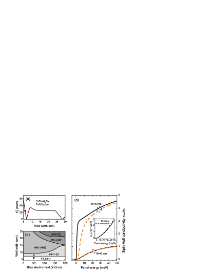
To explore electron ISHE in the strong coupling regime, we consider the CdTe/HgTe quantum well corresponding to =. Due to the abnormal positions and effective masses of the electron and light-hole bands in the HgTe layer, the bandgap of the quantum well at = can be tuned by varying the well width or the electric bias. Fig. 2(a) shows that the derivative of is discontinuous at , and nm, indicating certain phase transitions. Actually, the first critical point at nm corresponds to the normal-inverted phase transition E1-HH1 HH1-E1.CVinvert Namely, the lowest conduction (highest valence) band changes from E1 to HH1 (HH1 to E1), where E (HH) denote electron ( heavy-hole) states. Other critical points corresponds to similar transitions [Fig. 2(b)]. They manifest the red (blue) shift of electron states E2, E3, (heavy-hole states HH1, HH2, ) with increasing well width/electric bias due to weakening of the confinement/quantum confined Stark effect. From Fig. 2(c), we see that in the E1-HH1 phase, arising from the lowest conduction band (E1) is largely cancelled by vertex corrections, especially for small Fermi energy. In contrast, in the HH1-E1 phase, the lowest conduction band (HH1) takes on pure symmetry at small wave vectors and its contribution to is largely unaffected,noteMacdonald leading to the abrupt increase of accompanying the phase transition from E1-HH1 to HH1-E1. This phase transition induced ISHE is robust against impurity induced vertex corrections since it varies only slightly when is increased by an order of magnitude, i.e., when typical electron lifetime [mobility] decreases from 6 to 0.6 ps [ to cmV s]. By changing the well width, large electron ISHE can be switched on/off, especially for small Fermi energy or electron density [inset of Fig. 2(c)].
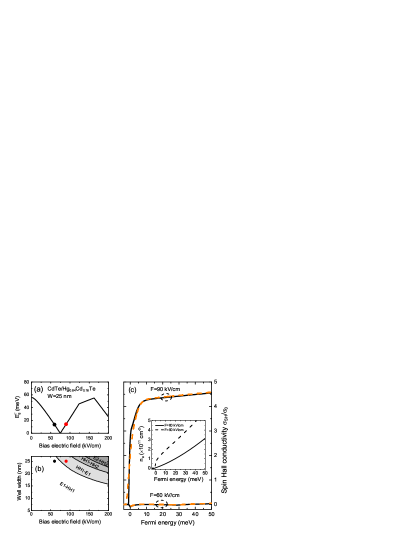
In the above, the phase transition occurs at small critical well width and the electric bias plays a minor role. When the critical well width increases, the bias electric field induced quantum-confined Stark effect would become strong enough to induce the phase transition E1-HH1 HH1-E1 and control the appearance of large electron ISHE. To demonstrate this, we consider the case = with Eg(Hg0.84Cd0.16Te)0. For = nm, the bandgap meV at =0 and decreases to zero at kV/cm [Fig. 3(a)]. The discontinuities of its derivative at , and kV/cm clearly manifest the phase transitions plotted in Fig. 3(b). As a result, in Fig. 3(c) shows a large increase when the bias electric field is tuned across the critical point. Again, the slight dependence on the disorder strength manifests the robustness of the ISHE against impurity induced vertex corrections. The field-induced phase transition provides a dynamic way to switch on/off the electron ISHE, especially for small Fermi energy or electron density [inset of Fig. 3(c)].
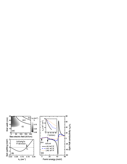
Turning back to CdTe/HgTe quantum wells, Fig. 2(a) shows that the electric bias can induce the transition HH1 E2 in the lowest conduction band or, equivalently, the transition E2 HH1 in the second conduction band [Fig. 4(a)]. In the E2 phase, the Rashba spin splitting between the two branches of the second conduction band reverses its sign at a critical wave vector [Fig. 4(b)]. Analysis shows that this behavior comes from the coupling between the two branches and the interface states,ShamInterfacial thus it does not exist in the HH1 phase. By varying the well width or electric bias, such behavior can be switched on/off [Fig. 4(a)] and the critical wave vector [gray scale map in Fig. 4(a)] or critical electron density [inset of Fig. 4(c)] can be tuned, offering us the possibility to manipulate the ISHE arising from the second conduction band. Indeed, in Fig. 4(c) exhibits a resonance when the Fermi energy coincides with the spin degeneracy point.
We notice that although such level-crossing induced resonance has been predicted for the widely accepted hole ISHE in p-type GaAs quantum wells (based on calculations that neglect vertex corrections),holeISHEResonant similar prediction for the much debated n-type systems still remains absent. For hole ISHE, a challenging hole lifetime 10 ps or hole mobility cm2/(V s) is required to observe the resonance.holeISHEResonant For electron ISHE, the requirement is significantly relaxed to electron lifetime ps [corresponding to eV2 Å3, cf. Fig. 4(c)] or electron mobility cm2/(V s). These have already been realized in previous experiments, e.g., = cmV s for = nmHgTemobility1 and = cmV s for = nmXCZhangHgCdTe (close to the well width used in our calculation).
In summary, we have investigated the electron ISHE in narrowgap HgCdTe quantum wells based on a unified description for electron and hole ISHE. While the ISHE of the conduction band vanishes on the normal side of the - phase transition, a ISHE in the conduction band can be generated on the inverted side. It is robust against impurity induced vertex corrections. By changing the Cd content, the well width, or the bias electric field, we can switch the ISHE on/off or tune it into resonance under experimentally accessible conditions. Ref. Hankiewicz shows that the spin Hall effect can be experimentally observed by the non-local transport measurements in mesoscopic systems. We propose to carry out such measurement for both the normal and inverted quantum wells, both close to the transition. The difference uniquely singles out the ISHE contribution.
This work is supported by the NSFC Grant No. 60525405, the knowledge innovation project of CAS, the NSF under grant numbers DMR-0342832 and the US Department of Energy, Office of Basic Energy Sciences under contract DE-AC03-76SF00515.
References
- (1) S. A. Wolf et al., Science 294, 1488 (2001).
- (2) M. I. D’yakonov and V. I. Perel’, Phys. Lett. A 35, 459 (1971); J. E. Hirsch, Phys. Rev. Lett. 83, 1834 (1999).
- (3) S. Murakami, N. Nagaosa, and S. C. Zhang, Science 301, 1348 (2003); J. Sinova et al., Phys. Rev. Lett. 92, 126603 (2004).
- (4) Y. K. Kato, R. C. Myers, A. C. Gossard, and D. D. Awschalom, Science 306, 1910 (2004); V. Sih et al., Nature Phys. 1, 31 (2005); V. Sih et al., Phys. Rev. Lett. 97, 096605 (2006); N. P. Stern et al., Phys. Rev. Lett. 97, 126603 (2006).
- (5) J. Wunderlich, B. Kaestner, J. Sinova, and T. Jungwirth, Phys. Rev. Lett. 94, 047204 (2005).
- (6) B. A. Bernevig and S. C. Zhang, Phys. Rev. Lett. 95, 016801 (2005).
- (7) H. A. Engel, B. I. Halperin, and E. I. Rashba, Phys. Rev. Lett. 95, 166605 (2005).
- (8) W. K. Tse and S. Das Sarma, Phys. Rev. Lett. 96, 056601 (2006).
- (9) J. Sinova, S. Murakami, S. Q. Shen, and M. S. Choi, Solid State Commun. 138, 214 (2006); and references therein.
- (10) E. G. Mishchenko, A. V. Shytov, and B. I. Halperin, Phys. Rev. Lett. 93, 226602 (2004); J. Inoue, G. E. W. Bauer, and L. W. Molenkamp, Phys. Rev. B, 67, 033104 (2003); 70, 041303(R) (2004); D. N. Sheng, L. Sheng, Z. Y. Weng, and F. D. M. Haldane, ibid. 72, 153307 (2005).
- (11) K. Nomura, J. Sinova, N. A. Sinitsyn, and A. H. MacDonald, Phys. Rev. B 72, 165316 (2005).
- (12) E. I. Rashba, Phys. Rev. B 70, 201309(R) (2004); R. Raimondi and P. Schwab, ibid. 71, 033311 (2005).
- (13) O. Chalaev and D. Loss, Phys. Rev. B 71, 245318 (2005); O. V. Dimitrova, ibid. 71, 245327 (2005).
- (14) A. Khaetskii, Phys. Rev. Lett. 96, 056602 (2006).
- (15) A. G. Mal’shukov and K. A. Chao, Phys. Rev. B 71, 121308(R) (2005); A. V. Shytov, E. G. Mishchenko, H. A. Engel, and B. I. Halperin, ibid. 73, 075316 (2006); C. M. Wang, X. L. Lei, and S. Y. Liu, ibid. 73, 113314 (2006); P. L. Krotkov and S. Das Sarma, ibid. 73, 195307 (2006).
- (16) D. F. Nelson, R. C. Miller, and D. A. Kleinman, Phys. Rev. B 35, 7770 (1987).
- (17) W. Yang and K. Chang, Phys. Rev. B 73, 113303 (2006); 74, 193314 (2006).
- (18) İ. Adagideli and G. E. W. Bauer, Phys. Rev. Lett. 95, 256602 (2005).
- (19) L. Sheng, D. N. Sheng, and C. S. Ting, Phys. Rev. Lett. 94, 016602 (2005); W. Ren et al., ibid. 97, 066603 (2006); Z. H. Qiao, W. Ren, J. Wang, and Hong Guo, ibid. 98, 196402 (2007).
- (20) B. A. Bernevig, T. L. Hughes, and S. C. Zhang, Sciences 314, 1757 (2006); M. König, Science Express 1148047 (2007).
- (21) M. G. Burt, J. Phys.: Condens. Matter 4, 6651 (1992).
- (22) In obtaining and , we have neglected the second term in Eq. (1), which is smaller than the first term by a factor . This approximation becomes exact when and are chosen such that , e.g., for (single-band model), (six-band Luttinger-Kohn model), and (Kane model).
- (23) G. Lommer, F. Malcher, and U. Rössler, Phys. Rev. Lett. 60, 728 (1988).
- (24) X. C. Zhang et al., Phys. Rev. B 63, 245305 (2001); K. Ortner et al., ibid. 66, 075322 (2002).
- (25) II-VI and I-VII Compounds; Semimagnetic Compounds, Landolt-Börnstein, Group III, Vol. 41B, ed. U. Rössler (Springer-Verlag, Berlin, 1999).
- (26) N. F. Johnson, P. M. Hui, and H. Ehrenreich, Phys. Rev. Lett. 61, 1993 (1988).
- (27) Based on a modified single-band Rashba model instead of the correct heavy-hole Hamiltonian, the conclusion of Ref. MacdonaldALL differs from ours. We believe that in the inverted band phase, single-band results should be taken with cautious due to the strong - coupling.
- (28) Y. R. Lin-Liu and L. J. Sham, Phys. Rev. B 32, 5561 (1985).
- (29) X. Dai, Z. Fang, Y. G. Yao, and F. C. Zhang, Phys. Rev. Lett. 96, 086802 (2006).
- (30) J. R. Meyer et al., Phys. Rev. B 38, 2204 (1988).
- (31) E. M. Hankiewicz, L. W. Molenkamp, T. Jungwirth, and Jairo Sinova, Phys. Rev. B 70, 241301 (2004).