Giant dynamical Zeeman split in inverse spin valves
Abstract
The inversion of a spin valve device is proposed. Opposite to a conventional spin valve of a non-magnetic spacer sandwiched between two ferromagnetic metals, an inverse spin valve is a ferromagnet sandwiched between two non-magnetic metals. It is predicted that, under a bias, the chemical potentials of spin-up and spin-down electrons in the metals split at metal-ferromagnet interfaces, a dynamical Zeeman effect. This split is of the order of an applied bias. Thus, there should be no problem of generating an split that is not possible to be realized on the earth by the usual Zeeman effect.
Spintronics becomes an emergent subfield in condensed matter physics since the discovery of giant magnetoresistance in 1988 by FertFert and GrunbergGrun . Spintronics is about the control and manipulation of both electron charge and electron spin. Many interesting phenomena are related to the interplay between electron spin and its charge degrees of freedom. For example, electron transport can be manipulated by the magnetization configurations. This is the basis of giant magnetoresistanceFert ; Grun ; Parkin and tunneling magnetoresistanceMiyazaki ; Moodera phenomena and devices. Its inverse effect, known as spin-transfer torque (STT)Slon ; Berger ; xrw , was also discovered. The STT opens a new way to manipulate magnetization other than a magnetic fieldxrw1 , which has been much of recent focus in the field due to its potential applications in information storage industry.
In this letter, an inverse spin valve structure of a ferromagnet sandwiched between two non-magnetic metals is studied when a bias is applied to the device. Due to the spin-dependent electron transport of the structure, the chemical potentials of spin-up (SU) and spin-down (SD) electrons at the metal-ferromagnet interfaces split by the magnitude of an applied bias. We term this split dynamical Zeeman effect. This split can be of the order of if proper materials are used. To introduce a similar split by the usual Zeeman effect, a magnetic field unrealizable on the earth is required. Thus, a giant dynamical Zeeman effect is predicted.
A conventional spin valve is a layered structure of a non-magnetic spacer sandwiched between two ferromagnetic metals. The spin valve is called a giant magnetoresistance device if the spacer is a normal metal while it is a tunneling magnetoresistance device for an insulator spacer. The electron transport of a spin valve depends on the relative polarities of the two magnets. An inverse spin valve is also a layered structure with a ferromagnet sandwiched between two non-magnetic metals as illustrated in Fig. 1a. and are two normal metals with identical SU and SD electron density of states (DOS) as depicted schematically in the left and right diagrams of Fig. 1b. To simplify our analysis, a half-metal (HM) spacer is considered first so that only electrons of one type of spins (spin-up) can pass through it. The DOSs of SU and SD electrons for a half-metal is illustrated by the middle diagram of Fig. 1b. Under a bias , SU electrons in flow into the empty SU electron states in via the empty SU electron states in the half-metal, shown pictorially by the curved arrows in Fig. 1b. The flow of the electrons creates chemical potential differences ( in Fig. 1b) between SU and SD electrons in both and near the metal-ferromagnet interfaces.
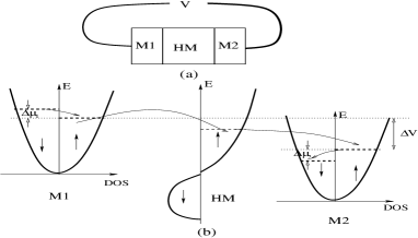
In order to understand why the chemical potentials of SU and SD electrons at the and interfaces split under a bias, let us consider an extreme case in which spin relaxation time in both and is infinite long (no spin relaxation so that SU and SD electrons are isolated from each other). Since electron transport in a nanostructure depends on how a bias is appliedsdwang , we assume, to be precise and without losing generality, that the electron chemical potential in is initially moved up by while that of is kept unchanged. Initially, SU electrons flow into the empty SU electron states in because the half-metal prevent SD electrons from flowing. The same amount electrons will be pumped back from to by a battery to keep the electron neutrality in and . However, a battery does not distinguish electron spin, and as a result it will pump equal amount of SU and SD electrons. In other words, SU electrons flow out of and into via the half-metallic spacer. In the meanwhile, an equal amount of electrons with half of them being in the SU state and the other half in the SD state are drawn out of and are supplied into by the battery. As a result, accumulates more SD electrons, and accumulates more SU electrons. Thus, the chemical potential of the SD electrons will be higher than that of SU electrons in . Vice versa, the chemical potential of the SU electrons will be higher than that of SD electrons in . The chemical potential splits keep increasing until the chemical potential of SU electrons in equals that in . At this point, the steady state with no current in the circuit is reached and chemical potential splits in and are established with .
The spin relaxationt1t2 always exists in a material, and the magnitude of the chemical potential split for SU and SD electrons depends sensitively on the spin relaxation. This sensitivity can be seen from another extreme case that the spin flipping is so fast that SU and SD electrons can be converted into each other any time at no cost (meaning SU and SD electrons are at equilibrium with respect to each others at all times in and ). Thus, it is impossible to create any chemical potential difference for SU and SD electrons in and . The reality, of course, is somewhere in between (the two extreme cases). The spin relaxation time of a real material is finite, and it depends on the strength of spin-orbital coupling, hyperfine interaction and other interactions that cause spin flipping. In order to include the spin relaxation time quantitatively, consider an ideal model at zero temperature. Assume the spin flip occurs only near the interfaces within a width of spin diffusion length in and in . This is justified because both SU and SD electrons in the rest parts of the circuit (other than the half-metal) should have same chemical potential. Thus number of electrons flipped from up-spin state to down-spin state is the same as that from down-spin to up-spin. Furthermore, let us assume the resistance of the half-metal is (for SU electrons, the resistance for SD electrons is infinity due to the half-metallic nature of the middle spacer).

The equations of the motion of the device can be obtained by considering electron flow diagram of Fig. 2. There are two reservoirs in and each. One is for SU electrons, and the other is for SD electrons (denoted by rectangular boxes). SU electrons in can flow into SU electron reservoir of . The current depends on resistance and chemical potential difference (Fig. 1b) of SU electrons in and ,
| (1) |
If one neglects the direct tunneling of SD electron from to through the half-metal ( in Fig. 2), SD electrons can only go to by first flipping their spins and converting themselves into SU electrons. Let and be the spin flipping time (spin-relaxation time t1t2 ) in and , corresponding to the flipping rate of and , respectively. Due to the conversion of SD electrons to SU electrons that is the product of the excess SD electrons and the single electron flipping rate, the current from SD reservoir to SU reservoir in is
| (2) |
where is the density of states of SD electrons in at the Fermi level. is the cross section of . Similarly, the current due to the conversion of SU electrons to SD electrons in is
| (3) |
At the steady state, there is no net electron build up anywhere in the circuit. Since the current through the battery is unpolarized, spin-up electrons will be mixed up with spin-down electrons and be pumped by the battery from into . Thus, the SU electrons make up half of the current while other half is made up from the SD electrons, and the balancing conditions and external constraint require
| (4) | ||||
Solving Eqs. (1), (2),(3), and (Giant dynamical Zeeman split in inverse spin valves), the dynamical Zeeman split and are
| (5) |
It is interesting to see that the largest dynamical Zeeman split occur at , a short circuit for spin-up (SU) electrons! In this particular case, one, of course, needs to use metals with proper material parameters such that current density is not too large to cause the metal breaking down by heating. Further discussions on this issue are given soon.
The half-metal may be replaced by a usual ferromagnetic metal. In this case, SD electrons in can also flow directly into , contributing an extra current to the circuit
| (6) |
where is the resistance of ferromagnet for SD electrons. Without losing generality, the minority carriers of the ferromagnet are assumed to be the SD electrons, and is also assumed to be larger than . The chemical potential difference of SD electrons in and equals as it is shown in Fig. 1b. Eq. (Giant dynamical Zeeman split in inverse spin valves) should be modified accordingly as
| (7) | ||||
This set of equations with non-zero can be solved, and the dynamical Zeeman split and , in comparison with that of half-metal case, are reduced by a factor of
| (8) |
One should not be surprised about this reduction from our early explanations of the origin of this split. Obviously, previous results Eq. (Giant dynamical Zeeman split in inverse spin valves) are recovered when . Also, there are no chemical potential splits in and when the spacer is non-magnetic (). Therefore, a good half-metal (good conductor for the majority carriers and good insulator for the minority carriers) should be used if one wants to maximize the split. In the following discussion, case is considered only.
The conventional way of introducing an energy split for SU and SD electrons is through the Zeeman effect. Due to the small value of Bohr magneton, an order of field can only induce about energy split. However, the dynamical Zeeman split predicted here could easily be of the order of , a truly giant Zeeman effect. Compare with the static Zeeman effect, this split is equivalent to a field in the order of , an impossible magnetic field on the earth!
It is interesting to notice that a large spin-dependent chemical potential difference means a large dynamical magnet. For and a typical electron density of states of for a metal, the dynamical magnetization is about which is comparable with many magnets. Thus one can use MOKE (magneto-optical Kerr effect) to ‘see’ the dynamical magnetization. Upon verification of this dynamical magnetism, it should be interesting to explore the potential applications of this electric-field controlled magnet. Another possible application of the predicted phenomena is polarized electron/light sourcexrw2 . Since electrons of one type of spins occupy higher energy levels than those of the opposite spin, the predicted effect can be used as a polarized electron source, or light source when the electrons flip their spins and emitted well-defined polarized photons. Thus, the phenomenon can be used to make tunable light emitting diode or laser in very wide frequency range. The large chemical potential difference may also be used to enhance electron magnetic resonance signal. The electron magnetic resonance is useful in probing material properties in various technologies with wide applications, including imaging in information processing.
It should be pointed out that we have not considered the spatial distribution of the chemical potential split. Our results may be modified quantitatively, but not qualitatively, when the detailed distribution is taken into account. This is because a factor characterized the distribution should be added to equations (3) and (4). It should also be noted that the giant dynamical Zeeman split reported here is different from the split in the DOS of a ferromagnet. In the usual ferromagnets, electron DOS is spin dependent, but the chemical potential of both SU and SD electrons are the same at the equilibrium. However, the dynamical Zeeman split predicted here occurs inside a non-magnetic metal where the electron DOS is spin-independent, but the spin-up and spin-down electrons fill their DOSs to different levels, leading to a chemical potential difference.
In conclusion, we propose an inverse spin valve structure consisting of a ferromagnet sandwiched between two normal metals. Under a bias, we predicted a giant dynamical Zeeman split of the chemical potential for spin-up electrons and spin-down electrons at metal-ferromagnet interfaces. This prediction is yet to be confirmed by experiments.
The author would like to thank Prof. Yongli Gao and Prof. John Xiao for the useful discussions. This work is supported by UGC, Hong Kong, through CERG grant (# 603007 and SBI07/08.SC09).
References
- (1) M.N. Baibich, J.M. Broto, A. Fert, F.N. Van Dau, F. Petroff, P. Etienne, G. Creuzet, A. Friederich, and J. Chazelas, Phys. Rev. Lett. 61, 2427 (1988).
- (2) G. Binach, P. Grunberg, F. Saurenbach, and W. Zinn, Phys. Rev. B 39, 4828 (1989).
- (3) R.F.C. Farrow, C.H. Lee, and S.S.P. Parkin, IBM J. Res. Dev. bf 34, 903 (1990).
- (4) T. Miyazaki and N. Tezuka, J. Magn. Magn. Mater. 139, L231 (1995).
- (5) J.S. Moodera et al., Phys. Rev. Lett. 74, 3273 (1995).
- (6) J.C. Slonczewski, J. Magn. Magn. Mater. 159, L1-L7 (1996).
- (7) L. Berger, Phys. Rev. B 54, 9353 (1996).
- (8) X.R. Wang, and Z.Z. Sun, Phys. Rev. Lett. 98, 077201 (2007).
- (9) Z.Z. Sun, and X.R. Wang, Phys. Rev. Lett. 97, 077205 (2006); Phys. Rev. B 71, 174430 (2005); ibid 73, 092416 (2006); ibid 73, (2007); T. Moriyama, R. Cao, J.Q. Xiao, J. Lu, X.R. Wang, Q. Wen, and H.W. Zhang, Appl. Phys. Lett. 90, 152503 (2007).
- (10) S.D. Wang, Z.Z. Sun, N. Cue, H.Q. Xu, and X.R. Wang, Phys. Rev. B 65, 125307 (2002).
- (11) X.R. Wang, Y.S. Zheng, and S. Yin, Phys. Rev. B 72, R121303 (2005).
- (12) X.R. Wang, unpublished.