Influence of slab thickness on the Casimir force
Abstract
We calculate the Casimir force between slabs of finite thickness made of intrinsic and doped silicon with different concentration of carriers and compare the results to those obtained for gold slabs. We use the Drude and the plasma models to describe the dielectric function for the carriers in doped Si. We discuss the possibility of experimentally testing the appropriateness of these models. We also investigate the influence of finite thickness on , which has recently been proposed for Casimir effect measurements testing the metal-insulator transition.
pacs:
42.50.Ct,12.20.Ds,12.20.-mI Introduction
The availability of experimental set-ups that allow accurate measurements of surface forces between macroscopic objects at submicron separations has recently stimulated a renewed interest in the Casimir effect Casimir and its possible applications to micro- and nanotechnology.
In 1948 H. Casimir calculated the force between two plane-parallel mirrors placed in vacuum at a distance apart from each other and with the area of the mirrors being much larger than the squared distance . In the ideal case of perfectly reflecting mirrors the force is given by the following expression
| (1) |
with a positive value of corresponding to attraction, and a subsequent negative pressure.
The Casimir force can be understood as the effect of radiation pressure on the Fabry-Perot cavity formed by the two plane and parallel mirrors. The intracavity vacuum energy being either enhanced or suppressed, depending on whether the field frequency is resonant or antiresonant, the net Casimir force results from the balance between the repulsive and attractive contributions associated respectively with these frequencies. The force is then obtained as an integral over the axis of real frequencies, including the contribution of evanescent waves besides that of ordinary waves, and transformed into an integral over imaginary frequencies by using physical properties fulfilled by real mirrors used in experiments which do not require any further adhoc hypothesis.
Compared to the ideal situation considered by Casimir, a number of corrections have to be taken into account in the calculation of the force in real experiments. A large number of papers have been devoted to the study of these effects and we refer the reader to Bordag01 for an extensive bibliography. Here we will only be concerned by the influence of the material properties and slab thickness.
Considerable experimental progress has been achieved Bordag01 in the control of the Casimir effect, opening the way to applications in nano-science roukes ; capasso , particularly in the development of nano- or microelectromechanical devices (NEMS or MEMS). NEMS are movable nano mechanical structures inspired from MEMS, with minimal critical dimensions of a few tens to a few hundreds nanometers. NEMS approach constitutes a real technological breakthrough to prepare the future generations of sensors and actuators. At such small distances between the different elements, the Casimir force in these systems may become quite important. It may, on one hand, perturb the systems and produce stiction and adhesion roukes , but also be put to good use as an external force allowing to change the systems’ resonance frequency or introduce bistable behavior capasso .
In the past 10 years the Casimir effect has been studied extensively for metals. Experiments have been performed for Au, Al, Cu in different geometries and experimental set-ups. On the theoretical side, calculations have taken into account the finite conductivity and frequency dependent reflection coefficient of the different metals, modeling them either by plasma or Drude model or taking into account tabulated optical dataLambrecht00 ; Genet00 ; Bordag01 ; Genet02 ; Jaekel91 ; Pirozhenko06 . Only recently, a Casimir force measurement for Silicon bulk mirrors has been reported on Mohideen06 ; Mohideen07 and calculations of the Casimir force for Si bulks and slabs Esquivel03 ; AndreucciPLA have been performed however without investigating further the observed difference in the bulk and slab behavior. The temperature dependence of the force between Si plates has been studied in Inui03 , while the influence of skin depth on the Casimir force between metallic surfaces has been observed recently by Capasso and collaborators PNAS .
The reference material in nano- or micro-electromechanical devices is of course Silicon. In this paper, we present calculations of the Casimir force between slabs of intrinsic or doped Silicon, Gold and VO2. In particular, we concentrate on the influence of the slab thickness on the value of the force. We use the Drude and the plasma model for the dielectric function of conductors and a Drude-Lorentz model for Si and the insulating VO2. We have previously shown that for intrinsic Silicon the Casimir force depends strongly on the slab thickness and reduces considerably if the slab separation exceeds the slab thickness, while for Gold force reduction is negligible, except for very thin slabs LPDA . If the conductor is modeled by a plasma model () the Casimir force becomes independent of the slab thickness. Our present calculations show that for doped Silicon, the Casimir force is diminished only in some distance range and for low carrier levels and re-increases at long distances. We explain these effects by analyzing the phase factor acquired by the vacuum field due to finite slab thickness and the different behavior of the dielectric functions. We also discuss the effect of a Gold coating on the Si slab. Even though, a description of a thin Gold film by a local dielectric function is not completely reliable anymore, it gives some hint about the expected behavior. The slightest Gold coating on intrinsic Silicon, even of only 1nm thickness, re-increases the Casimir force between the two Si slabs. The above described decrease in the force due to finite thickness of the Si slab vanished because of the Gold coating.
We finally analyze the influence of slab thickness for VO2 which has the particularity to undergo a metal-insulator transition at 340 K Verleur1968 ; Dachuan . An experiment was proposed recently Mohideen07a to investigate in detail the temperature dependence of the Casimir force between gold and VO2 film. The temperature dependence of the Casimir effect is still an issue of controversial discussions Bostrom00 ; Svetovoy00 ; Bordag00 ; Lamoreaux01c ; Sernelius01r ; Sernelius01c ; Bordag01r ; Klimchitskaya01 ; Hoye03 ; Brevik05 ; Bezerra05 ; Buenzli05 ; Jancovici05 ; Brevik06 ; Brevik07 . Here we make account only of the crucial change in the conductivity due to the phase transition, but do not consider the temperature corrections to the Casimir effect itself.
II Formulation of the Casimir force between slabs of finite thickness
The Casimir force is usually written as an integral over imaginary frequencies and wavevectors Lifshitz1 . In order to visualize easily the variation of the real Casimir force with respect to the ideal formula (1) it is convenient to introduce a reduction factor Lambrecht00
| (2) | |||
denotes the reflection amplitudes of the mirrors at a given polarization . This notation is a shorthand for where is the imaginary frequency and the imaginary wavevector along the longitudinal direction of the cavity while is the modulus of the transverse wavevector. The second integral is written over imaginary frequencies as explained in detail in Lambrecht00 .
Assuming the plates to have a large optical thickness, the reflection coefficients correspond to the ones of a mere vacuum-metal interface LandauECM9
| (3) |
stands for and is the dielectric constant of the metal evaluated for imaginary frequencies.
However, for thin mirrors or slabs the reflection coefficients depend on the physical thickness and evaluate to LambrechtPLA97 ; Genet03 ; PNAS ; Lambrecht06
| (4) |
is the dielectric function of the material evaluated for imaginary frequencies. is the optical length of the slab. The single interface expression is recovered in the limit of a large optical thickness .
The dielectric response function for real frequencies may be written in terms of real and imaginary parts and obeying usual causality relations which allow one to obtain the dielectric constant at imaginary frequencies from the function evaluated at real frequencies LandauECM9
| (5) |
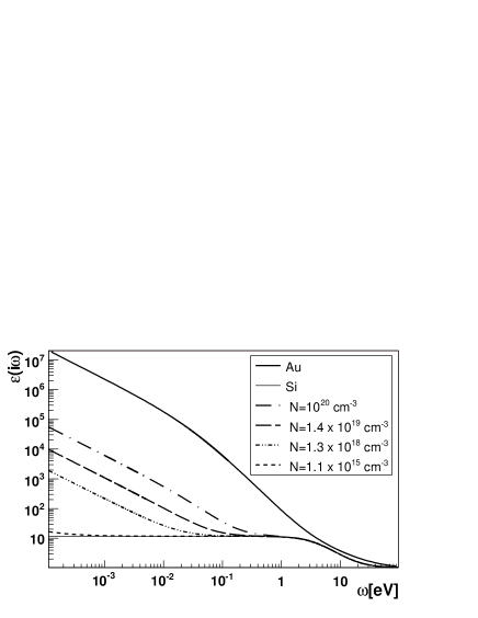
The tabulated optical data for the complex index of refraction for Silicon and Gold can be found in Palik , while the data for VO2 has been given in a dedicated paper Verleur1968 . For Silicon and VO2 the data covers the whole relevant frequency range and, in contrast to most metals, no extrapolation procedure at low frequencies is necessary. We will give frequencies either in V or in rad/s, using the equivalence 1 V rad/s. Figure 1 shows the dielectric permeability of doped Silicon with different carrier concentrations as a function of imaginary frequencies, obtained by using (5), which we will need for the calculation of the reduction factor of the Casimir force (2). While at low-frequencies the dielectric function of intrinsic Silicon approaches a constant value , of doped Si increases with increasing carrier concentration and behaves like that of diluted metal. With increasing frequency, the dielectric function of intrinsic Silicon is nearly constant up to about rad/s and falls off only for high frequencies above a cut-off frequency, rad/s, towards its asymptotic value . of doped Silicon decreases rapidly with increasing frequency and shows the same cut-off frequency as intrinsic Si.
The dielectric function of intrinsic Silicon can well be approximated by the following Drude-Lorentz function Bergstrom97
| (6) |
with the numerical values as given above. The dielectric function of doped Si contains an additional part, which is modeled with a dielectric function given by a Drude model
| (7) |
The different values of the plasma frequency and the relaxation rate for various carrier densities are given in Table 1.
| N () | (eV) | (eV) | ( cm) |
|---|---|---|---|
| 13 | |||
The description of the dielectric function of the p-doped Silicon by the model (7) is valid for the doping levels up to cm-3. For higher doping levels Si becomes degenerated.
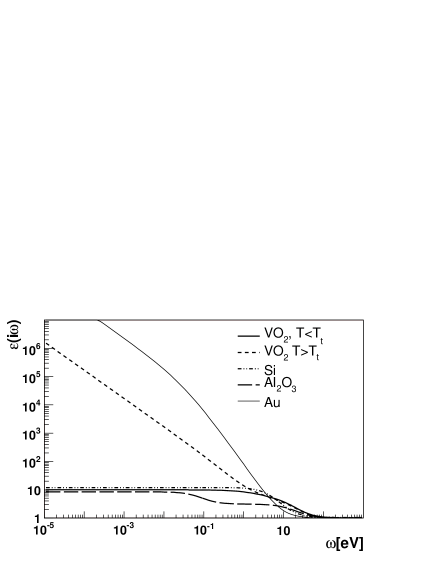
The dielectric function of VO2 is shown in Fig. 2 above and below the critical temperature . Below the critical temperature we used the model already applied in Mohideen07a which had been proposed first in Verleur1968
| (8) |
with , . For the rest of the parameters see Table 2. Above the critical temperature the dielectric permeability is given by
| (9) | |||||
where , eV, eV.
| (eV) | ||
|---|---|---|
| 0.79 | 1.02 | 0.55 |
| 0.474 | 1.30 | 0.55 |
| 0.483 | 1.50 | 0.50 |
| 0.536 | 2.75 | 0.22 |
| 1.316 | 3.49 | 0.47 |
| 1.060 | 3.76 | 0.38 |
| 0.99 | 5.1 | 0.385 |
| (eV) | ||
|---|---|---|
| 1.816 | 0.86 | 0.95 |
| 0.972 | 2.8 | 0.23 |
| 1.04 | 3.48 | 0.28 |
| 1.05 | 4.6 | 0.34 |
Clearly, above the critical temperature the material behaves more like a metal with a strongly increasing dielectric function at low frequencies. For low temperatures its dielectric function nearly matches the one of intrinsic Si, as VO2 becomes an insulator and the dielectric function at zero frequency has a constant value of about .
III Numerical results for doped Silicon
We now evaluate the Casimir force (2) using the tabulated optical data for different slab thickness . The numerical procedures follow the principles described in Lambrecht00 .
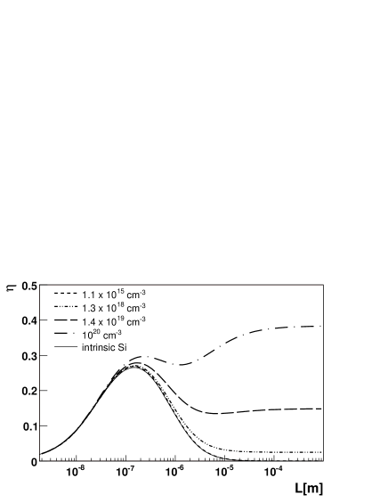
Figures 3 and 4 show as a function of plate separation for intrinsic and p-doped Silicon for bulk mirrors and for Si slabs of 100nm thickness. Between two bulk mirrors the force reduction factor is a continuously growing function of the mirror separation and reaches a constant value in the long distance limit, which means that . In contrast, between two Silicon slabs the Casimir force reduction factor grows continuously only for separations , while it starts to diminish considerably when the slab separation becomes of the order of or exceeds the physical slab thickness LPDA . This effect disappears for doped Silicon. Only a small decrease in the force reduction factor remains at intermediate distances (about 1m). For larger distances the conduction due to the carriers introduced by doping re-increases the value of the reduction factor.
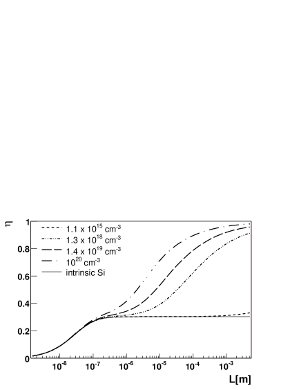
This result could have very interesting consequences in nanotechnology. The observed decrease in the Casimir force for intrinsic Si in the distance range can be canceled by injecting carriers. This allows to tune the Casimir force within certain restrictions using at the same time the slab thickness and the carrier densities as variable parameters.
In Mohideen07 the first experiment of optical modulation of dispersion forces through the change of carrier density by laser pulses was reported. The irradiation of a silicon slab by laser pulses allows to achieve charge carrier concentrations of cm-3. Here we present numerical results for the Casimir force obtained by assuming that the contribution of the induced charge carriers is given by Drude or plasma terms, or , , with eV, eV for the positive induced carriers and eV, eV for the negative ones.
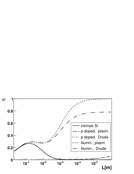
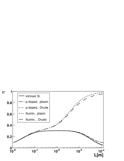
Fig. 5 gives the numerical results for the reduction factor of Casimir force between two silicon slabs irradiated by laser pulses in comparison with p-doped silicon. Here we took the parameters from the paper Mohideen07 . The doping is described by the Drude or plasma model. The difference between the models could manifest itself at distances of several micrometers for highly doped silicon provided the slab is thin (upper graph). However the experiment requires a mirror thick enough for irradiation not to penetrate into the cavity. The thickness should be greater than the optical absorption depth of Si at the wavelength of the laser beam used for the doping. If the thickness of the slab is 4000 nm as used in Mohideen07 the experiment can hardly distinguish between Drude and plasma models.
IV Numerical results for VO2
In Mohideen07a a compound mirror, having a 100nm layer of VO2 on an Al2O3 bulk substrate, is treated as an effective medium with a dielectric permittivity (8,9). The authors rely on the fact that the parameters in Table 2 were retrieved from reflectivity and transmissivity spectra exactly for the same two-layered system as in Ref. Verleur1968 .
However, Verleur1968 contains also the description of the fitting procedure that uses the formulas corresponding to two layered system. The finite thickness of the substrate is neglected in the analysis, but the account is made for the finite thickness of the VO2 film. The dielectric function of the substrate (sapphire) is considered as known. It is substituted into the formulas, and the unknown parameters of the model describing the VO2 film are found by the curve fitting programme. Since it is not quite clear from Verleur1968 if the parameters in the Table 2 and the model correspond to the effective media or to the itself, we considered both possibilities.
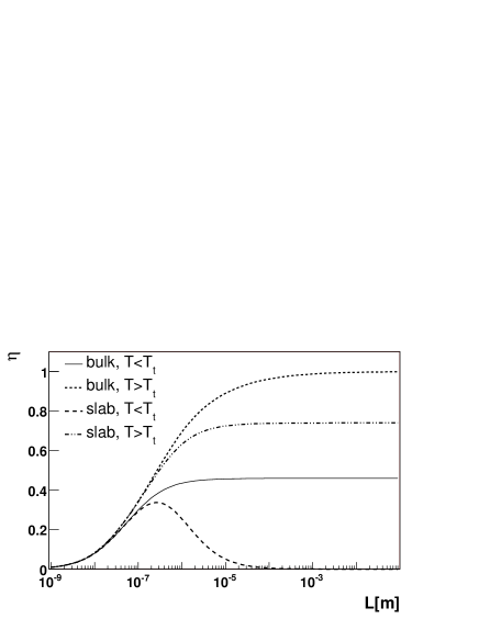
First we calculated the reduction factor for the Casimir force between two ”bulks” of the effective medium. In other words we use the dielectric permittivities (8) and (9) with the parameters from Table 2 and formulas for bulk reflection coefficients. The corresponding curves in Fig. 6 are plotted by thin full line below the phase transition, , and by thick full line above it, .
The reduction factor for the Casimir force between two 100 nm VO2 slabs below the phase transition is given by thin dotted line. We see that before the phase transition the behavior of VO2 slabs resembles the one of the silicon slabs. Above the phase transition (, thick dotted line) the material behaves like a dilute metal, and we do not observe the decrease of the reduction factor at nm. However the reduction factor for a slab never reaches the unit value it does for pure metals at zero temperature in the long distance limit.
We also calculate the reduction factor for nm VO2 film on a sapphire substrate. It means that we used the formulae for two-layered mirrors. The layer facing the cavity has the dielectric permittivity (8) at and (9) at . For the substrate we used the dielectric permittivity of Al2O3
with , , , and eV, eV, eV mellesgriot .
Below the transition temperature the dielectric function of VO2 is close to the one of Al2O3 (see Fig. 2). That is why the result for the Casimir force between two effective media bulks almost coincides with the force between two-layered mirrors, VO2 on sapphire substrate. When the temperature overpasses the critical value, the entire bulk of the effective media becomes a metal, while in the case of two-layered mirror, the substrate remains an insulator. Consequently, at large distances the force between two effective media bulks is larger than the force between compound mirrors. The force obtained within the effective media calculation differs from the result of the two-layer calculation starting from the distance of several hundred nanometers (Fig. 6).
Finally in Fig. 7 we present the results for the VO2 mirror in front of the Gold mirror. The curves obey the same distance dependencies as in the case of equal mirrors. But the values of the reduction factor are increased thanks to the high reflectivity of gold. This setup is favorable from the experimental point of view.
It is important to note that the dielectric function we use corresponds to thin film measurements. If the force is measured between true bulk VO2 mirrors, the results should be compared with the calculation that uses the bulk dielectric function Verleur1968 .
V Discussion and Conclusion
The obtained results can be understood in terms of the optical length of the layer material or the phase factor acquired by the field while propagating through the finite layer.

As indicated in (4), the phase factor is frequency-, wavevector- and thickness-dependent. Using the dielectric function of Silicon, which is typical for insulators, in expression (4) we find
| (10) |
The phase factor (4) for metals or doped Si slabs modeled by a Drude or plasma model () evaluates to
| (11) |
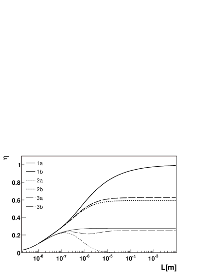
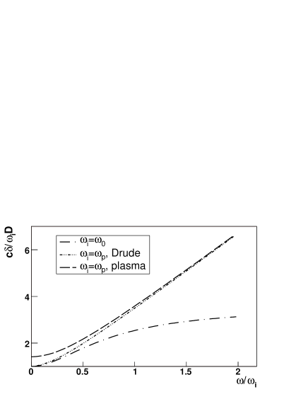
Let us now compare these phase factors at some constant fixed value for , and . Fig. 8 shows the phase acquired by the vacuum field while propagating through the intrinsic and doped silicon. The doping is described using either a Drude (dashed-double-dotted curve) or a plasma (dashed curve) model.
The phase factors of intrinsic and weakly doped silicon are indistinguishable at low frequencies, provided that the doping is described by Drude model, Fig. 8. The phase factors acquired by the field in the silicon slab previously illuminated by laser, Fig. 9, coincide in Drude and plasma model descriptions down to the values of the ratio . For lower frequencies the plasma model curve approaches the value , and the Drude curve approaches zero. Though the difference between Drude and plasma curves reduces as the carrier density is increased, their behavior is qualitatively different in limit. It results in different predictions for the force at long distances.
The largest contribution to the Casimir force comes from the frequencies around the characteristic frequency . Large plate separation thus corresponds to small frequencies and small wavevectors . At small frequencies and small wave-vectors the bulk reflection coefficients (3) tend to their static value
| (12) |
which is for intrisic silicon, for VO2 before the phase transition, and for gold or any metal described by Drude or plasma model. Substituting these values into the integral (2), or in other words neglecting the dispersion at large separations of the mirrors, we get rough estimation for for two silicon bulks, for two V02 bulks, and for two metallic ones.
In LPDA we have shown that the effect of finite slab thickness manifests itself for Silicon at plate separations of the order , with rad/s.
The optical length of a silicon slab (10) at large plate separations tends to zero as , while the bulk reflection coefficient goes to its static value (12). The numerator of (4) vanish. Consequently the reflection coefficients of thin slabs at large plate separations vanish too. The force is considerably reduced.
The optical length of a metallic slab (10) at small frequencies and small transversal wave-vectors tends to a constant for the plasma model, , while the bulk reflection coefficients tend to for both field polarizations. The reflection coefficient of a slab described by plasma model approaches its bulk value. The long distance limit is then not affected by the slab thickness except for very thin slabs. For gold with , two 10nm slabs separated by m yield up to the third decimal sign . The reduction factor corresponding to 50 or 100nm slabs is which coincides with the one for two bulks at the same separation.
For Drude model the optical length tends to zero as , while the bulk reflection coefficient for metals tends to . The reflection coefficient is then . Substituting here the low frequency expansions for and and confining ourselves to the lowest power of we get
| (13) |
The absolute value of the slab reflection coefficient (13) is essentially smaller than one if . For gold with , eV, the effective thickness is m. Therefore in the long separation limit for slabs as thin as nm the reflection coefficients mount to ! For two bulk mirrors separated by the distance m the reduction factor is . The slab reduction factor is lower than the bulk one at the same separation, but the effect is weak in comparison to dielectric mirrors. With the separation between plates m, the reduction factors are , , and respectively for 10, 20 and 50 nm slabs.
We conclude that it is enough to coat a silicon slab with a few nanometer layer of metal to suppress the effect of finite slab thickness.
Though at low frequencies the phase factor acquired by the field in doped Si behaves similarly to the one in gold (Fig. 8, 9), the effective thickness is much lower for gold than for doped Silicon where it varies from m for the doping level of cm-3 to nm for cm-3. That is why we observe considerable reduction of the force already for 500 nm slabs. For 100 nm slab of doped silicon, cm-3, we get , and . This rough estimation is in good agreement with our numerical result, , see Fig. 4.
In section IV we presented the numerical results for VO2 which behaves as a semiconductor at temperatures below K and as a metal at higher temperatures. In the semiconductor state of this material the force between finite slabs reproduces the behavior characteristic for silicon. After the phase transition the slabs of VO2 are attracted as Drude metals.
Of course all preceding results are based on a number of models, in particular the plasma and Drude models. As the issue of the precise description of finite conductivity for metals and semiconductors is still not satisfactorily settled, it would be very interesting to test the previously presented results experimentally. This might help to clarify the open problem of the temperature corrections to the Casimir force Brevik ; Onofrio ; Mostepanenko ; Sernelius ; Esquivel .
VI Acknowledgements
We acknowledge financial support from the European contract STRP 12142 NANOCASE.
References
- (1) H.G.B. Casimir, Proc. K. Ned. Akad. Wet. B 51, 793 (1948).
- (2) M. Bordag, U. Mohideen and V.M. Mostepanenko, Phys. Reports 353, 1 (2001).
- (3) E. Buks and M.L. Roukes, Europhys. Lett. 54, 220 (2001).
- (4) H.B. Chan, V.A. Aksyuk, R.N. Kleiman, D.J. Bishop and F. Capasso Science 291, 1941 (2001).
- (5) A. Lambrecht and S. Reynaud, Eur. Phys. J. D8, 309 (2000).
- (6) C. Genet, A.Lambrecht and S. Reynaud, Phys. Rev. A62, 012110 (2000).
- (7) C. Genet, A. Lambrecht and S. Reynaud, Int. J. Mod. Phys. A17, 761 (2002).
- (8) M.T. Jaekel and S. Reynaud, J. Phys. I-1, 1395 (1991).
- (9) I. Pirozhenko, A. Lambrecht and V.B. Svetovoy, New J. Phys. 8, 238 (2006).
- (10) F. Chen, U. Mohideen, G.L. Klimchitskaya and V.M. Mostepanenko, Phys. Rev. A72, 020101(R) (2005); Phys. Rev. A74, 022103 (2006),
- (11) F. Chen, G.L. Klimchitskaya, V.M. Mostepanenko, and U. Mohideen, Optics Express 15, 4823 (2007)
- (12) R. Esquivel-Sirvent, C. Villareal, in Nano- and Microelectromechanical Systems (NEMS and MEMS) and Molecular Machines, edited by D. A. LaVan, A. A. Ayon, T. E. Buchheit, and M. J. Madou, MRS Symposia Proceedings Soc. No 741 (Materials Research Society, Pittsburgh, 2003), p. J5.21.1.
- (13) L. Duraffourg and Ph. Andreucci, Phys. Lett. A359, 406 (2006).
- (14) N. Inui, J. Phys. Soc. Japan 72, 2198 (2003).
- (15) M. Lisanti, D. Iannuzzi and F. Capasso, Proc. Nat. Ac. Sci. 102, 11989 (2005).
- (16) A.Lambrecht, I.Pirozhenko, L. Duraffourg and Ph. Andreucci, Europhys. Lett. 77, 44006 (2007); Erratum-ibid. 81, 19901 (2008).
- (17) H. W. Verleur, A.S. Berker,Jr., and C. N. Berglund, Phys. Rev. 172, 788 (1968)
- (18) N.F. Mott, Metal-Insulator Transitions, Taylor and Francis, 2-nd ed. (London, 1990), Chap. 6
- (19) R. Castillo-Garza, C.-C. Chang, D. Jimenez, G.L. Klimchitskaya, V.M. Mostepanenko, U. Mohideen, Phys.Rev. A75, 062114 (2007).
- (20) optical data taken from Melles Griot Optics guide tutorial, http://www.mellesgriot.com/products/optics/
- (21) M. Boström and B. E. Sernelius, Phys. Rev. Lett. 84, 4757 (2000)
- (22) V.B. Svetovoy and M.V. Lokhanin, Mod. Phys. Lett. A 15, 1013 (2000); Mod. Phys. Lett. A 15 1437 (2000) ; Phys. Lett. A 280, 177 (2001)
- (23) M. Bordag, B. Geyer, G.L. Klimchitskaya and V.M. Mostepanenko, Phys. Rev. Lett. 85, 503 (2000)
- (24) S.K. Lamoreaux, Phys. Rev. Lett. 87, 139101 (2001)
- (25) B. E. Sernelius, Phys. Rev. Lett. 87, 139102 (2001)
- (26) B. E. Sernelius and M. Boström, Phys. Rev. Lett. 87, 259101 (2001)
- (27) M. Bordag, B. Geyer, G.L. Klimchitskaya and V.M. Mostepanenko, Phys. Rev. Lett. 87, 259102 (2001)
- (28) G.L. Klimchitskaya and V.M. Mostepanenko, Phys. Rev. A 63, 062108 (2001)
- (29) J.S. Hoye, I. Brevik, J.B. Aarseth, K.A. Milton, Phys. Rev. E67 056116 (2003).
- (30) I. Brevik, J.B. Aarseth, J.S. Hoye , and K.A. Milton, Phys. Rev. E71 056101 (2005).
- (31) V.B. Bezerra, G.L. Klimchitskaya and V.M. Mostepanenko, Phys. Rev. A 65, 052113 (2002).
- (32) P.R. Buenzli and Ph. A. Martin, Europhys. Lett., 72, 42 (2005)
- (33) B. Jancovici and B. Samaj, Europhys. Lett., 72, 35 (2005)
- (34) S.A. Ellingsen and I. Brevik, J.Phys. A40, 3643 (2007).
- (35) J.S. Hoye, I. Brevik, S.A. Ellingsen, and J.B. Aarseth, Phys.Rev.E75, 051127 (2007).
- (36) I.Brevik, S.A. Ellingsen, K.A. Milton, New J.Phys. 8, 236 (2006).
- (37) Handbook of Optical Constants of Solids, Ed. E.D. Palik, Academic Press (New York, 1995).
- (38) E.M. Lifshitz, Sov. Phys. JETP 2, 73 (1956).
- (39) A. Lambrecht, M.T. Jaekel and S. Reynaud, Phys. Lett. A225, 188 (1997).
- (40) C. Genet, A. Lambrecht and S. Reynaud, Phys. Rev. A67, 043811 (2003).
- (41) A. Lambrecht, P.A. Maia Neto and S. Reynaud, New J. Phys. 8, 243 (2006).
- (42) L. Bergström, Adv. in Colloid and Interface Science 70, 125 (1997).
- (43) L. Landau and E.M. Lifshitz, Landau and Lifshitz Course of Theoretical Physics: Electrodynamics in Continuous Media, (Butterworth-Heinemann, 1980); Chap IX.
- (44) I. Brevik and J.B. Aarseth, J. Phys. A39, 6167 (2006).
- (45) M. Brown-Hayes M., J.H. Brownell, D.A.R. Dalvit, W.J. Kim, A. Lambrecht, F.C. Lombardo, F.D. Mazzitelli, S.M. Middleman, V.V. Nesvizhevsky, R. Onofrio and S. Reynaud, J. Phys. A39, 6195 (2006).
- (46) V.M. Mostepanenko, V.B. Bezerra, R.S. Decca, B. Geyer, E. Fischbach, G.L. Klimchitskaya, D.E. Krause, D. Lopez and C. Romero, J. Phys. A39, 6589 (2006).
- (47) B.E. Sernelius, J. Phys. A39, 6741 (2006).
- (48) V.B. Svetovoy and R. Esquivel, J. Phys. A39, 67777 (2006).