Hybridization between the conduction band and orbitals in the oxide-based diluted magnetic semiconductor In2-xVxO3
Abstract
The electronic structure of In2-xVxO3 () has been investigated using photoemission spectroscopy (PES) and x-ray absorption spectroscopy (XAS). The V core-level PES and XAS spectra revealed trivalent electronic state of the V ion, consistent with the substitution of the V ion for the In site. The V partial density of states obtained by the resonant PES technique showed a sharp peak above the O band. While the O XAS spectrum of In2-xVxO3 was similar to that of In2O3, there were differences in the In and XAS spectra between V-doped and pure In2O3. The observations give clear evidence for hybridization between the In conduction band and the V orbitals in In2-xVxO3.
pacs:
75.50.Pp, 75.30.Hx, 78.70.Dm, 79.60.-iDiluted magnetic semiconductors (DMS’s) have been studied intensively since the discovery of ferromagnetism in the III-V DMS Ga1-xMnxAs APL_96_Ohno ; PRB_98_Matsukura because the ferromagnetic interaction between the Mn ions mediated by hole carriers enables us to manipulate both the charge and spin degrees of freedom of electrons Science_98_Ohno . Ferromagnetic DMS’s having Curie temperature () above room temperature have been strongly desired for realistic spintronic applications. Ever since the theoretical prediction by Dietl et al. Science_00_Dietl that Mn-doped GaN and ZnO with high hole concentrations should show ferromagnetism above room temperature, wide-gap semiconductors have become promising host materials for high- DMS. In fact, there have been many reports on room temperature ferromagnetism in oxide-based DMS’s such as Co-doped TiO2 Science_01_Matsumoto , Co-doped SnO2 PRL_03_Ogale , and Mn-doped ZnO NatMater_03_Sharma .
Recently, In2O3-based DMS’s have attracted much attention because of the reports of room temperature ferromagnetism in not only light transition-metal (TM) but also heavy TM doped In2O3 APL_04_Philip ; APL_05_Yoo ; APL_05_Hong ; APL_06a_Peleckis ; JPCM_06_Hong ; APL_06b_Peleckis ; JAP_07_Gupta ; APL_07_Jayakumar ; APL_05_He ; SSC_06_Kim ; NatMater_06_Philip ; PRB_06_Yu ; PRB_07_Stankiewicz and of the potential of the host material In2O3 for applications. Here, In2O3 has a band gap of eV, is an -type semiconductor, and crystallizes in the cubic bixbyite structure, where In atoms are coordinated by six oxygens forming octahedral () and orthorhombic () octahedra and neighboring octahedra are shared with their corners and edges PRB_97_Tanaka ; PRB_04_Marsella , and Sn-doped In2O3 (ITO) has been famous for its high electrical conductivity and transparency JAP_99_Kim ; TSF_02_Granqvist . Magnetic force microscopy observations of In2-xCrxO3-δ and In2-xNixO3 have demonstrated that the topological undulations correspond to the strength of magnetic response, indicating a uniform distribution of magnetic domains in these materials NatMater_06_Philip ; JPCM_06_Hong . Reports of In2O3-based DMS’s have suggested relationship between the electrical conductivity and ferromagnetism through measurements of, e.g., anomalous Hall effects APL_05_He ; SSC_06_Kim ; NatMater_06_Philip ; PRB_06_Yu ; PRB_07_Stankiewicz . As In2O3-based DMS’s are candidates for room-temperature ferromagnetic DMS’s, the knowledge of their electronic structure is necessary to understand of the origin of the ferromagnetism.
Photoemission spectroscopy (PES) and x-ray absorption spectroscopy (XAS) are powerful tools to investigate electronic structure of materials. XAS, which means photon absorption from a core-level electron into unoccupied states, is an element specific technique to study the electronic structure. resonant photoemission spectroscopy (RPES) enables us to extract the partial density of states (PDOS) in the valence band. In this work, we have performed PES and XAS measurements on In2-xVxO3 (IVO) thin films in order to obtain a fundamental understanding of the electronic structures. The valence state of the doped V ion has been determined by core-level x-ray photoemission spectroscopy (XPS) and XAS. Effects of doping on the electronic structure of the host material have been approached by V RPES and XAS at the O and In edges.
Each of In2O3 and In2-xVxO3 () thin films was highly oriented normal to the plane of a sapphire(0001) substrate by the pulsed laser deposition technique. During the deposition, the substrate temperature was kept at ∘C. The total thickness of the deposited layer was nm. X-ray diffraction confirmed that the thin film had the cubic bixbyite structure and no secondary phase was observed. Details of the sample fabrication are given in Ref. JAP_07_Gupta . The V concentration in the thin films was estimated from the intensity of the V core-level PES spectrum. Ferromagnetism above room temperature was confirmed by magnetization measurements using a SQUID magnetometer (Quantum Design, Co. Ltd.).
RPES and XAS measurements were performed at the soft x-ray beam line BL23SU of SPring-8 NIMPRSA_01_Saitoh ; AIP_04_Okamoto . The monochromator resolution was . XAS signals were measured by the total electron yield method. The background of the XAS spectra was assumed to be a hyperbolic tangent function. The RPES and XPS measurements were performed in a vacuum below Pa using Gammadata Scienta SES-2000 and SES-100 hemispherical analyzers, respectively. A Mg- x-ray source ( eV) was employed for the XPS measurements. In the PES measurements, photoelectrons were collected in the angle integrated mode at room temperature. The total resolution of the RPES and XPS measurements including temperature broadening were and meV, respectively. Sample surface was cleaned by cycles of Ar+-ion sputtering. Cleanliness of the sample surface was checked by the absence of a high binding-energy shoulder in the O spectrum and C contamination by XPS. The position of the Fermi level () was determined by measuring PES spectra of evaporated gold which was electrically in contact with the samples.
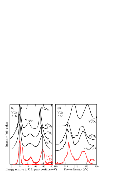
First, we discuss about the valence state of the V ions in IVO. Figure 1 shows the V core-level spectra of IVO and various vanadium oxides. The binding energy () of a core-level peak position is related to its charge state and, in general, becomes larger with increasing valency. In fact, it has been reported that the of the V peak increases with valency of V as shown in Fig. 1(a) PRB_79_Sawatzky . By comparing the peak position of the V core level of IVO with those of the other vanadium oxides, the valence state of V in In2O3 is found to be trivalent V3+ (). Figure 1(b) shows the V XAS spectra of IVO and several vanadium oxides. The line shape of the V spectrum of IVO is similar to that of V2O3 (V3+) DrThesis_Park rather than that of Zn1-xVxO (V2+) APL_07_Ishida and of V2O5 (V5+) JAP_07_Gloskovskii , consistent with the observation of the V XPS. The results suggest that the electronic structure of the doped V ion in IVO is close to that of the V ion in V2O3, i.e., V is in the trivalent V3+ state octahedrally coordinated by oxygens. Therefore, it is likely that the doped V ions are substituted for the In sites.
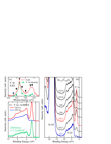
In order to obtain an understanding of the electronic structure of the V ion in the valence band, we measured V resonant photoemission spectra of IVO. Figure 2(b) shows the valence-band PES spectra of IVO taken at various photon energies in the V core-excitation region. Energy difference between the top of the O bands and is eV, comparable to the band gap of In2O3 eV, indicating that in the IVO sample is located near the bottom of the conduction band. We observed clear resonant enhancement in the valence band. The PES intensity as a function of photon energy (), i.e., constant-initial-state (CIS) spectrum, at eV demonstrates that the enhancement is proportional to the intensity of the V XAS as shown in Fig. 2(a). The on- and off-resonance spectra were chosen as measured at eV and 513 eV, respectively. The difference between the on- and off-resonance spectra yields the V PDOS. Although the relative intensities of different spectral features change with photon energy due to the effects of transition matrix elements and of the resonance, the structures (peak positions) of the V PDOS are independent of photon energy, implying that the V ions are in a single electronic state. The V PDOS shows a peak above the O band, that is, in the middle of the band gap of In2O3, as shown in Fig. 2(c). The narrow width and strong intensity of the peak imply the localized nature of the V orbitals in the valence band, i.e., weak mixing in IVO.
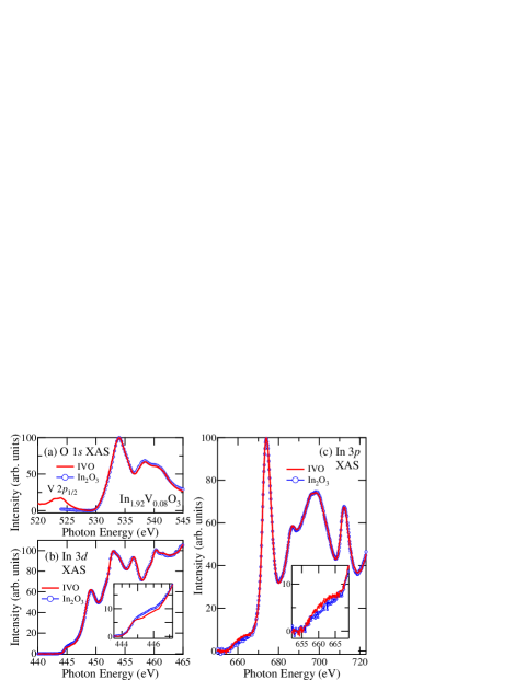
In -type DMS’s, electronic states near the bottom of the conduction band are expected to be important for carrier-induced ferromagnetism since is located there. Because the valence band of the host semiconductor is usually occupied, XAS spectra measured at the absorption edges of the host semiconductor reflect the unoccupied electronic states, namely, the conduction band, and are useful for the investigation of the electronic structure of -type DMS’s. Figure 3 shows XAS spectra measured at absorption edges of In and O, and compares them between V-doped and pure In2O3. The O XAS spectrum of IVO is nearly identical to that of In2O3 as shown in Fig. 3(a). It has been reported that the O XAS spectrum of Fe-doped In2O3 differs from that of pure In2O3, and that the difference is induced by hybridization of the Fe orbitals with the O band APL_07_Jayakumar . The observation implies weaker hybridization between the O band and the V orbitals in IVO than that between O and Fe in In2-xFexO3, consistent with the result of the V RPES. In contrast, the In and XAS spectra were changed by V doping, i.e., there are difference between the XAS spectra of IVO and these of pure In2O3 in both pre-edge regions as shown in Figs. 3(b) and 3(c). The observations clearly indicate hybridization between the In conduction band and the V orbitals in IVO.
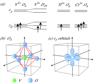
Based on the above findings, we shall discuss about the electronic structure of In2O3-based DMS’s, in particular, those doped with light-TM atoms. Electronic structure of a TM atom octahedrally coordinated by oxygens splits into two-fold degenerate and three-fold degenerate levels due to ligand crystal fields. In IVO, the V3+ () ion substituting for the In site has two electrons in the levels (or the two lowest levels splitted from the level due to the symmetry) as shown in Fig. 4(a). Because the orbitals are directed toward the O atoms as shown in Figs. 4(b) and 4(c), the O band can hybridize with the orbitals stronger than the orbitals. Indeed, the Slater-Koster parameter (), which represents transfer integrals between the and ligand orbitals, has an absolute value about twice larger than (), which represents transfer integrals between the and ligand orbitals Book_89_Harrison . Considering the result of O XAS, hybridization between the O band and the orbitals is expected to be weak. It is probable that the orbitals hybridize dominantly with the In band. Light TM ions Ti3+ and Cr3+ under the crystal field only have electron(s) in the levels, too [Fig. 4(a)]. It follows from those arguments that for light TM-doped In2O3, hybridization between the host conduction band and the orbitals should be taken into consideration to understand their electronic properties.
Considering the present observations, we shall discuss about the mechanism of the ferromagnetism in In2-xVxO. The bottom of the conduction band of In2O3 are mainly composed of the In bands PRB_97_Tanaka . For -type DMS’s, the electronic structure near the bottom of the conduction band is important, i.e., - exchange interaction may play an essential role rather than the - exchange interaction. It is possible that hybridization between the In and V orbitals as observed In XAS strengthens the - exchange interaction, as in the case of the host conduction band Co orbital exchange interaction in Ti1-xCoxO2 PRL_06_Quilty . Generally speaking, because in wide-gap semiconductors the effective mass is large, the magnetic splitting due to the exchange term in Hamiltonian (,- exchange interaction) is greater than the spin splitting of the host valence and conduction bands predicted by ordinary band theory, and the exchange contribution can be expressed as a large effective factor, which is given by
where is the band factor, is the factor of the ions, is the exchange constant, and is the Bohr magnetron, that is, for wide-gap semiconductors JAP_88_Furdyna . Therefore, the - exchange interaction accompanied by the spin splitting of the conduction band is expected to be dominant in In2-xVxO3. In such a case, magnetic circular dichroism signal at the optical absorption edge should be measurable. Additional measurements which are related to the spin splitting of the conduction band are highly desirable. Since the extent of orbitals diminish with increasing number of electrons, effects of cation- hybridization may weaken in heavy TM-doped DMS’s.
Assuming that light TM-doped In2O3 DMS’s have common properties, we can discuss about the role of oxygen vacancies in In2O3-based DMS’s. The oxygen vacancy is a major defect in oxides and acts as a double donor. In addition to electron doping by the vacancies, it has recently been proposed that the existence of oxygen vacancies themselves affects the ferromagnetic properties of oxide-based DMS’s through the formation of the donor-impurity band (in this case, the oxygen vacancies are the centers of bound magnetic polarons) NatMater_05_Coey , and reported that, even in non-magnetic oxide, the ferromagnetism can be induced by the oxygen vacancies PRB_06_Sundaresan ; MMM_07_Hong . For light TM-doped In2O3 DMS’s, there are several works related to oxygen vacancies. Philip et al. NatMater_06_Philip have reported that while Cr:In2O3 thin films deposited at high oxygen pressure (20 mTorr) show paramagnetic behavior, films deposited at low oxygen pressure (0.35 mTorr) exhibits ferromagnetic properties, where the low pressure growth induces in the thin films with electron carriers through the oxygen vacancies. Kharel et al. JAP_07_Kharel have found that while air annealed Cr-doped In2O3 film and bulk samples do not show ferromagnetism, samples annealed in a high vacuum are ferromagnetic due to the creation of oxygen vacancies. A first-principle electronic-structure calculation of In2O3 has predicted that when electrons are localized around the oxygen vacancy, the In-In bond is reinforced remarkably while the In-O bond is significantly weakened PRB_97_Tanaka . Considering this result together with the experimental findings, it is possible that, besides the electron carrier doping, the presence of oxygen vacancy augments the exchange interaction between the In conduction band and the orbitals. This effect may be stronger for light TM-doped In2O3 DMS’s than heavy TM-doped ones because of the shrinkage of the orbitals with the number of electrons. In order to set whether this consideration is valid or not, systematic measurements of In2O3-based DMS’s with independently controlled oxygen vacancies and carrier concentrations are desirable.
In conclusion, we have performed PES and XAS studies of In2-xVxO3 thin films in order to investigate their electronic structure and its relationship with ferromagnetism. From comparison with previous reports, the V ions are expected to be trivalent states, indicating that the V ion substitutes for the In site. The V PDOS in valence band has been observed using RPES technique and shows a sharp peak within the band gap of In2O3, implying the localized nature of the V orbitals in the valence band. There are differences of XAS spectra measured at In and edges although the O XAS spectrum is independent of V doping. Based on the findings, it is likely that the - exchange interaction is dominant for the ferromagnetism in In2-xVxO3. For light TM-doped In2O3, the role of oxygen vacancy has been discussed. The present results point to a need for taking into account hybridization between the host conduction band and orbitals in In2O3-based DMS’s, especially for light TM doped ones. We believe that the findings will promote further systematic studies of -type oxide-based DMS’s.
This work was supported by a Grant-in-Aid for Scientific Research in Priority Area “Spin Current: Its Creation and Control” (19048012) from MEXT, Japan. Work in Sweden is supported by the Swedish Agency VINNOVA, and the Carl Tryggers Stiftelse. MK and MT acknowledge support from the Japan Society for the Promotion of Science for Young Scientists.
References
- (1) H. Ohno, A. Shen, F. Matsukura, A. Oiwa, A. Endo, S. Katsumoto, and Y. Iye, Appl. Phys. Lett. 69, 363 (1996).
- (2) F. Matsukura, H. Ohno, A. Shen, and Y. Sugawara, Phys. Rev. B 57, R2037 (1998).
- (3) H. Ohno, Science 281, 951 (1998).
- (4) T. Dietl, H. Ohno, F. Matsukura, J. Cibert, and D. Ferrand, Science 287, 1019 (2000).
- (5) Y. Matsumoto, M. Murakami, T. Shono, T. Hasegawa, T. Fukumura, M. Kawasaki, P. Ahmet, T. Chikyow, S.-Y. Koshihara, and H. Koinuma, Science 291, 854 (2001).
- (6) S. B. Ogale, R. J. Choudhary, J. P. Buban, S. E. Lofland, S. R. Shinde, S. N. Kale, V. N. Kulkarni, J. Higgins, C. Lanci, J. R. Simpson, N. D. Browning, S. Das Sarma, H. D. Drew, R. L. Greene, and T. Venkatesan, Phys. Rev. Lett. 91, 077205 (2003).
- (7) P. Sharma, A. Gupta, K. V. Rao, F. J. Owens, R. Sharma, R. Ahuja, J. M. O. Guillen, B. Johnsson, and G. A. Gehring, Nat. Mater. 2, 673 (2003).
- (8) J. Philip, N. Theodoropoulou, G. Berera, J. S. Moodera, and B. Satpati, Appl. Phys. Lett. 85, 777 (2004).
- (9) Y. K. Yoo, Q. Xue, H.-C. Lee, S. Cheng, X.-D. Xiang, G. F. Dionne, S. Xu, J. He, Y. S. Chu, S. D. Preite, S. E. Lofland, and I. Takeuchi, Appl. Phys. Lett. 86, 042506 (2005).
- (10) N. H. Hong, J. Sakai, N. T. Huong, and V. Brizé, Appl. Phys. Lett. 87, 102505 (2005).
- (11) G. Peleckis, X. L. Wang, and S. X. Dou, Appl. Phys. Lett. 88, 132507 (2006).
- (12) N. H. Hong, J. Sakai, N. T. Huong, A. Ruyter, and V. Brizé, J. Phys.: Condens. Mat. 18, 6897 (2006).
- (13) G. Peleckis, X. Wang, and S. X. Dou, Appl. Phys. Lett. 89, 022501 (2006).
- (14) A. Gupta, H. T. Cao, K. Parekh, K. V. Rao, A. R. Raju, and U. V. Waghmare, J. Appl. Phys. 101, 09N513 (2007).
- (15) O. D. Jayakumar, I. K. Gopalakrishnan, S. K. Kulshreshtha, A. Gupta, K. V. Rao, D. V. Louzguine-Luzgin, A. Inoue, P.-A. Glans, J.-H. Guo, K. Samanta, M. K. Singh, and R. S. Katiyar, Appl. Phys. Lett. 91, 052504 (2007).
- (16) J. He, S. Xu, Y. K. Yoo, Q. Xue, H.-C. Lee, S. Cheng, X.-D. Xiang, G. F. Dionne, and I. Takeuchi, Appl. Phys. Lett. 86, 052503 (2005).
- (17) H. S. Kim, S. H. Ji, H. Kim, S.-K. Hong, D. Kim, Y. E. Ihm, and W. K. Choo, Solid State Commun. 137, 41 (2006).
- (18) J. Philip, A. Punnoose, B. I. Kim, K. M. Reddy, S. Layne, J. O. Holmes, B. Satpati, P. R. Leclair, T. S. Santos, and J. S. Moodera, Nat. Mater. 5, 298 (2006).
- (19) Z. G. Yu, J. He, S. Xu, Q. Xue, O. M. J. van’t Erve, B. T. Jonker, M. A. Marcus, Y. K. Yoo, S. Cheng, and X.-D. Xiang, Phys. Rev. B 74, 165321 (2006).
- (20) J. Stankiewicz, F. Villuendas, and J. Bartolomé, Phys. Rev. B 75, 235308 (2007).
- (21) I. Tanaka, M. Mizuno, and H. Adachi, Phys. Rev. B 56, 3536 (1997).
- (22) L. Marsella and V. Fiorentini, Phys. Rev. B 69, 172103 (2004).
- (23) H. Kim, C. M. Gilmore, A. Piqué, J. S. Horwitz, H. Mattoussi, H. Murata, Z. H. Kafafi, and D. B. Chrisey, J. Appl. Phys. 86, 6451 (1999).
- (24) C. G. Granqvist and A. Hultåker, Thin Solid Films 411, 1 (2002).
- (25) J. Okamoto, K. Mamiya, S.-I. Fujimori, T. Okane, Y. Saitoh, Y. Muramatsu, A. Fujimori, S. Ishikawa, and M. Takano, AIP Conf. Proc. 705, 1110 (2004).
- (26) Y. Saitoh, T. Nakatani, T. Matsushita, A. Agui, A. Yoshigoe, Y. Teraoka, and A. Yokoya, Nucl. Instrum. Methods Phys. Res. Sect. A 474, 253 (2001).
- (27) G. A. Sawatzky and D. Post, Phys. Rev. B 20, 1546 (1979).
- (28) J. Park, Thesis (University of Michigan, 1993).
- (29) Y. Ishida, J. I. Hwang, M. Kobayashi, Y. Takeda, K. Mamiya, J. Okamoto, S.-I. Fujimori, T. Okane, K. Terai, Y. Saitoh, Y. Muramatsu, A. Fujimori, A. Tanaka, H. Saeki, T. Kawai, and H. Tabata, Appl. Phys. Lett. 90, 022510 (2007).
- (30) A. Gloskovskii, S. A. Nepijko, G. Schönhense, H. A. Therese, A. Reiber, H. C. Kandpal, G. H. Fecher, C. Felser, W. Tremel, and M. Klimenkov, J. Appl. Phys. 101, 084301 (2007).
- (31) W. A. Harrison, Electronic Structure and the Properties of Solids (Dover, New York, 1989).
- (32) J. W. Quilty, A. Shibata, J.-Y. Son, K. Takubo, T. Mizokawa, H. Toyosaki, T. Fukumura, and M. Kawasaki, Phys. Rev. Lett. 96, 027202 (2006).
- (33) J. K. Furdyna, J. Appl. Phys. 64, R29 (1988).
- (34) J. M. D. Coey, M. Venkatesan, and C. B. Fitzgerald, Nat. Mater. 4, 173 (2005).
- (35) A. Sundaresan, R. Bhargavi, N. Rangarajan, U. Siddesh, and C. N. R. Rao, Phys. Rev. B 74, 161306(R) (2006).
- (36) N. H. Hong, J. Sakai, and F. Gervais, J. Magn. Magn. Mater. 316, 214 (2007).
- (37) P. Kharel, C. Sudakar, M. B. Sahana, G. Lawes, R. Suryanarayanan, R. Naik, and V. M. Naik, J. Appl. Phys. 101, 09H117 (2007).