Graphene Antidot Lattices – Designed Defects and Spin Qubits
Abstract
Antidot lattices, defined on a two-dimensional electron gas at a semiconductor heterostructure, are a well-studied class of man-made structures with intriguing physical properties. We point out that a closely related system, graphene sheets with regularly spaced holes (“antidots”), should display similar phenomenology, but within a much more favorable energy scale, a consequence of the Dirac fermion nature of the states around the Fermi level. Further, by leaving out some of the holes one can create defect states, or pairs of coupled defect states, which can function as hosts for electron spin qubits. We present a detailed study of the energetics of periodic graphene antidot lattices, analyze the level structure of a single defect, calculate the exchange coupling between a pair of spin qubits, and identify possible avenues for further developments.
pacs:
73.21.La, 73.20.At, 03.67.LxGraphene is the rapidly rising star of low-dimensional materials. Following the initial reports on fabrication by mechanical peeling Novoselov et al. (2004) and epitaxial growth Berger et al. (2004), this exceptional material has stimulated considerable experimental Geim and Novoselov (2007) and theoretical research Katsnelson et al. (2006) as well as proposals for novel electronic devices Rycerz et al. (2007). The promising prospects for graphene devices are based on several remarkable properties. Mainly, the sample quality and mobility (exceeding 15000 cm2/Vs Geim and Novoselov (2007)) can be very high. In addition, patterning of such monolayer films by e-beam lithography Geim and Novoselov (2007); Berger et al. (2006) with features as small as 10 nm Geim and Novoselov (2007); Han et al. (2007) is possible. Very recently, spintronics devices have been considered Hill et al. (2006). The incentive for graphene based spintronics lies partly in the long spin coherence time that is characteristic of carbon-based materials. This also has obvious advantages within the field of solid-state quantum information processing, where confined electron spins have been promoted as carriers of quantum information Loss and DiVincenzo (1998). Being a light element, carbon has a rather small spin-orbit coupling, and, moreover, the predominant 12C isotope has a vanishing hyperfine interaction. This makes graphene, at least in principle, a superior material compared to existing quantum computing implementations in GaAs Trauzettel et al. (2007); Petta et al. (2005).
Antidot lattices, defined on semiconductor heterostructures, display many intricate transport properties, in particular in magnetic fields where the competing length scales lead to rich physics Weiss et al. (1991). In this Letter we wish to draw attention to the possibility of forming antidot lattices on graphene. As mentioned above, state-of-the-art e-beam lithography has been used to carve graphene nanoribbons with feature sizes down to tens of nanometers. We propose to use similar techniques to create regular holes in the graphene sheet, in order to form antidot lattices. The antidot lattice has the important consequence that it turns the semi-metallic graphene into a gapped semiconductor, where the size of the gap can be tuned via the antidot lattice parameters. As our analysis shall show, this electronic structure can be manipulated further so as to create coupled electron spin qubits, thus suggesting that these perforated graphene sheets are a promising platform for a large-scale spin qubit architecture. Localized spin qubit states can be formed in the antidot lattice by deliberately omitting some of the antidots. This idea has previously been analyzed for the two-dimensional electron gas in e.g. GaAs heterostructures Flindt et al. (2005). As we will now argue, moving to graphene has three major advantages: (i) increased coherence time; (ii) favorable energy scale of the defect states; and (iii) increased lateral confinement.
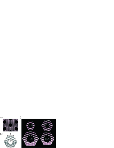
The proposed antidot lattice is simply a triangular array of holes in a graphene sheet, as illustrated in Fig. 1a. The lattice consists of hexagonal unit cells as shown in Fig. 1b, in which a roughly circular hole is created. We characterize the structure by the side length of the hexagonal unit cell and the radius of the hole, both measured in units of the graphene lattice constant Å. A lattice is designated by the notation . Note that while is an integer, can be non-integer. As is evident from the examples in Fig. 1c, is equal to the number of carbon atoms in the outermost row of the hexagon. Also of importance are the total number of sites in the unit cell (equal to the number of atoms before the hole is made) and the number of removed atoms . As an example, for the lattice = 294 and . Below, results for structures with and varying have been compiled taking care that no dangling bonds are formed, i.e. that all atoms have at least two neighbors. While these structures are too small for present-day lithography, results for realistic structures are easily obtained by simple scaling laws, as demonstrated below.
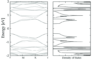
We model the structures using a tight-binding (TB) description considering a single -orbital on each site and assuming a nearest-neighbor hopping integral of , with eV Saito et al. (1998). In this description, energy levels are always distributed symmetrically above and below zero, which defines the Fermi level in the undoped case. The TB approximation is necessary due to the large antidot cells. It is known to accurately reproduce the low-energy part of the density-functional (DFT) band structure of graphene Reich et al. (2002b). Edges, however, require a modification of hopping integrals near the edge to ensure agreement between DFT and TB calculations Son et al. (2006b). We have checked that the computed band structures are generally robust against such modifications, which simply produce a minor additional opening of the band gap. The electronic band structure and density of states for the structure are illustrated in Fig. 2. Importantly, a substantial energy gap of approximately 0.73 eV opens around the Fermi level rem . Hence, as hinted above, the periodic perturbation turns the semi-metal into a semiconductor. In the top panel of Fig. 3, band gaps of several structures are plotted versus the quantity . When plotted in this manner, a roughly linear behavior is observed. This simple result may be rationalized within the linearized Hamiltonian approximation treating electrons as massless Dirac fermions subject to the periodic perturbation of the antidot lattice. In this description, the wave function is a two-component spinor representing the two sublattices. The corresponding Hamiltonian is the matrix operator
| (1) |
where is the periodic antidot potential, is the momentum operator, and the Fermi velocity m/s. In the absence of a potential, the energy eigenvalues are simply . If the potential is approximated by infinite barriers at the positions of the antidots, the eigenvalue problem is reduced to the form
| (2) |
with the boundary condition that vanishes in the barrier region. The equation is mathematically similar to the usual effective mass equation. For an antidot lattice in a usual semiconductor material such as GaAs, simple scaling arguments lead to a band gap varying as , where is the area of the unit cell and is the area removed inside each unit cell. In graphene, a similar behavior is expected except that the linear band structure changes the prefactor from to , i.e. . The fit in Fig. 3 shows that approximately follows a square root behavior . Thus, the net result is a gap varying as with a constant eV. For large unit cells, is small and in this case the linear fit is an excellent approximation. The weaker scaling ( instead of ) of graphene is very favorable for the purpose of obtaining large band gaps even for relatively large structures. The practical limits of present day e-beam lithography probably restrict the obtainable size of the unit cell to around 10 nm across corresponding to a total number of carbon atoms of . Assuming we find a substantial gap of 0.23 eV. Hence, band gaps much larger than the thermal energy at room temperature are certainly realistic. This feature, which is a direct consequence of the massless Dirac fermion behavior, is very important for the feasibility of the graphene based devices considered here.
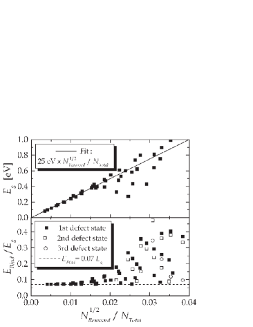
We now turn to the role of intentional defects in the antidot lattice produced by leaving one or several unit cells intact, i.e. without a hole. Such defects may support localized electronic states and may consequently be utilized for electron spin qubits, as we will now demonstrate. An example of single and double defects for the structure is shown in Fig. 4. For isolated single defects, we compute localized states by periodically replicating the super cell consisting of one intact and six perforated cells illustrated in the figure. The states are sufficiently localized that cross-talk between neighboring super cells is negligible. Periodicity is not crucial for the appearance of bound states Flindt et al. (2005). Defect states are identified by an energy lying in the fundamental energy gap, i.e. the gap containing the Fermi energy. In fact, other energy gaps may exist as illustrated in Fig. 2; here we focus solely on states in the fundamental gap. If the gap is sufficiently large (i.e. if is large) several defect states are supported. In the lower panel of Fig. 3, a compilation of binding energies for the three lowest defect states is shown. We define the binding energy as the downwards shift of the defect state energy measured from the conduction band edge. Hence, a defect state at the Fermi energy would have a binding energy of . For small band gaps, only a single defect state is supported but several defect states appear in an irregular pattern as the confinement increases. Note that the scatter in the data points in the plot reflects actual variations and not computational inaccuracy. Importantly, the binding energy in the limit of small band gaps is seen to approach a constant fraction of the energy gap. Hence, for the 10 nm unit cell considered above, a defect state would be bound by roughly 16 meV. This implies that liquid nitrogen cooling should be sufficient to observe these states.
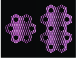
Next, we consider two tunnel coupled defect states in a “double defect”, illustrated in Fig. 4. With an electron occupying a non-degenerate state in each defect, the spins of the two electrons couple due to the exchange interaction . If the two single-defect states are energetically aligned, the exchange coupling is given as according to the Hubbard approximation. Here, is the tunnel coupling between the two defect states, and is the single-defect Coulomb energy. As discussed in Ref. Loss and DiVincenzo (1998), the exchange coupling constitutes a key element in quantum computing architectures based on electron spins as qubits, enabling interactions between different qubits. Importantly, the exchange coupling can be controlled with external gate potentials. Metallic gates could be realized by lithographic methods and placed either below or on top of the graphene sheet but will not be considered further here. For evaluation of the exchange coupling, we calculate the single-defect Coulomb energy by the method presented in Ref. Pedersen, 2004 (ignoring overlap between different atomic -orbitals) using the Ohno form to interpolate between the intra- and long-range inter-atomic Coulomb coupling. A Hubbard for carbon -orbitals of 20.08 eV Pedersen (2004) and dielectric constant of 2.5 Ando (2006) (as appropriate for graphene on SiO2) are applied. The tunnel coupling is extracted from the single-particle energy spectrum.
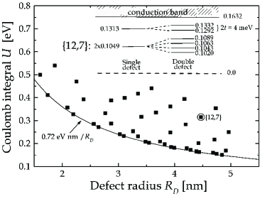
Our findings for the Coulomb energy are illustrated in Fig. 5. In the plot, is the effective defect radius calculated by including half the area of the surrounding cells and writing the total area as . The smallest ’s are found for the least localized states for which scales as the expected . The inset shows, as an example, the single-electron level diagram for single- and double defects in a lattice. This structure has = 864 and and supports two single-defect states. Of these, the upper one is non-degenerate and the Coulomb energy is 0.315 eV. Due to the large double defect super cell, this is about the largest structure that we have been able to analyze. As shown, the level splitting corresponds to a tunnel coupling of meV between the two non-degenerate single-defect states. Hence, based on the values we may estimate the exchange coupling to be on the order of eV. Naturally, this value could be tuned by appropriate design of the barrier region that, for simplicity, has been constructed from two intact unit cells. Also, going to larger single defects would decrease and, in turn, increase . Note, however, that depends exponentially on barrier width whereas is only weakly dependent on geometry. Hence, the geometric influence on will be determined mainly through rather than .
We believe that the approach outlined above can be extended to more complicated structures. Going from a single pair of spin qubits in an isolated double defect to several coupled spins could be achieved with little added complication. Similarly, a double defect could be replaced by a linear array of defects. Hence, the number of qubits can be increased essentially without complicating the fabrication procedure. In practice, excellent control of the e-beam lithography process remains a critical issue.
In summary, we have shown that antidot lattices pave the way for controlled manipulation of the electronic properties of graphene sheets. The material can be rendered semiconducting with a significant and controllable energy gap. The magnitude of the gap is explained by a simple scaling argument and could reach several tenths of eVs for realistic structures. Introducing defects into the antidot lattice leads to the formation of localized electronic states. Combined with the extremely long spin coherence time of carbon-based materials this could lead to a practical realization of spin qubits. With a properly designed double defect, two-electron states derived from defect levels near the Fermi level are found to fulfil the requirements for such qubits.
Acknowledgements.
APJ and CF acknowledge the FiDiPro program of the Finnish Academy of Sciences for support during the final stages of this work. We thank Dr. A. Krasheninnikov for an informative discussion on gap states in graphene.References
- Novoselov et al. (2004) K. S. Novoselov et al., Science 306, 666 (2004).
- Berger et al. (2004) C. Berger et al., J. Chem. Phys. B 108, 19912 (2004).
- Geim and Novoselov (2007) A. K. Geim and K. S. Novoselov, Nature Mat. 6, 183 (2007).
- Katsnelson et al. (2006) M. I. Katsnelson, K. S. Novoselov, and A. K. Geim, Nature Phys. 2, 620 (2006), V. V. Cheianov, V. Fal’ko, and B. L. Altshuler, Science 315, 1252 (2007).
- Rycerz et al. (2007) A. Rycerz, J. Tworzydlo, and C. W. J. Beenakker, Nature Phys. 3, 172 (2007).
- Berger et al. (2006) C. Berger et al., Science 312, 1191 (2006).
- Han et al. (2007) M. Y. Han, B. Özyilmaz, Y. Zhang, and P. Kim, Phys. Rev. Lett 98, 206805 (2007).
- Hill et al. (2006) E. W. Hill et al., IEEE Trans. Magn. 42, 2694 (2006), Y. Son, M. L. Cohen, and S. G. Louie, Nature 444, 347 (2006a), T. B. Martins, R. H. Miwa, A. J. R. da Silva, and A. Fazzio, Phys. Rev. Lett 98, 196803 (2007).
- Loss and DiVincenzo (1998) D. Loss and D. P. DiVincenzo, Phys. Rev. A 57, 120 (1998), G. Burkard, D. Loss, and D. P. DiVincenzo, Phys. Rev. B 59, 2070 (1999), D. P. DiVincenzo et al., Nature 408, 339 (2000).
- Trauzettel et al. (2007) B. Trauzettel, D. V. Bulaev, D. Loss, and G. Burkard, Nature Phys. 3, 192 (2007).
- Petta et al. (2005) J. R. Petta et al, Science 309, 2180 (2005).
- Weiss et al. (1991) D. Weiss et al., Phys. Rev. Lett. 66, 2790 (1991).
- Flindt et al. (2005) C. Flindt, N. A. Mortensen, and A. P. Jauho, Nano Lett. 5, 2515 (2005), J. Pedersen, C. Flindt, N. A. Mortensen, and A. P. Jauho, arXiv:0801.1005v1, to appear in Phys. Rev. B (2008).
- Saito et al. (1998) R. Saito, G. Dresselhaus, and M. S. Dresselhaus, Physical Properties of Carbon Nanotubes (Imperial College Press, 1998).
- Reich et al. (2002b) S. Reich, J. Maultzsch, C. Thomsen, and P. Ordejón, Phys. Rev. B. 66, 35412 (2002b).
- Son et al. (2006b) Y. Son, M. L. Cohen, and S. G. Louie, Phys. Rev. Lett. 97, 216803 (2006b).
- (17) This prediction is unchanged, if one modifies the tight-binding parameters along the edges of the perforation, as suggested in Ref. Son et al., 2006b. Also, perfect periodicty of the holes is not crucial as discussed in Ref. Flindt et al. (2005).
- Pedersen (2004) T. G. Pedersen, Phys. Rev. B 69, 75207 (2004).
- Ando (2006) T. Ando, J. Phys. Soc. Jpn. 75, 74716 (2006).