Gap opening with ordering in PrFe4P12 studied by local tunneling spectroscopy
Abstract
We present measurements of the local tunneling density of states in the low temperature ordered state of PrFe4P12. The temperature dependencies of the Fermi level density of states, and of the integrated density of states at low bias voltages, show anomalies at , the onset of multipolar ordering as detected by specific heat and other macroscopic measurements. In the ordered phase, we find a local density of states with a V-shape form, indicating partial gap opening over the Fermi surface. The size of the gap according to the tunneling spectra is about 2 meV.
pacs:
71.27. a+,71.30 +h, 73.20.-rRecently, a new family of heavy fermion f-electron intermetallic compounds with the filled skutterudite structure RT4X12 (R is a rare earth, T a transition metal and X a pnictogen) has been found to show many attractive phenomena, most of them appearing at low temperatures. Among others, metal-insulator transition, heavy fermion behavior, and superconductivity have been found in (R=Pr) systemsAoki et al. (2005); Bauer et al. (2002); Sekine et al. (1997); Measson et al. (2004); Suderow et al. (2004); Sugawara and et al. (2002).
In particular, in PrFe4P12, a peculiar phase transition occurs at TA = 6.5 K, with distinct anomalies in both resistivitySato et al. (2000) and specific heatAoki et al. (2002). The intriguing order below TA is widely believed to be associated with orbital degrees of freedomAoki et al. (2005). A recent NMR studyKikuchi et al. (2007) has put severe restrictions on the symmetry of the order parameter. According to it, the ordering involves non-magnetic multipoles, which do not break the point symmetry of the crystal at the Pr sites. The scalar order with Kiss and Kuramoto (2006) is currently the most promising candidate to represent the order parameter. On the other hand, according to transport studiesSato et al. (2000); Sugawara and et al. (2002); Pourret and et al. (2006), the itinerant electrons are profoundly affected by this phase transition. The multifold increase in the Hall, Seebeck and Nernst coefficients all suggest a drastic decrease in the number of charge carriersPourret and et al. (2006). This is compatible with the results of a de Haas van Alphen studySugawara and et al. (2002), which found a small Fermi surface (0.0015 of the Brillouin zone) with a moderate effective mass (10me) in the ordered state. In higher magnetic fields (strong enough to destroy the ordering), the same study resolved several larger Fermi surfaces with heavier masses up to 81me Sugawara and et al. (2002). The consequences of the ordering on transport properties recall the case of URu2Si2Behnia et al. (2005). In both cases, the ordering leads to an enhanced lattice thermal conductivity, a large Hall coefficient and anomalously large Nernst and Seebeck coefficients due to an incomplete metal-insulator transition, producing a heavy-Fermion semi-metal. In the case of URu2Si2, a partial gap opening has been observed using different techniquesFlouquet (2005); Naidyuky and Yanson (1998).
On the other hand, scanning tunneling microscopy and spectroscopy (STM/S) techniques have been widely applied to systems where some kind of energy gap appears in the quasiparticle spectrum. The superconducting gap is certainly one of the most studied kinds of energy gaps viewed using this technique, although different kinds of charge ordered, and semimetallic or semiconducting compounds, have also received attentionFischer et al. (2007); Hofer et al. (2003). Any features in the density of states at energies of the order of the meV are relatively easy to resolve using STM/S, because the tip density of states remains featureless and temperature independent below several tens of meV. Therefore, when a tip is scanned over a surface, the bias dependence of the local tunneling conductance, below some tens of mV, is simply the temperature smeared local density of states of the sample. Examples of STM/S experiments showing a temperature dependent gapped density of states include e.g. the intriguing pseudogap of the High Tc superconductors, the charge density wave gap in the di-chalchogenides, or the peculiar low energy electronic features appearing in graphite Fischer et al. (2007); Coleman et al. (1988); Matsui et al. (2005). Here we present local tunneling conductance measurements at low temperatures made with STM/S that evidence the appearance of a gap in the quasiparticle spectrum of the heavy fermion material PrFe4P12.
We use a home built STM/S system in a 4He refrigerator that goes down to 1.5 K, and has been used for several previous work in superconducting materialsSuderow et al. (2001); Rubio-Bollinger et al. (2001); Rodrigo et al. (2004). The STM/S has a scanning range of about 2 x 2 m at low temperatures, and a sample holder that allows to move in-situ the tip over the whole area of the sample. When needed, the tip is prepared and cleaned in-situ following the methods discussed in Refs.Rodrigo et al. (2004); Guillamon et al. (2007). We took a small single crystalline sample broken at ambient conditions and mounted into the STM sample holder, and used tips of Au. The tip tunnels into the (100) direction of the single crystalline sample. The sample showed large surface areas where clean tunneling conditions could be achieved, with tunneling conductance curves that were reproducible over the whole surface. Moreover, the current-distance characteristics signalled work functions of several eV, and the topography and spectroscopy was independent of the tunneling resistance.
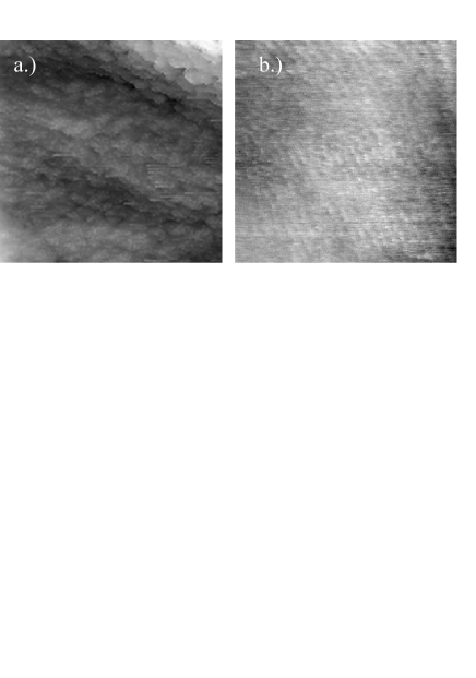
Typical images (Figs.1) consist of irregular terraces or small nanoscopic size granular structures, very similar to the ones observed on the surface of several superconducting materials Suderow et al. (2001); Rubio-Bollinger et al. (2001); Suderow et al. (2004). In some surface regions, we could observe regular terraces with characteristic distances of the order of the unit cell (Fig.1b). Over the whole surface, we reproducibly observe a gapped local density of states. The curves shown in Fig.2 are obtained in large images of the surface, above and below the ordering temperatures. Above TA, the tunneling conductance shows no significant temperature dependence, besides temperature smearing. The curves are usually slightly parabolic, with a density of states, which has a small bias dependence around the Fermi level. Typically, in this voltage range, metals show a flat density of states. Here, the small decrease of the density of states may signal a band structure with a peculiar form at energies very close to the Fermi level, that may preclude the opening of the gap in the ordered phase. When ordering sets in, a new energy scale appears in the tunneling conductance curves, which show a steep decrease for voltages below about 2 mV. At the lowest temperatures (1.5 K), the decrease is sharpest. The local density of states shows then closely a linear behavior at very low energies, with a characteristic V shape and a density of states at the Fermi level that remains relatively high.
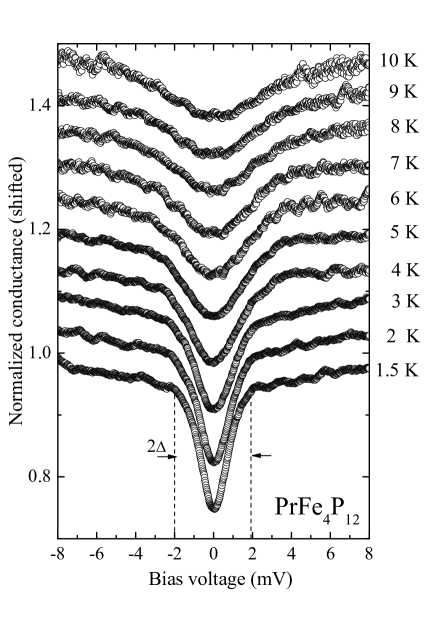
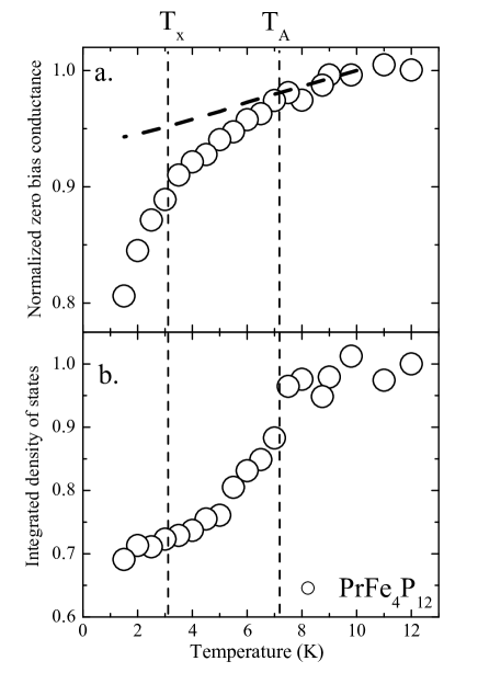
Note that the decrease is not a simple consequence of the reduced temperature smearing of the data above TA. To see this, we have plotted as the dashed line in Fig.3a the zero bias conductance calculated by reducing temperature smearing from the tunneling conductance above TA, and normalized the result to one at 10 K. The expected variation is smooth. However, the experimental data (circles in Fig.3a) show a steep decrease which sets in at TA and becomes more pronounced below Tx. The latter temperature scale (T) is associated with features in the transport data (most visible in the Hall mobility and the Nernst coefficientPourret and et al. (2006)). These two characteristic temperatures are recovered as kinks in the temperature dependence of the zero bias conductance. When extrapolating these data to zero temperature, we find that the local Fermi level density of states is about 30% smaller than in the high temperature phase. Furthermore, the integral over the local density of states measured at low energies (Fig.3b) also changes strongly below TA. Indeed, the integral of tunneling conductance curves obtained from a temperature independent density of states also remains temperature independent. Here we observe instead a strong drop below TA, evidencing the loss of charge carriers associated with the ordered state. Actually, the integral rapidly falls down to about 70% its value in the high temperature phase, and remains roughly constant, even on crossing the transition Tx. So below Tx, the decrease of the local Fermi level density of states (Fig.3a), is compensated by a slight increase at the shoulders of the conductance curves around 2mV.
The gap edge can be obtained from the voltage position of the onset of the decrease of the tunneling conductance curves down to the V shape observed at low temperatures (dashed lines in Fig.2). We find = 2 meV, which gives about 2/kBTA7, a value that is significantly larger than the mean field BCS result (2/kBTA = 3.7) previously used in the discussion of charge or spin density wave phenomenaColeman et al. (1988); Dai et al. (1993); Kiss et al. (2007).
On the other hand, the origin of the V-shape density of states and the significance of the high density of states obtained at the Fermi level and at low temperatures have to be discussed more carefully. As it is well known, in a local tunneling spectroscopy experiment, the obtained local density of states is formed by contributions coming from very different parts of the Fermi surfaceFischer et al. (2007). There is no selectivity in the direction perpendicular to the surface of the sample, as in a planar junction, and, in principle, many in-plane and out of plane momenta are probedFischer et al. (2007); Hofer et al. (2003). However, precise information of the actual electrons taking part in the tunneling process is very difficult to obtain without atomic resolution and comparison with theoretical calculationsGuillamon et al. (2007). For instance, note that in the well studied superconducting material MgB2, where until now no STM/S experiment has been made with atomic resolution, nearly all STM/S data show the opening of the superconducting gap on only part of the Fermi surface, namely the so called band gapRubio-Bollinger et al. (2001). Data from the rest of the Fermi surface, the so called bands, where the electron phonon coupling is larger, are more difficult to obtain using STM/S. Actually, STM/S experiments in this compound have never unambiguously shown tunneling features close to what one would expect taking into account the opening of the gap over the whole Fermi surfaceSuderow et al. (2002); Eskildsen et al. (2003); comprehensive review of the properties of MgB2 can be found in the volume (2003). In general, it is reasonable to assume that lighter electrons couple better with the states of the tip, so that local tunneling may preferentially reflect the properties of the Fermi surface with less mass renormalization, as possibly occurs in MgB2.
In the case of PrFe4P12, the magnitude of decrease in the conductance integral indicates that about one third of the electrons participating in the tunneling process come from the gapped part of the Fermi surface. The rest, i.e. the vast majority, must come from part of the Fermi surface where there is no gap at all, or it is vanishingly small. The de Haas van Alphen dataSugawara and et al. (2002) have detected a small and almost spherical Fermi surface in the center of the Brillouin zone. The size of this Fermi surface is in very good agreement with the carrier density extracted from the low-temperature positive Hall coefficient. Therefore, it is reasonable to assume that this is a hole-like band with a large electronic mobility dominating the Hall response of the system. However, other Fermi surfaces, electron-like, with a larger mass and a lower mobility may have remained undetected by dHvA. They would account for the relatively large magnitude of the linear specific heatSugawara and et al. (2002) and thermopowerPourret and et al. (2006). According to band structure calculationsHarima and Takegahara (2002), in addition to a small hole-like spherical surface at the -point, there is a large quasi-cubic Fermi surface subject to strong a nesting instability. Nesting would lead to a quasi-complete destruction of this larger Fermi surface, leading to small surviving portions (with unknown shape and energy dispersion) coexisting with the small spherical Fermi surface at the center of the Brillouin zone.
Thus, it is tempting to assume that local tunneling spectroscopy experiments preferentially probe the small Fermi surface barely affected by the ordering. The large Fermi level conductance found at low temperatures may result from this Fermi surface. On the other hand, the opening of the gap and the V-shape structure of the curves, may be a signature of the other (that is the larger, nested and undetected) Fermi surface. This would explain the non-observation of a fully developed gap in our experiments, as may be naively expected taking into account the reduction of charge carriers in the ordered phase observed in other experimentsSugawara and et al. (2002); Pourret and et al. (2006), and would be also compatible with the nesting scenario.
We note also that the temperature dependence of the local tunneling conductance shown in Fig.3 suggests that the behavior observed here is generated by the bulk and is not merely a surface property. Nevertheless, as in all STM/S experiments, surface related effects could in principle influence some of the features of the spectra, as their precise form or voltage dependence.
In summary, we have detected the consequences of the ordering on local tunneling spectroscopy. The temperature dependence of the tunneling spectra coincides with bulk results. Thus, the measured tunneling density of states reproduces the behavior found in part of the Fermi surface. In particular, we find a gap is of 2 meV, which gives 2 7, and that there are still parts of the Fermi surface that remain ungapped. This shows that the peculiar ordering in this compound leads to a largely frustrated metal insulator transition, and shapes the electronic band structure in such a way as to produce further peculiar properties.
I Acknowledgments.
We acknowledge discussions with J. Flouquet and J.P. Brison, and support from COST P-16 and from NES. The Laboratorio de Bajas Temperaturas is associated to the ICMM of the CSIC. This work was supported by the spanish MEC (Consolider Ingenio 2010 and grant FIS-2004-02897), and by the Comunidad de Madrid through program ”Science and technology at the millikelvin” (S-0505/ESP/0337).
References
- Aoki et al. (2005) Y. Aoki, H. Sugawara, H. Harima, and H. Sato, Journal of the Physical Society of Japan 74, 209 (2005).
- Bauer et al. (2002) E. Bauer, N. A. Frederick, P.-C. Ho, V. S. Zapf, and M. B. Maple, Phys. Rev. B 65, 100506(R) (2002).
- Sekine et al. (1997) C. Sekine, T. Uchiumi, I. Shirotani, and T. Yagi, Phys. Rev. Lett 79, 3218 (1997).
- Measson et al. (2004) M. A. Measson, D. Braithwaite, J. Flouquet, G. Seyfarth, J. P. Brison, E. Lhotel, C. Paulsen, H. Sugawara, and H. Sato, Phys. Rev. B 70, 64516 (2004).
- Suderow et al. (2004) H. Suderow, S. Vieira, J. D. Strand, S. Bud’ko, and P. C. Canfield, Phys. Rev. B 69, 060504(R) (2004).
- Sugawara and et al. (2002) H. Sugawara and et al., Phys. Rev. B 66, 134411 (2002).
- Sato et al. (2000) H. Sato, Y. Abe, H. Okada, T. D. Matsuda, K. Abe, H. Sugawara, and Y. Aoki, Phys. Rev. B 62, 15125 (2000).
- Aoki et al. (2002) Y. Aoki, T. Namiki, T. D. Matsuda, K. Abe, H. Sugawara, and H. Sato, Phys. Rev. B 65, 064446 (2002).
- Kikuchi et al. (2007) J. Kikuchi, M. Takigawa, H. Sugawara, and H. Sato, J. Phys. Soc. Japan 76, 024710 (2007).
- Kiss and Kuramoto (2006) A. Kiss and Y. Kuramoto, J. Phys. Soc. Japan 75, 103704 (2006).
- Pourret and et al. (2006) A. Pourret and et al., Phys. Rev. Lett. 96, 176402 (2006).
- Behnia et al. (2005) K. Behnia, R. Bel, Y. Kasahara, Y. Nakajima, H. Jin, H. Aubin, K. Izawa, Y. Matsuda, J. Flouquet, Y. Haga, et al., Phys. Rev. Lett. 94, 156405 (2005).
- Flouquet (2005) J. Flouquet, Progress in Low Temperature Physics XV, Elsevier (2005).
- Naidyuky and Yanson (1998) Y. G. Naidyuky and I. K. Yanson, J. Phys. Cond. Matt. 10, 8905 (1998).
- Fischer et al. (2007) O. Fischer, M. Kugler, I. Maggio-Aprile, and C. Berthod, Review of Modern Physics 79, 353 (2007).
- Hofer et al. (2003) W. A. Hofer, A. S. Foster, and A. L. Shluger, Rev. Mod. Phys. 75, 1287 (2003).
- Coleman et al. (1988) R. V. Coleman, B. Giambattista, P. K. Hansma, A. Johnson, W. W. McNairy, and C. G. Slough, Advances in Physics 37, 559 (1988).
- Matsui et al. (2005) T. Matsui, H. Kambara, Y. Niimi, K. Tagami, M. Tsukada, and H. Fukuyama, Phys. Rev. Lett. 94, 226403 (2005).
- Suderow et al. (2001) H. Suderow, P. Mart nez-Samper, S. Vieira, N. Luchier, J. P. Brison, and P. C. Canfield, Phys. Rev. B 64, 020503(R) (2001).
- Rubio-Bollinger et al. (2001) G. Rubio-Bollinger, H. Suderow, and S. Vieira, Phys. Rev. Lett. 86, 5582 (2001).
- Rodrigo et al. (2004) J. Rodrigo, H. Suderow, S. Vieira, E. Bascones, and F. Guinea, J. Phys.: Condens. Matter 16, 1151 (2004).
- Guillamon et al. (2007) I. Guillamon, H. Suderow, F. Guinea, and S. Vieira, Phys. Rev. B 77, 134505 (2007).
- Dai et al. (1993) Z. Dai, Q. Xue, Y. Gong, C.G. Slough, R.V. Coleman, Phys. Rev. B 48, 14543 (1993).
- Kiss et al. (2007) T. Kiss, T. Yokoya, A. Chainani, S. Shin, T. Hanaguri, M. Nohara, and H. Takagi, Nature Physics 3 p. (2007).
- Suderow et al. (2002) H. Suderow, M. Crespo, P. Martínez-Samper, J. Rodrigo, G. Rubio-Bollinger, S. Vieira, N. Luchier, J. P. Brison, and P. C. Canfield, Physica C 369, 106 (2002).
- Eskildsen et al. (2003) M. R. Eskildsen, N. Jenkins, G. Levy, M. Kugler, . Fischer, J. Jun, S. M. Kazakov, and J. Karpinski, Phys. Rev. B 68, 100508(R) (2003).
- comprehensive review of the properties of MgB2 can be found in the volume (2003) A. comprehensive review of the properties of MgB2 can be found in the volume, Physica C 385, 1 (2003).
- Harima and Takegahara (2002) H. Harima and K. Takegahara, Physica B 312-313, 843 (2002).