Kondo resonance in an ac driven quantum dot subjected to finite bias
Abstract
We employ the time-dependent non-crossing approximation to study the time averaged conductance for a single electron transistor in the Kondo regime when the dot level is sinusoidally driven from its equilibrium position by means of a gate voltage in finite bias. We find that the average conductance exhibits significant deviation from the monotonous reduction when the applied bias is equal to the driving frequency of the dot level. We investigate the effect of the temperature and the driving frequency on the observed enhancement. We attribute this behaviour to the overlap of the satellite Kondo peaks with the split Kondo resonances formed at each lead’s Fermi level. We display the spectral function to put our interpretation into more rigorous footing.
pacs:
72.15.Qm, 85.35.-pThe advent of the state-of-the-art nanotechnology experiments provided unprecedented control over nanostructures like quantum dots which enabled to test various theoretical predictions. One of these predictions was a long standing question on whether the Kondo effect, which is a hallmark of condensed matter physics, would dominate the low temperature transport through a quantum dot NgLee88PRL ; GlazmanRaikh88JL . Subsequent experiments resolved this controversy by confirming these predictions GoldhaberetAl98Nature ; GoldhaberetAl98PRL ; CronenwettetAl98Science .
The Kondo effect derives its name from the seminal work of Jun Kondo Kondo64PTP in which he discovered that bulk metals with magnetic impurities providing localized unpaired spins would experience an enhancement in their resistivities at low temperatures due to the formation of a spin singlet resulting from the interaction of the unpaired localized electron and delocalized electrons near the Fermi level KouwenhovenGlazman01PW . The requirement to obtain the Kondo effect in quantum dots is to confine odd number of electrons in the dot. This results in a net spin in the dot and a new transport channel opens when this net spin is coupled to the fermionic bath in the metallic leads giving rise to a peak at the Fermi level in the dot density of states. Ambient temperature, bias and magnetic field greatly influence the sharpness of this peak
The effects of abrupt perturbations by step-like switching of the gate or source-drain voltage have been investigated extensively NordlanderetAl99PRL ; PlihaletAl00PRB ; SchillerHershfield00PRB ; MerinoMarston04PRB and they unambiguously demonstrated that the resulting transient current exhibits three different time scales PlihaletAl05PRB ; AndersSchiller05PRL ; AndersetAl06PRB ; IzmaylovetAl06JPCM . The initial fast non-Kondo timescale is characterized by the reshaping of the Fano resonance while the Kondo resonance reaches a metastable state at the end of the much longer Kondo timescale. A third and longest timescale emerges when the Kondo resonance splits for finite source drain bias. Later studies predicted that the asymmetric coupling of the dot to the contacts may induce interference between the Kondo resonance and the discontinuities in the density of states of the leads GokeretAl07JPCM .
Time-dependent AC perturbations by step-like switching of the gate or source-drain voltages provide another intriguing way to probe the single-electron transport in the Kondo regime since the nonadiabatic photon-assisted processes interfere with the Kondo tunneling giving rise to sidebands of the main Kondo resonance HettlerSchoeller95PRL ; SchillerHershfield96PRL ; GoldinAvishai98PRL ; KaminskyetAl99PRL ; NordlanderetAl00PRB ; KoganetAl04Science . More recently, precise control over the dot-lead coupling ScheibleetAl04PRL ; ParksetAl07PRL enabled the study of quite exotic phenomenon like Kondo shuttling in which the Kondo temperature fluctuates periodically due to the oscillation of the central island between the leads AlhassaniehetAl05PRL ; KiselevetAl06PRB .
In this paper, we will consider a slightly different scenario in which an applied ac gate voltage drives the dot level sinusoidally from its equilibrium level in the Kondo regime while a finite bias is applied to the source and drain contacts. This causes periodical oscillations of the Kondo temperature and thus the instantaneous conductance. Splitting of the Kondo peak and the formation of the Kondo sidebands take place simultaneously. We report the resulting time averaged conductance arising from the presence of these two phenomena.
We model this device by a single spin degenerate level of energy attached to leads through tunnel barriers. Single impurity Anderson Hamiltonian governs the physics of this system quite adequately. We carry out the auxiliary boson transformation for the Anderson Hamiltonian where the ordinary electron operator on the impurity is rewritten in terms of a massless boson operator and a pseudofermion operator. limit is obtained by imposing the condition that the sum of the number of bosons and the pseudofermions is equal to unity. The resulting Hamiltonian is given by
| (1) |
where and with =L,R create(annihilate) an electron of spin in the impurity and in the left(L) and right(R) contacts respectively. The and are the corresponding number operators and are the hopping amplitudes for the left and the right leads. creates(annihilates) a slave boson in the impurity. In this paper, we will adopt atomic units with .
We will also assume that the hopping matrix elements are equal with no explicit time and energy dependency while the density of states in both contacts are parabolic with the same bandwidth. In this case, the coupling of the quantum dot to the leads can be written as where is a constant given by and is the DOS function.
We invoke the well tested non-crossing approximation(NCA) to obtain the pseudofermion and slave boson self-energies and then solve the resulting real-time coupled integro-differential Dyson equations for the retarded and less than Green’s functions in a discrete two-dimensional grid. A technical description of our implementation have been published elsewhere ShaoetAl194PRB ; IzmaylovetAl06JPCM .
The net current flowing in the circuit can readily be calculated from the resulting Green’s functions and . We will denote the net current with , where represents the net current from the left(right) contact through the left(right) barrier to the quantum dot. The general expression for the net current JauhoetAl94PRB can be rewritten by using pseudofermion and slave boson Green’s functions GokeretAl07JPCM . The final expression for the current is
| (2) | |||||
where and are the convolution of the density of states function with the Fermi-Dirac distribution GokeretAl07JPCM . The conductance is given by the current divided by the bias voltage.
A quantum coherent many-body state called the Kondo effect emerges when the dot level is situated below the Fermi energy at sufficiently low temperatures. A spin singlet is formed from the free spin localized in the dot and the Fermi sea of electrons in the contacts. Its manifestation is a sharp resonance pinned to the Fermi levels of the contacts in the dot density of states. The linewidth of the Kondo resonance is well described by an energy scale (Kondo temperature) given by
| (3) |
where is a high energy cutoff equal to half bandwidth of the conduction electrons and corresponds to the value of coupling between the dot and the contacts at .
The purpose of this paper is to theoretically investigate a case in which the dot level is displaced from its equilibrium level sinusoidally by means of a gate voltage. This results in a de facto time dependent Kondo temperature and causes the instantaneous conductance to exhibit periodic modulations with a minimum when the dot level is farthest from the Fermi level and a maximum when the dot level is closest. The period of conductance oscillations is equal to the driving frequency. In particular, we will investigate a system which has been analyzed in zero bias before. Its dot level is given by =-5+4 cos . We are going to report the conductance results time averaged over a full period of oscillation.
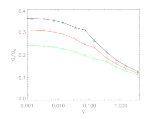
Fig. 1 depicts the time averaged conductance as a function of the source-drain bias for three different driving frequencies. In each case, the calculation starts from the zero bias limit reported previously NordlanderetAl00PRB . Driving with a lower frequency results in a larger conductance since the Kondo resonance can find more time to form during the time the dot level lies above its equilibrium position. As the bias is gradually increased, the conductance starts to decrease since the Kondo resonance starts to be quenched. However, Fig. 1 clearly shows that the conductance is enhanced considerably when the driving frequency is equal to the applied source-drain bias, deviating from the monotonous decreasing behaviour.
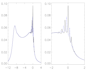
The origin of this phenomenon can be explained by noting that the finite bias induces a splitting of the Kondo resonance pinned to the Fermi level into two distinct Kondo peaks each located at the left and right reservoir’s Fermi levels and these split Kondo peaks are separated by the applied source-drain voltage. Furthermore, previous studies demonstrated that the ac driving generates sidebands of the split Kondo peaks due to the interference between the nonadiabatic photon-assisted processes and the Kondo tunneling. The separation of the satellite Kondo resonances from each split Kondo peak is an integer times the driving frequency . Therefore, when the driving frequency is equal to the source-drain bias, the first satellite resonance of each split Kondo peak overlaps with the other split Kondo peak. We believe this is the reason of the enhancement in the conductance. Fig. 2 displays all these features in the time averaged dot density of states, which is obtained by averaging the instantaneous dot density of states in a full period of oscillation. The instantaneous dot density of states is the Fourier transform of the retarded Green’s function and it is given by
| (4) |
The two broad peaks at =-1 and =-9 in the left panel correspond to the stationary states of the oscillation whereas the dip at =-5 is the equilibrium position of the dot. Right panel shows magnification of the left one around the Fermi level both at infinitesimal bias and when V=. All the features described above are visible here quite clearly.
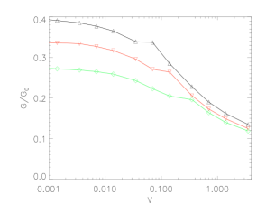
If the above hypothesis really holds, the enhancement would strongly depend on the ambient temperature. In order to verify the veracity of this argument, we calculated the conductance at the same frequencies in Fig. 1 for a lower temperature. The results are shown in Fig. 3. The enhancements at each frequency indeed increase compared to the higher temperature. Split Kondo peaks are more developed at lower temperature and so are their satellite resonances thus their overlap is more substantial giving rise to larger enhancement.
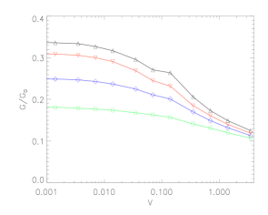
Finally, Fig. 4 shows the behaviour of the observed enhancement for a fixed oscillation frequency and various temperatures as a function of the source-drain bias. The enhancement is the largest at the lowest temperature since both the split and satellite Kondo peaks are fully developed. When we start decreasing the temperature the conductance at zero bias gets suppressed alongside with the enhancement at V= as the Kondo effect is gradually quenched. At the highest temperature the enhancement becomes indiscernible. The Kondo resonance even at zero bias is not developed sufficiently at this temperature hence the reduction of the conductance as a function of the bias is not as dramatic as lower temperatures. Therefore, the overlap of the sidebands with the split peaks creates negligible enhancement.
In conclusion, the non-crossing approximation was employed to investigate the effect of finite bias on time averaged conductance in single electron transistor when the dot level is driven sinusoidally by means of a gate voltage. Our results indicate that the time averaged conductance displays significant enhancement from its monotonous decrease when the driving frequency is equal to the applied source-drain bias. The enhancement tends to increase with decreasing temperature. We attributed this behaviour to the overlap of the split Kondo peaks pinned to each contact’s Fermi level with the satellite Kondo resonances. We expect this effect to be observable with present day experimental techniques which can directly probe current voltage characteristics. We thus hope to motivate new experiments in this field with this Brief Report.
A.G is extremely grateful to NSERC for providing generous financial support.
References
- (1) Ng T K and Lee P A 1988 Phys. Rev. Lett. 61 1768
- (2) Glazman L I and Raikh M E 1988 JETP Lett. 47 452
- (3) Goldhaber-Gordon D, Shtrikman H, Mahalu D, Abusch-Magder D, Meirav U and Kastner M A 1998 Nature 391 156–159
- (4) Goldhaber-Gordon D, Gores J, Kastner M A, Shtrikman H, Mahalu D and Meirav U 1998 Phys. Rev. Lett. 81 5225–5228
- (5) Cronenwett S M, Osterkamp T H and Kouwenhoven L P 1998 Science 281 540–544
- (6) Kondo J 1964 Prog. Theor. Phys. 32 37
- (7) Kouwenhoven L P and Glazman L 2001 Phys. World 14 33
- (8) Nordlander P, Pustilnik M, Meir Y, Wingreen N S and Langreth D C 1999 Phys. Rev. Lett. 83 808–811
- (9) Plihal M, Langreth D C and Nordlander P 2000 Phys. Rev. B 61 R13341–13344
- (10) Schiller A and Herschfield S 2000 Phys. Rev. B 62 R16271–R16274
- (11) Merino J and Marston J B 2004 Phys. Rev. B 69 115304
- (12) Plihal M, Langreth D C and Nordlander P 2005 Phys. Rev. B 71 165321
- (13) Anders F B and Schiller A 2005 Phys. Rev. Lett. 95 196801
- (14) Anders F B and Schiller A 2006 Phys. Rev. B 74 245113
- (15) Izmaylov A F, Goker A, Friedman B A and Nordlander P 2006 J. Phys.: Condens. Matter 18 8995–9006
- (16) Goker A, Friedman B A and Nordlander P 2007 J. Phys.: Condens. Matter 19 376206
- (17) Hettler M H and Schoeller H 1995 Phys. Rev. Lett. 74 4907
- (18) Schiller A and Hershfield S 1996 Phys. Rev. Lett. 77 1821
- (19) Goldin Y and Avishai Y 1998 Phys. Rev. Lett. 81 5394
- (20) Kaminsky A, Nazarov Y V and Glazman L I 1999 Phys. Rev. Lett. 83 384
- (21) Nordlander P, Wingreen N S, Meir Y and Langreth D C 2000 Phys. Rev. B 61 2146–2150
- (22) Kogan A, Amasha S and Kastner M A 2004 Science 304 1293
- (23) Scheible D V, Weiss C, Kotthaus J P and Blick R H 2004 Phys. Rev. Lett. 93 186801
- (24) Parks J J, Champagne A R, Hutchison G R, Flores-Torres S, Abruna H D and Ralph D C 2007 Phys. Rev. Lett. 99 026601
- (25) Al-Hassanieh K A, Busser C A, Martins G B and Dagotto E 2005 Phys. Rev. Lett. 95 256807
- (26) Kiselev M N, Kikoin K, Shekhter R I and Vinokur V M 2006 Phys. Rev. B 74 233403
- (27) Shao H X, Langreth D C and Nordlander P 1994 Phys. Rev. B 49 13929–13947
- (28) Jauho A P, Wingreen N S and Meir Y 1994 Phys. Rev. B 50 5528