Photovoltage Dynamics of the Hydroxylated Si(111) Surface Investigated by Ultrafast Electron Diffraction
Abstract
We present a novel method to measure transient photovoltage at nanointerfaces using ultrafast electron diffraction. In particular, we report our results on the photoinduced electronic excitations and their ensuing relaxations in a hydroxyl-terminated silicon surface, a standard substrate for fabricating molecular electronics interfaces. The transient surface voltage is determined by observing Coulomb refraction changes induced by the modified space-charge barrier within a selectively probed volume by femtosecond electron pulses. The results are in agreement with ultrafast photoemission studies of surface state charging, suggesting a charge relaxation mechanism closely coupled to the carrier dynamics near the surface that can be described by a drift-diffusion model. This study demonstrates a newly implemented ultrafast diffraction method for investigating interfacial processes, with both charge and structure resolution.
pacs:
82.53.Mj, 61.05.J-, 68.49.Jk, 82.65.+rThe problem of directly converting solar energy into electrical energy through photocarrier generation has recently gained tremendous attention due to new types of photovoltaic (PV) cells utilizing nanoparticles and molecular interfaces. Huynh et al. (1999); Gratzel (2001); Nozik (2002); Kelzenberg et al. (2007); Leschkies et al. (2007) An important parameter determining the efficiency of the solar cell is the survival rate of photogenerated carriers reaching the electrodes, which is strongly affected by surface recombination and the transport characteristics at the contacts. In a Schottky-type PV junction, the carrier dynamics are driven by a space-charge barrier layer. Schottky (1930) A photovoltage is generated as the photoinduced electron-hole pairs near the semiconductor interface move to reduce the band-bending. More generally, diffusion of non-equilibrium carriers, Davydov (1938); Mott (1939); Tauc (1957) charging of the surface states, Halas and Bokor (1989) and photoionization Demuth et al. (1986) are different contributors for emfs at semiconductor junctions, attributing to the overall magnitude and sign of the generated photovoltage. For a molecular interface, the existence of discrete surface and/or charge transfer states are crucial in directing the carrier separation in new generation PV cells, such as dye-sensitized TiO2 mesoporous films Gratzel (2001) and quantum dot solar cells. Nozik (2002); Leschkies et al. (2007) In these cases, the filling of a surface state can strongly affect the charge distribution in the space-charge layer, modifying the transport characteristics, as revealed in photoemission studies. Halas and Bokor (1989); Long et al. (1990); Marsi et al. (2000) Surface charging is also essential for explaining surface photochemical processes, including catalysis Yoon et al. (2005) and molecular transport. Liang et al. (2004) Here, we use a novel diffractive potentiometry approach to determine the transient photovoltage based on the ultrafast electron diffraction (UED) technique, whose ability to resolve surface structure evolution has been demonstrated previously. Zewail (2006); Ruan et al. (2007)
We study the photoinduced surface potential changes on a Si(111) surface terminated with hydrophilic hydroxyl (OH) groups, a prototypical system for fabricating molecular electronic devices. Shipway et al. (2000); Aswal et al. (2006) The experiment is performed in an optical pump
 diffraction probe arrangement, in which the femtosecond laser pulse is used to initiate carrier
generation near the surface and in turn, the formation of a transient surface voltage (TSV), while a charge
sensitive electron pulse probes the ensuing carrier relaxation dynamics. A Coulomb refraction formalism is deduced to treat ultrafast diffraction data to determine the TSV. Using a laser fluence () of 22 mJ/cm2, we found a band-flattening TSV of 300 mV generated 30 ps after the laser excitation. At higher fluences ( mJ/cm2), the TSV continued to rise, even beyond the bandgap energy. This surprisingly large TSV is attributed to a modified barrier due to a non-equilibrium surface charge migration, induced by photoexcitation. Marsi et al. (2000) We observed picosecond charge injection and relaxation dynamics with timescales similar to results obtained using ultrafast photoemission studies of surface carrier dynamics in a vacuum cleaved Si(111)-() surface. Halas and Bokor (1989) This rapid recovery can be understood based on a drift-diffusion model that couples surface carrier dynamics with transport in the space-charge layer. This suggests that the hydroxylated silicon surface posseses a lower concentration of trap states, ideal for mediating molecular electronic transport study. Aswal et al. (2006)
The hydroxylated Si(111) surface was prepared ex situ using a wet chemistry method. The as received Si(111) wafer (Silicon Quest Intl., p-type, roughness m) was treated with a modified RCA procedure. Kern and Puotinen (1970) The native oxide layer, which usually contains a high density of trap states, was removed and an ultrathin ( 5 nm) thermal oxidation layer with high electric quality was grown. First, the wafer was immersed in H2SO4/H2O2 (7:3) solution at for 10 min to remove surface contaminants. The surface was then etched with a saturated NH4F solution Higashi et al. (1991) to remove the native oxide layer, followed by a bath in NH4OH/H2O2/H2O (1:1:5) at for 20 min to further remove inorganic residues. Finally, a thin layer of oxide that affords a hydroxylated surface was grown by immersing the wafer in HCl/H2O2/H2O (1:1:6) at for 10 min. The wafer was rinsed with deionized water ( Mcm) for 10 min at the end of each cycle. This procedure yields a density of cm-2 silanol groups (Si-OH) on the surface. Aswal et al. (2006)
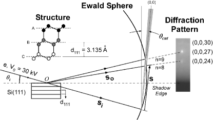
The experiment was conducted in the ultrafast electron crystallography setup, Ruan et al. (2007) employing the reflection geometry to gain surface sensitivity. As described in Fig. 1, the incident probe electron has a kinetic energy = , where = 30 kV is the accelerating voltage, corresponding to an incident reciprocal wavevector = 90 Å-1. At an incidence angle, = , the Ewald sphere intersects the (0,0) reciprocal lattice rod of the Si(111) substrate near momentum transfer wavevector Å-1, producing an in-phase (0,0,27) diffraction maximum on the screen. Since the Si(111) substrate has a slight miscut, ( ), the diffraction maxima appear slightly below the projected Zeroth Order Laue Zone. Weak (0,0,24) and (0,0,30)PEA diffraction maxima arising from the surface roughness were also observed. These maxima are associated with the interference pattern of Si(111) planes, evident from = 1.985 Å-1 between neighboring peaks satisfying the reciprocal relationship = 2 with an accepted value of 3.135 Å. The electron penetration depth in silicon is estimated to be 2 nm based on the Scherrer criterion, Patterson (1939) using the width of the (0,0,27) diffraction maximum.
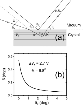
To determine the surface potential, we examine the Coulomb refraction introduced by a surface potential for electron diffraction, as shown in Fig. 2(a). The surface potential, , alters the kinetic energy of the electrons submerged in the crystal, = , without changing the transverse momentum, thereby causing a refraction at the interface. The index of refraction can be described by . Wang (1996) For surface diffraction, this alters the electron incidence angle towards the lattice plane, thus introducing a net angular shift () of the diffraction maximum. We calculate the shift arising from a surface potential to be
| (1) |
where all symbols are defined in Fig. 2(a). In the optical pump diffraction probe experiment, $V_s$ is replaced by the transient surface voltage, $\Delta V_s$, to evaluate the photoinduced refraction shift of diffraction maxima at $\theta_o$. The dependence of $\delta$ on $\theta_o$ is shown in Fig.~\ref{Fig2}(b), calculated using Eqn.(\ref{Eqn1}) with our incidence angle ($\theta_i$ = $6.8\,^{\circ}{\rm}$) and $\Delta V_s = 2.7$ volts. This refraction shift has a ‘nonstructural’ characteristic, exhibiting a more significant deviation at smaller values of . This differs fundamentally from structure-induced shifts, which behave oppositely. For small angle diffraction the Bragg law yields a monotonic increase in as a function of for a given structural change , described by , i.e. the higher order diffraction maxima experience proportionally larger shifts than the lower order ones. This clear distinction allows us to separate Coulomb-induced effects from structural changes by analyzing multiple diffraction maxima.
To demonstrate the principle, we will follow both (0,0,24) and (0,0,27) diffraction maxima to examine the TSV dynamics.
The characteristic features associated with the Coulomb effect were observed experimentally as shown in Fig. 3(a). Using a laser fluence of 72 mJ/cm2, the time-dependent shifts of diffraction maxima (0,0,24) and (0,0,27) were followed by adjusting the arrival time of the electron probe pulse relative to that of the exciting laser pulse. The shift of the (0,0,24) diffraction maximum in reciprocal space is markedly greater than that associated with (0,0,27), pointing to a Coulomb effect. We expect a negligible structure-induced shift because of the small absorption coefficient in silicon (m) for the near infrared excitation (1.55 eV), indicating that the thermal energy deposition is spread out over a large volume. The maximum temperature rise in Si can be estimated from , where is the reflectivity, Jm-3K-1 is the lattice heat capacity, and is the carrier density drop due to Auger recombination. Chen et al. (2005) The laser fluences we applied ranged from 22 to 72 mJ/cm2, which give rise to only moderate increases in lattice temperature, about 20 to 170 K, respectively, above the initial temperature, = 300 K. Hence the changes induced by lattice heating, , are on the order of based on the thermal expansion coefficient for Si. Glazov and Pashinkin (2001) In contrast, the carrier generation is more significant, ranging from to cm-3, which corresponds to an increase of several orders of magnitude from the intrinsic carrier concentration ( cm-3) within the first ps. Chen et al. (2005) It is expected that such a large increase in carrier density will easily flatten out the initial surface band-bending, which is V, Widdra et al. (2003) leading to a change for the (0,0,27) maximum. Indeed, a band-flattening TSV of 0.38 V was determined at the lowest fluence applied ( = 22 mJ/cm2). However, TSVs higher than the initial band-bending were also observed; 1.74 and 2.97 V for fluences of 46 and 72 mJ/cm2, respectively. In Fig. 3(b), the TSVs deduced from Eqn.(1) are consistent for both the (0,0,24) and (0,0,27) maxima, for all three fluences, demonstrating the robustness of the diffractive TSV measurment.
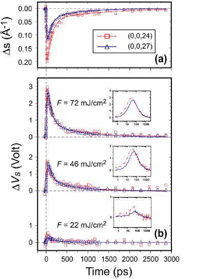
The significant photovoltage induced by the high fluence femtosecond laser cannot be explained merely by a barrier-layer effect, where photoinduced e-h pairs near the semiconductor interface separate to screen the surface charges responsible for the band-bending. Without modifying surface charge population, this theory would predict a maximum TSV corresponding to the dark current band-bending Kronik and Shapira (1999) and the decay time of the TSV would be comparable to the characteristic bulk recombination time ( ns for Si). This is not what is observed here. In contrast, we have witnessed a much more rapid process, with the TSV surging within 30 ps following laser excitation and a decay on the order of 100 ps for each of the three different fluences, without any saturation, as shown in Fig. 3(b). Enhanced surface band-bending was also observed by Marsi et al. in studying the transient charge distribution at the SiO2/Si interface following UV free electron laser excitation using time-resolved pump-probe core photoemission spectroscopy. Marsi et al. (2000) The cause of the enhancement is attributed to electron diffusion into the thermally grown SiO2 overlayer and subsequent accumulation at its surface. The recombination of the excess electrons was found to be slower with thicker oxide layers. For 12 Å oxide thickness, the surface charge recombination was found to be comparable to the typical excess carrier recombination time in the Si(111) space-charge layer, of the order of 100 ns. For very thin (a few Å) oxide layers, a very effective ‘surface’ recombination process was observed within their time resolution of 200 ps. These observations are consistent with a picture in which the surface recombination rate is determined by the separation between the excess surface electrons and excess holes in the Si space-charge layer. Indeed, much shorter recombination time is found for the decay of the surface state population in a vacuum-cleaved Si surface. Halas and Bokor (1989) This speed-up in surface recombination for an ultrathin oxide layer ( nm) observed by Marsi et al. is attributed to the enhanced overlap of bulk evanescent states of Si with the surface states. In that case and in the studies reported here, the electrons accumulated at the thin oxide surface are so close to the Si space-charge layer that their role in the recombination process is similar to the normal surface state.
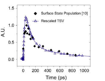
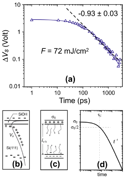
The decay behavior of the TSV on the hydoxylated Si(111) surface was compared with the surface state dynamics on a vacuum-cleaved Si(111)-() surface, revealed by a photoemission study (Fig. 4). Halas and Bokor (1989) In this figure, the TSV is rescaled to match with the data extracted from Ref. 10. We find a striking similarity between the two, suggesting that the surface state population is in quasi-equilibrium with the bulk carrier dynamics in the space-charge layer, so long as there is strong coupling between the surface state and the bulk evanescent state. Further evidence of the strong role played by carrier dynamics on the surface recombination is revealed by the power-law decay of the TSV, shown in Fig. 5(a), where an exponent near -1 (-0.930.03) is ascribed to the characteristic decay of surface charges, with a time constant of 100 ps.
To describe the population decay of the surface state driven by a space-charge drift recombination, we introduce a simple two-slab model, illustrated in Fig. 5(b)-(d). The electrons accumulated at the surface lead to a rapid rise in surface potential within the thin oxide layer that decays slowly into the Si space-charge region, as depicted in Fig. 5(b). The non-equilibrium space-charge layers, with initial separated charge density , are modeled as two separate slabs, separated by a distance in a dielectric medium ( for Si), shown in Fig. 5(c). The power-law characteristics are manifested in the simple rate equation , with the space-charge recombination time depending on the transient field , which is directly related to the surface charge . Its solution has a characteristic timescale , which is the time for the TSV to drop by 50% from its initial value, and corresponds to the induction period in the log-log plot of the solution, as described in Fig. 5(d). For , the behavior emerges, similar to what is observed experimentally [Fig. 5(a)]. To compare with the experimental results, we assume a linear decay of the surface potential barrier () over the space-charge layer , and determine the size of the induced space-charge regime to be nm (using carrier mobility, =100 cm2V according to Ref. 25, our measured of 100 ps, and of 2 V), which is in agreement with the laser penetration depth in Si.
Other mechanisms that would also affect the TSV decay include the ambipolar diffusion of the bulk excess carriers away from the surface and the decay of the surface state charges into trap states. Here, we can exclude ambipolar diffusion as the main cause for TSV decay for two reasons. First, the characteristic diffusion time, , is significantly longer than what we observed ( ps, based on the excess e-h region generated by the laser, 1 m, and ambipolar diffusivity 15 cm2s-1). Chen et al. (2005) Second, a decay is expected in the case of one-dimensional diffusion, Yang et al. (2007) which is appropriate for photoexcitation when the laser spot size (600 m) is large compared to the penetration depth (m). The rapid decay of the TSV after 100 ps precludes any long-lived trap state from playing a significant role. Halas and Bokor invoked coupled drift-diffusion-Poisson equations for bulk carriers to self-consistently treat the surface state dynamics. Halas and Bokor (1989) Such a calculation is able to describe the general behavior of the surface state depopulation and TSV decay (to be reported elsewhere Murdick et al. ). However, the essential power-law behavior can be elucidated with a simple space-charge recombination model, as described above.
While the simple Coulomb refraction formalism described in Eqn.(1) seems to be adequate for deducing consistent TSVs from diffraction maxima, especially for the recombination dynamics, some departure between the TSVs deduced for (0,0,24) and (0,0,27) is evident at short times, as depicted in the insets of Fig. 3(b). This discrepancy is believed to be caused by a non-equilibrium barrier layer, which deviates significantly from a homogeneous potential model assumed in Eqn.(1) within the electron probed volume. More rigorous treatment of the Coulomb refraction formalism with a non-homogeneous potential is needed to fully account for the short-time dynamics.
In conclusion, we have demonstrated a new method of directly measuring transient surface potential using ultrafast electron diffraction. In comparison with other commonly used surface imaging techniques, such as Kelvin Force and Scanning Tunneling Microscopy, we are able to examine surface potential changes from the femtosecond to nanosecond timescale. This technique is complementary to ultrafast photoemission methods in which the energetics of the photoemitted electrons, rather than the potential, are directly measured. Since our employed electron probe energy is reasonably high, it allows surface potential characterization at high laser excitation fluences, which are usually inaccessible by the low energy photoemission techniques due to the space-charge effect. Gilton et al. (1990) We have revealed a regime of strong photoinduced surface voltage rise, which can serve as an impulsive current source for investigating time-dependent transport at nanointerfaces.
This work was supported by Department of Energy under grant DE-FG02-06ER46309.
References
- Huynh et al. (1999) W. U. Huynh, X. G. Peng, and A. P. Alivisatos, Adv. Mat. 11, 923 (1999).
- Gratzel (2001) M. Gratzel, Nature 414, 338 (2001).
- Nozik (2002) A. J. Nozik, Physica E 14, 115 (2002).
- Kelzenberg et al. (2007) M. D. Kelzenberg, D. B. Turner-Evans, B. M. Kayes, M. A. Filler, M. C. Putnam, N. S. Lewis, and H. A. Atwater, Nano Lett. 8, 710 (2007).
- Leschkies et al. (2007) K. S. Leschkies, R. Divakar, J. Basu, E. Enache-Pommer, B. J. E., C. B. Carter, U. R. Kortshagen, D. J. Norris, and E. S. Aydil, Nano Lett. 7, 1793 (2007).
- Schottky (1930) W. Schottky, Physik Z. 31, 913 (1930).
- Davydov (1938) V. I. Davydov, Tech. Phys. USSR 5, 79 (1938).
- Mott (1939) N. F. Mott, Proc. Roy. Soc. London A 171, 281 (1939).
- Tauc (1957) J. Tauc, Rev. Mod. Phys. 29, 308 (1957).
- Halas and Bokor (1989) N. J. Halas and J. Bokor, Phys. Rev. Lett. 62, 1679 (1989).
- Demuth et al. (1986) J. E. Demuth, W. J. Thompson, N. J. DiNardo, and R. Imbihl, Phys. Rev. Lett. 56, 1408 (1986).
- Long et al. (1990) J. P. Long, H. R. Sadeghi, J. C. Rife, and M. N. Kabler, Phys. Rev Lett. 64, 1158 (1990).
- Marsi et al. (2000) M. Marsi, R. Belkhou, C. Grupp, G. Panaccione, A. Taleb-Ibrahimi, L. Nahon, D. Garzella, D. Nutarelli, E. Renault, R. Roux, et al., Phys. Rev. B 61, R5070 (2000).
- Yoon et al. (2005) B. Yoon, H. Hakkinen, U. Landman, A. S. Worz, J. M. Antonietti, S. Abbet, K. Judai, and U. Heiz, Science 307, 403 (2005).
- Liang et al. (2004) G. C. Liang, A. W. Ghosh, M. Paulsson, and S. Datta, Phys. Rev. B 69, 115302 (2004).
- Zewail (2006) A. H. Zewail, Ann. Rev. Phys. Chem. 57, 65 (2006).
- Ruan et al. (2007) C.-Y. Ruan, Y. Murooka, R. K. Raman, and R. A. Murdick, Nano. Lett. 7, 1290 (2007).
- Shipway et al. (2000) A. N. Shipway, E. Katz, and I. Willner, Chem. Phys. Chem. 1, 18 (2000).
- Aswal et al. (2006) D. K. Aswal, S. Lenfant, J. V. Guerin, D. Yakhmi, and D. Vuillaume, Ana. Chim. Acta 568, 84 (2006).
- Kern and Puotinen (1970) W. Kern and D. A. Puotinen, RCA Rev. 31, 187 (1970).
- Higashi et al. (1991) G. S. Higashi, R. S. Becker, Y. J. Chabal, and A. J. Becker, Appl. Phys. Lett. 58, 1656 (1991).
- (22) The signal-to-noise ratio for this peak was too weak to follow dynamically.
- Patterson (1939) A. L. Patterson, Phys. Rev. 56, 978 (1939).
- Wang (1996) Z. L. Wang, Reflection Electron Microscopy and Spectroscopy for Surface Analysis (Cambridge University Press, New York, 1996).
- Chen et al. (2005) J. K. Chen, D. Y. Tzou, and J. E. Beraun, Int. J. Heat and Mass Trans. 48, 501 (2005).
- Glazov and Pashinkin (2001) V. M. Glazov and A. S. Pashinkin, High. Temp. 39, 413 (2001).
- Widdra et al. (2003) W. Widdra, D. Brocker, T. Giessel, I. V. Hertel, W. Kruger, A. Liero, F. Noack, V. Petrov, D. Pop, P. M. Schmidt, et al., Surf. Sci. 543, 87 (2003).
- Kronik and Shapira (1999) L. Kronik and Y. Shapira, Surf. Sci. Rep. 37, 1 (1999).
- Yang et al. (2007) D.-S. Yang, N. Gedik, and A. H. Zewail, J. Phys. Chem. C 111, 4889 (2007).
- (30) R. A. Murdick, C.-Y. Ruan, and R. E. Mickens, in preparation. Electron and hole motions are described by the Drift-Diffusion-Poisson (DDP) coupled PDEs. We integrate the field from the DDP system over our probe depth, allowing us to compare the numerically calculated with our measured values. Numerical integration of the DDP system is carried out via non-standard finite difference (NSFD) scheme, which enforces positivity on electron-hole densities.
- Gilton et al. (1990) T. L. Gilton, J. P. Cowin, G. D. Kubiak, and A. V. Hamza, J. Appl. Phys. 68, 4802 (1990).