Defect-free ZnSe nanowire and nano-needle nanostructures
Abstract
We report on the growth of ZnSe nanowires and nano-needles using molecular beam epitaxy (MBE). Different growth regimes were found, depending on growth temperature and the Zn–Se flux ratio. By employing a combined MBE growth of nanowires and nano-needles without any post-processing of the sample, we achieved an efficient suppression of stacking fault defects. This is confirmed by transmission electron microscopy and by photoluminescence studies.
Semiconductor nanowires (NWs) have attracted much attention in recent years because of their properties and potential use in a variety of technological applications. NW heterostructures are interesting candidates for the development of well-located and size-controlled quantum dots (QDs) NW-QD . Due to the narrow lateral size, QD heterostructures in NWs can be directly grown on very defined positions and without the necessity of self-assembly. This is an especially interesting feature for II-VI materials, where self-assembled island formation occurs only within narrow windows of growth conditions RobinAPL . Recently, II-VI compound semiconductor NWs have been synthesized by Au-catalysed metal-organic chemical vapour deposition (MOCVD) and molecular-beam epitaxy (MBE) methods NW-MOCVD ; NW-MBE . An obstacle towards the growth of optically active NW heterostructures are donor–acceptor pairs that form in defects Philipose2 . These cause a strong spectral background which competes with the excitonic emission in the QDs. Ref. Philipose1 reports the efficient reduction of this spectral background after annealing of the NW samples in Zn-rich atmosphere.
When developing NW heterostructures, annealing or other post-growth processing of the sample is often unfavourable as it may also influence the designed form of the heterostructure through inter-diffusion of the constituents. Instead, growth methods, that directly avoid the formation of defects are desired. In this letter, we report a growth recipe for ZnSe NWs, where the amount of stacking fault defects is strongly reduced. This was achieved by a combined growth of NWs and nano-needles without any post-growth processing of the sample.
The ZnSe NWs were grown in the vapour-liquid-solid growth mode with gold particles as catalysts. For comparison, GaAs(001) and Si(001) substrates were used. Degased surfaces for MBE growth were obtained after annealing in ultra-high vacuum at 580∘ C. In the case of GaAs, the effect of an epitaxial GaAs buffer layer was also investigated. Interestingly the structural properties of the NWs depend very little on the utilized substrate. Next, a thin gold film with thickness of 0.2–0.5 nm was deposited on the GaAs substrates inside an electron beam metal deposition chamber. The gold film was dewetted to a droplet-like surface by annealing the sample at C for 5 min. ZnSe MBE growth was then performed with varying growth conditions. The sample transfers between the MBE- and metal deposition chambers happened under ultra-high vacuum.
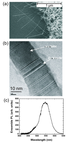
When growing under an excess of Se (Zn (Se) flux: 2.5 (7.5) torr) and a sample temperature of 350–450∘ C, a dense carpet of narrow NWs with high aspect ratios covers the substrate. The NWs have a uniform diameter of 20–50 nm and a length up to 2 m after a growth of one hour (fig. 1(a)). Additionally to the NWs, the as-grown substrate is covered with highly irregular nano-structures. Fig. 1(b) shows a transmission electron microscopy (TEM) image of one NW. The crystal structure of the NWs are predominantly wurtzite. However, the NWs are systematically intersected with regions of zinc blende phase. We account for the formation of such defects and the presence of highly irregular structures by non-ideal growth conditions at the initial stages of the growth process. Possible reasons are the presence of non-uniform gold agglomerations instead of small gold beads and the insertion of impurities during the gold deposition process. The presence of both wurtzite and Zn-blende shows, that at the utilized growth conditions both phases are allowed. Although, the observation of wurtzite structure is in contrast to the Zn-blende that naturally occurs in bulk ZnSe, it is not an uncommon behaviour for NWs, as discussed in ref. Glas_Wurtzite .
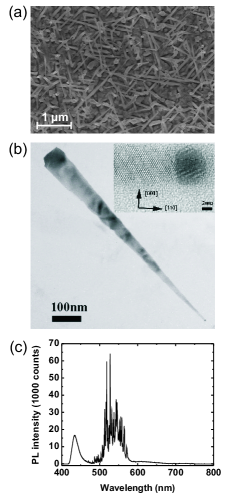
When, on the other hand, growing at low temperature (300∘ C) or with inverted Zn:Se flux ratio, needle-shaped NWs are formed (fig. 2(a)). Hereafter we will refer to those nanostructures as nano-needles to distinguish them from the narrow NWs described previously. By TEM (fig. 2(b)) we determined that the nano-needles have a wide base (80 nm in diameter) and a sharp tip (5- 10 nm). We also observed darker and lighter regions which again indicate the presence of stacking fault defects. The formation of nano-needles instead of NWs is well accounted for by the slower adatoms mobility expected at low temperature or at low Se flux. The slower mobility promotes nucleation on the sidewalls before reaching the gold catalyst at the nano-needle tip. Moreover, we observed that the nano-needles are predominantly wurtzite, as for NWs, but the wire axis is here perpendicular to the c-axis instead of being parallel. In contrast also to the long NWs (in fig. 1), the defect planes are here disoriented with respect to the nano-needle axis. It seems that this disorientation hinders the propagation of defects in the growth direction, especially for lower diameters. Defects zones are rapidly blocked on the side walls, providing a high structural quality towards the nano-needle tip.
To carry out single-NW studies, the sample is put in a methanol ultra-sonic bath for 30 s in order to detach some NWs from the substrate. Droplets of this solution are next placed on a fresh substrate, leaving behind a low density of individual NWs. Ensemble spectra were taken on the as-grown sample. All spectra in this paper were measured at a sample temperature of 5 K. The photoluminescence (PL) of individual NWs were excited with a cw laser at 405 nm via a microscope objective.
Both for NWs and nano-needles, we observe a broad spectral distribution within 500–600 nm, as seen in figs. 4(a) and (b). Even in the case of a single nano-needle, the spectrum is dominated by many intense spectral lines, which we attribute to emission from excitons localized at the defect zones in the NW Philipose2 . In contrast to the observations in ref. Philipose1 on MOCVD-grown NWs, we do not see an enhancement of the ZnSe band edge emission (443 nm at 5 K Malikova ) when growing under Zn-rich conditions. The intense emission with 500–600 nm instead suggests that in both cases (NWs and nano-needles), point defects effectively capture the excited charge carriers and quench the band edge emission, as also reported in Ref. Xiang_noBE . This is in agreement with the high density of stacking fault defects observed by TEM.
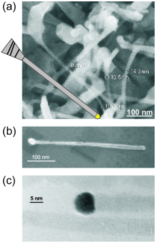
The observation of a decreasing defect density from the base towards the top in the nano-needles motivated us to modify the growth recipe in the following way: In the first partf, the sample is grown with excess of Zn for 30 min, leading to the formation of nano-needle structures. Next, the Zn- and Se-flux was inverted and NWs were grown for another 30 min on top of the nano-needles. Thus, the growth at the side-walls was aborted and re-growth started on defect-free and strain-relaxed nano-needle tips, where the high structural quality of the crystal lattice can be preserved along the narrow NW that is now formed in this second growth step. Fig. 3 shows results obtained from this sample. The structures have a broad base that tapers after a few ten nanometers to thin NWs with thickness of 10–15 nm. As symbolized in the sketch in fig. 3(a) we expect that stacking faults reduce towards the thin part of the NW, which is indeed the case, as seen in TEM images of a single NW, fig. 3(c).
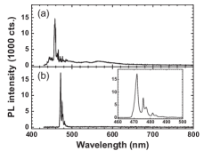
The suppression of defects has a strong effect on the PL of these nano-structures (fig 4). Due to the low density of defects, the spectral emission between 500-600 nm that was observed before from the samples in figs 4(a) and (b) is strongly reduced, leaving behind only a small bunch of intense spectral lines between 450–500 nm. The weak and broad distribution between 500–600 that remains in the ensemble PL, fig 4(c), is due to excitons localized in defects in the thicker NW base. In the spectrum of a single NW that broke off behind the thicker base, fig 4(d), this broad background is now globally suppressed. In spite of this, no PL is observed at the ZnSe band-edge. A possible reason is that, due to the very thin diameter of the NWs, additional surface states may form in the bandgap Schmidt_Surface_InP_NWs and introduce non-radiative decay channels that quench the band-edge PL. The remaining narrow PL peaks around 470 nm in fig. 4(d) can very likely be assigned to residual impurities responsible for donor-acceptor pair emission and their related phonon replica Polimeni_ZnSeO .
In summary we have reported on MBE growth of ZnSe NWs. Depending on growth temperature and Zn-Se flux ratio, we can tailor the structures between thin NWs with homogeneous thickness of 20–50 nm, and nano-needles with broad base and a sharp tip with 5–10 nm thickness. By combining nano-needle and NW growth, we achieved the growth of mostly defect-free structures, without any post-growth treatment of the sample. This is confirmed by TEM and PL measurements. In the latter, the emission of excitons localized in the defect zones was strongly reduced. The suppression of defects is an important pre-condition for developing QD heterostructures inside NWs. In a next step, we included CdSe zones into the NW in order to form QDs. This will be reported in a subsequent publication.
Acknowledgments
We are grateful to V. Zwiller for inspiring discussions. T.A. acknowledges support by Deutscher Akademischer Austauschdienst (DAAD).
References
- (1) M. T. Borgström, V. Zwiller, E. Müller, and A. Imamoglu, Nanoletters 5, 1439 (2005).
- (2) I.-C. Robin, R. André, C. Bougerol, T. Aichele, and S. Tatarenko, Appl. Phys. Lett. 88, 233103 (2006).
- (3) R. Solanki, J. Huo, J. L. Freeouf, and B. Miner, Appl. Phys. Lett. 81, 3864 (2002).
- (4) Y. F. Chan, X. F. Duan, S. K. Chan, I. K. Sou, X. X. Zhang, and N. Wang, Appl. Phys. Lett. 83, 2665 (2003); A. Colli, S. Hofmann, A. C. Ferrari, C. Ducati, F. Martelli, S. Rubini, S. Cabrini, A. Franciosi, and J. Robertson, Appl. Phys. Lett. 86, 153103 (2005).
- (5) U. Philipose, S. Yang, T. Xu, and H. E. Ruda, Appl. Phys. Lett. 90, 063103 (2007).
- (6) U. Philipose, T. Xu, S. Yang, P. Sun, H. E. Ruda, Y. Q. Wang, and K. L. Kavanagh, J. Appl. Phys. 100, 084316 (2006).
- (7) F. Glas, J.-Ch. Harmand, and G. Patriarche, Phys. Rev. Lett. 99, 146101 (2007).
- (8) L. Malikova, W. Krystek, F. H. Pollak, N. Dai, A. Cavus, and M. C. Tamargo, Phys. Rev. B 54, 1819 (1996).
- (9) B. Xiang, H. Z. Zhang, G. H. Li, F. H. Yang, F. H. Su, R. M. Wang, J. Xu, G. W. Lu, X. C. Sun, Q. Zhao, and D. P. Yu, Appl. Phys. Lett. 82, 3330 (2003).
- (10) T. M. Schmidt, Appl. Phys. Lett. 89, 123117 (2006).
- (11) A. Polimeni, M. Capizzi, Y. Nabetani, Y. Ito, T. Okuno, T. Kato, T. Matsumoto, and T. Hirai, Appl. Phys. Lett. 84, 3304 (2004); B. A. Weinstein, T. M. Ritter, D. Strachan, M. Li, H. Luo, M. Tamargo, and R. Park, phys. stat. sol. (b) 198, 167 (1996).