A microwave transmission-line network guiding electromagnetic fields through a dense array of metallic objects
Abstract
We present measurements of a transmission-line network, designed for cloaking applications in the microwave region. The network is used for channelling microwave energy through an electrically dense array of metal objects, which is basically impenetrable to the impinging electromagnetic radiation. With the designed transmission-line network the waves emitted by a source placed in an air-filled waveguide, are coupled into the network and guided through the array of metallic objects. Our goal is to illustrate the simple manufacturing, assembly, and the general feasibility of these types of cloaking devices.
Keywords: Transmission-line network; scattering cross section; electromagnetic cloak.
I Introduction
The interest in different types of devices and materials for dramatic reduction of the total scattering cross sections of arbitrary or specific objects, has gained a large amount of interest after the publication of recent papers Leonhardt ; Pendry ; Alu ; Schurig . Earlier, the subject of hiding objects or particles from the surrounding electromagnetic fields was studied over the recent decades by many others as well, e.g., Kerker ; Chew ; Sihvola ; Kildal ; Greenleaf .
Recently, we have proposed an alternative approach to cloaking of objects composed of electrically dense arrays of small inclusions (in principle, these inclusions can be composed of arbitrary materials) Alitalo_cloak_TAP ; Alitalo_cloak_iWAT08 . Since these objects can be two-dimensional or even three-dimensional interconnected meshes of e.g. metallic rods, practical applications of these types of cloaks include hiding strongly scattering objects such as support structures situated close to antennas, creating filters (a “wall” or a slab letting through only a part of the spectrum of the incoming field), etc. Also, as it has been recently proposed, these networks offer a simple way of creating new types of matched lenses especially for microwave applications Alitalo_TLlens .
The goal of this paper is to experimentally demonstrate the simple manufacturing and assembly of the previously proposed transmission-line structure, where the transmission lines composing the network are realized as parallel metal strips. By measurements we confirm the previously predicted matching of the network with free space, as well as a possibility of transmission of fields through an electrically dense mesh of metal objects. These results demonstrate the benefits of this simple approach to cloaking and present an easy way to measure the performance of these types of periodic structures.
II Transmission-line network
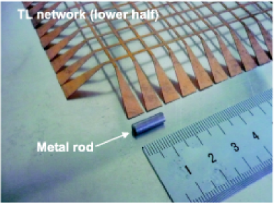
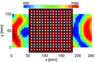
The transmission-line network that is used here is the same as designed in Ref. Alitalo_cloak_TAP , with the optimal impedance matching with free space observed around the frequency of 5.5 GHz. For this design, the matching with free space and the cloaking phenomenon were verified with full-wave simulations Alitalo_cloak_TAP . In this paper we demonstrate the simple manufacturing and assembly of this type of structure by choosing to use a two-dimensional periodic transmission-line network with a square shape and 16 16 unit cells in the network. The edges of the network are connected to a “transition layer” (parallel metal strips gradually enlarging from the ends of the network), as proposed in Ref. Alitalo_cloak_TAP .
By inserting the designed network inside a metallic parallel-plate waveguide (with the plates lying in the -plane), we effectively realize the same situation as would occur with an infinitely periodic array of networks with the periodicity along the -axis, since here the electric field is assumed to be parallel to the -axis (as in the example case that was studied previously Alitalo_cloak_TAP ). See Fig. 1 for an illustration of the transmission-line network with all the necessary dimensions of the structure included.
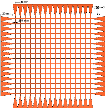
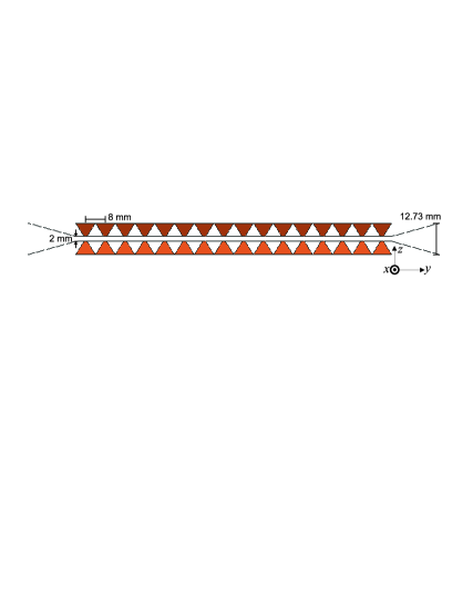
The structure shown in Fig. 1 was manufactured by etching from a thin copper plate. The network can be simply assembled from two similar profiles (each profile as shown in Fig. 1a) just by placing them on top of each other, as shown in Fig. 1b. Ideally, the volume between these two metal objects should be free space Alitalo_cloak_TAP . Here, due to practical reasons, we have placed small pieces of styrofoam (with material properties very close to those of free space) between the metal strips. For assembly purposes, pieces of styrofoam are placed also on top and below the metal strips for support. These styrofoam pieces naturally do not affect the propagation properties of the transmission lines since the fields are mostly confined between the parallel strips.
In Ref. Alitalo_cloak_TAP the reference object, i.e., the object that we wanted to cloak (hide) from the surrounding electromagnetic fields, was an array of infinitely long perfectly conducting rods (that fit inside the neighboring transmission lines of the network). Here, we use a similar periodic structure as a reference object through which we want to guide the fields. The individual inclusions of this reference object are metal cylinders (parallel to the -axis) with the same height as the network (13 mm). The diameter of these cylinders is 4 mm and there are a total of 15 15 cylinders in the array.
III Measurement setup
The measurement setup that is used here is similar to the one presented in Ref. Schurig . With our measurements we effectively simulate an infinitely periodic structure with the periodicity in the vertical (-) direction, by introducing a measurement cell consisting of a parallel-plate waveguide with its metallic plates lying in the -plane. Because of the image principle (the electric fields are assumed to be mostly parallel to the -axis inside the waveguide), we can thus measure only one period of the structure. The difference between the measurement setup used here and the one in Ref. Schurig is that here the upper plate of the waveguide is formed by a dense wire mesh, that lets through a fraction of the field inside the waveguide, instead of having a solid metallic upper plate with a hole for the probe, as was used in Ref. Schurig . The mesh that we use here is the same as the one used in Ref. Maslovski , i.e., the mesh is a thin copper plate, in which square holes of size 4 mm 4 mm have been etched with the period of the holes being 5 mm. A small part of the field gets through this mesh and we can measure that field with a probe placed on top of the waveguide Maslovski .
To simplify the measurement, we excite a cylindrical wave inside the waveguide with a feed probe (a coaxial probe placed inside the waveguide) and measure the transmission from this probe to the other probe (“measurement probe”, placed on top of the waveguide) with a vector network analyzer (VNA, Agilent E8363A). The use of the metal mesh as a part of the top plate of the waveguide (rather than using a probe inside the waveguide) ensures that the measurement probe does not disturb the field inside the waveguide. The measurement probe on top of the waveguide is stationary, and the waveguide is moved with a PC-controlled scanner, synchronized with the VNA for precise measurements in the wanted coordinate positions. These points where the measurement of the complex -parameter are taken with the VNA, can be arbitrarily chosen with the PC-program running the scanner. All the measurements presented in this paper were done with the steps of 5 mm. As the measured area is 240 mm 100 mm, we will have the complex measured at 49 different points in the -plane.
The probe that we use here is a monopole oriented along the -axis and positioned approximately at 3 mm away from the metal mesh. The probe is intentionally poorly matched at the frequencies of interest (5 GHz – 6 GHz) in order to make sure that the measurement probe does not disturb the fields inside the waveguide. The high dynamic range of the VNA makes sure that we can measure the electric field distribution inside the waveguide even with this poorly matched probe.
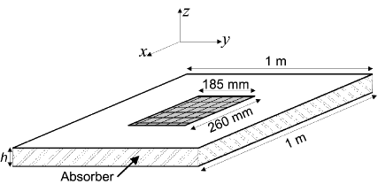
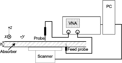
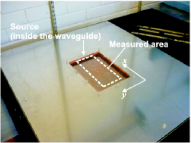
See Fig. 2 for an illustration of the measurement setup. The parallel-plate waveguide that we use here has the width and length of 1 m, and the height mm (ideally should be equal to 12.73 mm Alitalo_cloak_TAP ). A part of the upper plate is removed from the center for the placing of the metal mesh (the area above which we want to measure the field distributions). The area of this mesh is 260 mm 185 mm. The measurable area is further restricted by the used scanners. We have used two scanners, one with the movement limited to 300 mm (-axis) and one with the movement limited to 100 mm (-axis). The area to be measured has been decided to be 240 mm 100 mm, centered in the mesh area. The feed probe is positioned in the center of the mesh along the -direction and just outside the measured area in the -direction (to have more space between the measured area and the feed), i.e., the feed probe coordinates are decided to be mm, mm, with the origin of this coordinate system being in one corner of the measured area. See Fig. 3 for a photograph of the measurement setup, taken from the direction of the positive -axis, showing the empty waveguide and the metal mesh inserted as a part of the upper plate. The feed probe position and the measured area are also illustrated in the figure.
The volume between the waveguide plates, surrounding the metal mesh, is filled by a microwave absorber. The large size of the waveguide ensures that the reflections from the waveguide edges are minimized (the absorber thickness in the - and -directions is approximately five wavelengths or more at the frequency of 5 GHz).
IV Measurement results
Three different measurements were conducted: 1) an empty waveguide, 2) the reference object (array of 15 15 metal cylinders) inside the waveguide, and 3) the reference object and the transmission-line network inside the waveguide (with the inclusions of the reference object placed in the space between the transmission lines of the network). All the measurements were conducted in the frequency range from 1 GHz to 10 GHz, with the step of 0.025 GHz.
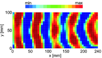
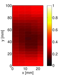
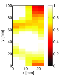
In the first case (empty waveguide), the results showed an expected result: at higher frequencies, i.e., at 5 GHz and up, the waveform inside the waveguide is close to the waveform produced by a line source. At lower frequencies, where the waveguide is electrically smaller, the reflections from the edges start to affect the field distributions, making them more complicated. See Fig. 4a for a snapshot of the measured time-harmonic electric field distribution at the frequency 5.85 GHz. Some reflections naturally still occur (mainly from the absorbers), but it is clear that the wave inside the waveguide resembles a cylindrical wave emanating from the point mm, mm.
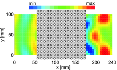
In the second case (reference object inside the waveguide), the results were again as expected: at the higher frequencies, where it makes sense to compare the field distributions, the wavefronts emanating from the source are strongly reflected at the front boundary of the reference object. The field is seen to “split” in the center and move up or down along the reference object side. See Fig. 4b for a snapshot of the measured time-harmonic electric field distribution at the frequency 5.85 GHz.
In the third case (the reference object and the transmission-line network inside the waveguide) the field pattern on the source side is seen to be well preserved (as compared to Fig. 4a) in a certain frequency band around 5.85 GHz. Also, at the backside of the network, some field is propagating. At the position of the network (which encompasses the reference object), no field is measured, since the fields are confined inside the transmission lines. See Fig. 4c for a snapshot of the measured time-harmonic electric field distribution at the frequency 5.85 GHz.
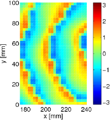
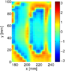
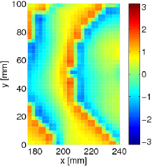
To further study the differences between the situations with and without the network, the phase distributions, calculated from the measured complex field data, are shown in Fig. 5, plotted only in the area between the reference object/network and the feed probe, i.e., in the area mm … mm. As compared to the empty waveguide (Fig. 5a), the case with the bare reference object, Fig. 5b, looks very different. This is due to the strong reflections from the front edge of the reference object. When the transmission-line network is placed inside the waveguide, together with the reference object, we see that the resulting phase distribution again is close to the one in Fig. 5a.
A more illustrative measure for the operation of the network is to compare the absolute value of the field behind the reference object with and without the network in place (i.e, in the area mm … mm). These results are shown in Fig. 6a and Fig. 6b, for the case without the network and with the network, respectively. As demonstrated by Fig. 6, the field amplitude behind the reference object is strongly suppressed (as compared to the field amplitude in front of this object). With the transmission-line network in place, the field amplitude behind the reference object/network is practically the same as in front.
The size of the network in this example case is comparable to the wavelength, so the inherent difference of the phase velocities between the wave propagating inside the network and the wave in free space, results in a change, or distortion of the impinging cylindrical waveform, as can be seen from Fig. 6b. The reasons for this difference in the phase velocity are discussed in Ref. Alitalo_cloak_TAP . Also, as the sharp edges of the square-shaped network are close to the measured area, scattering from these edges distorts the waveform. Note that the previously simulated “cloak slab” Alitalo_cloak_TAP was much wider than the network measured here.
To obtain efficient cloaking, i.e., to preserve the waveform of the incident wave both in front and behind the object (to reduce the total scattering cross section), one clearly needs to use a cloak which is electrically small enough and which does not have strong irregularities in its shape, not to cause significant forward scattering. It is also possible to use an electrically large cloak, dimensions of which are properly designed for a specific frequency range so that the desired reduction of the forward scattering is achieved Alitalo_cloak_TAP . When the incidence angle of the impinging radiation is not known, the cloak naturally needs to be symmetric, i.e., cylindrical in the two-dimensional case or spherical in the three-dimensional case Alitalo_cloak_TAP ; Alitalo_cloak_iWAT08 . Also, what is important in the case when the angle of the incident radiation is not known, the transmission-line network needs to be isotropic in the frequency range where most efficient cloaking is needed, i.e., the network period must be small enough as compared to the wavelength, as e.g. in the cylindrical cloak studied in Ref. Alitalo_cloak_iWAT08 .
V Conclusions
We have presented a prototype of a previously proposed and designed transmission-line network for cloaking purposes. In this paper we have demonstrated the benefits of this approach, such as the simple manufacturing, and confirm by measurements the predicted impedance matching with free space and the resulting field propagation through such a network (with a periodic array of metallic rods placed between the transmission lines of the network). The results are compared with a measurement of an empty measurement cell and with a measurement of the periodic array of metallic rods, effectively behaving as an impenetrable wall at the frequencies of interest.
Acknowledgements
This work has been partially funded by the Academy of Finland and TEKES through the Center-of-Excellence program and partially by the European Space Agency (ESA–ESTEC) contract no. 21261/07/NL/CB (Ariadna program). The authors wish to thank Mr. E. Kahra and Mr. L. Laakso for valuable help with manufacturing of the prototype and with building of the measurement setup. P. Alitalo acknowledges financial support by the Finnish Graduate School in Electronics, Telecommunications, and Automation (GETA), Tekniikan Edistämissäätiö (TES), and the Nokia Foundation.
References
- (1) A. Al and N. Engheta, Achieving transparency with plasmonic and metamaterial coatings, Phys. Rev E 72 (2005) 016623.
- (2) U. Leonhardt, Optical conformal mapping, Science 312 (2006) 1777–1780.
- (3) J.B. Pendry, D. Schurig, and D.R. Smith, Controlling electromagnetic fields, Science 312 (2006) 1780–1782.
- (4) D. Schurig, J.J. Mock, B. J. Justice, S.A. Cummer, J.B. Pendry, A.F. Starr, and D.R. Smith, Metamaterial electromagnetic cloak at microwave frequencies, Science 314 (2006) 977–980.
- (5) M. Kerker, Invisible bodies, J. Opt. Soc. Am. 65 (1975) 376–379.
- (6) H. Chew and M. Kerker, Abnormally low electromagnetic scattering cross sections, J. Opt. Soc. Am. 66 (1976) 445–449.
- (7) A. Sihvola, Properties of dielectric mixtures with layered spherical inclusions, Microwave Radiomet. Remote Sens. Appl. (1989) 115–123.
- (8) P.-S. Kildal, A. A. Kishk, and A. Tengs, Reduction of forward scattering from cylindrical objects using hard surfaces, IEEE Trans. Antennas Propagat. 44 (1996) 1509–1520.
- (9) A. Greenleaf, M. Lassas, G. Uhlmann, On nonuniqueness for Calderon’s inverse problem, Math. Res. Lett. 10 (2003) 685–693.
- (10) P. Alitalo, O. Luukkonen, L. Jylhä, J. Venermo, and S. A. Tretyakov, Transmission-line networks cloaking objects form electromagnetic fields, IEEE Trans. Antennas Propagat. 56 (2008) 416-424.
- (11) P. Alitalo and S. Tretyakov, Cylindrical transmission-line cloak for microwave frequencies, in: Proceedings of the 2008 IEEE International Workshop on Antenna Technology (2008) 147-150.
- (12) P. Alitalo, O. Luukkonen, J. Vehmas, and S. A. Tretyakov, Impedance-matched microwave lens, IEEE Antennas and Wireless Propagation Lett., in press (published online).
- (13) S. Maslovski, S. A. Tretyakov, and P. Alitalo, Near-field enhancement and imaging in double planar polariton-resonant structures, Journal of Applied Physics 96 (2004) 1293-1300.