Restrictions on modeling spin injection by resistor networks
Abstract
Because of the technical difficulties of solving spin transport equations in inhomogeneous systems, different resistor networks are widely applied for modeling spin transport. By comparing an analytical solution for spin injection across a ferromagnet - paramagnet junction with a resistor model approach, its essential limitations stemming from inhomogeneous spin populations are clarified.
Conventional electronics is based on a single parameter of electron, its charge. Therefore, electronics deals only with electron trajectories. It does not involve electron spin, its internal degree of freedom. The new paradigm of spin-based electronics, or spintronics, is based on active involvement of electron spin in transport and optical phenomena, and on employing electron spin for both information processing and information storage. During the last decade, semiconductor spintronics developed into a wide and diversified field. Early review papers Prinz ; Wolf were followed by more recent surveys covering specific scientific problems and technological perspectives of this rapidly developing field Awsch02 ; Gregg ; Ohno ; GanPr ; Silsbee ; Zutic ; Schmidt ; Tserkov ; Engel ; Flatte ; Jake ; HansonRMP ; Sinitsyn ; Dietl ; Bratk . There exists close connection between the recent work on electric spin manipulation in low-dimensional systems and the previous work on anomalous Hall effect KarLut , electric dipole spin resonance EDSR , optical orientation OptOr and photogalvanic effect IvPik ; BelinStu in three-dimensional systems. Strong impetus for semiconductor spintronics was given by the discovery of giant magnetoresistance in metallic systems Baibich ; Binash and by its impressing practical applications.
Spin injection from ferromagnetic sources into paramagnetic media is believed to be an important part of the new phenomena and applications in the field of the spin-polarized electron transport. The concept of a field effect spin transistor Datta served as one of the stimuli. Successful experiments on spin injection into superconductors TedMes and normal metals JohnSil were very promising, and theoretical work supported reliability of the idea AronPik ; Aronov ; JohnSil87 ; Son ; Valet ; Hershfield . Successful detection of the floating potential (spin-e.m.f., electromotive force Silsbee80 ) at a ferromagnetic probe became an independent confirmation of efficient spin injection. Meantime, the methods that resulted in a remarkable success in spin injection from ferromagnetic metals into paramagnetic metals turned inefficient as applied to the spin injection from ferromagnetic metals into semiconductors. Spin injection at the level of only about 1% was reported Hammar99 ; Gardelis , and persuasiveness of the results was disputed Monson ; Wees . Absence of any measurable spin-e.m.f. also indicated that the concentration of the electrically injected nonequilibrium spins was vanishingly small Filip .
Inefficiency of a “perfect” contact between a ferromagnetic metal and a semiconductor as a spin emitter, that seemed puzzling, found its natural explanation in the framework of the conductivity mismatch concept Schmidt00 . The next step was proposing resistive spin selective contacts, like tunnel or Schottky barriers, as spin sources Rashba00 . The underlying physics is as follows. Elements of the circuit with small effective resistances are “soft”, i.e., the concentration of nonequilibrium spins in them adjusts to the regime imposed by the elements with large effective resistances. E.g., a ferromagnetic metal connected to a semiconductor by a “perfect” (zero-resistance) contact is such a soft element. Inside it the diffusive current of minority spins enhances their Ohmic current, while the diffusive current of majority spins partly compensates their Ohmic current. As a result, electric current across the contact becomes nearly spin unpolarized, hence, good metal is a poor spin emitter. However, both the metal and semiconductor become “soft” elements if the resistance of a barrier inserted between them is larger than their effective resistances. Under these conditions, spin injection is controlled by spin selectivity of the barrier, i.e., by the difference in its resistances for up- and down-spin electrons.
More detailed diffusive theories of spin injection confirmed this concept FertJaf ; Rashba02 , and it was generalized for ballistic transport across spin valves Kravch ; Jiang ; Rashba03 and for optimization of Schottky barriers Albrecht . It also explained dramatic inefficiency of low-resistance contacts, and early observations of spin injection from STM tips Alvorado , resonant double barriers Ohno98 , and Schottky barriers Monsma . Finally, it allowed increasing spin injection coefficients from ferromagnetic metals into semiconductors to the level of dozens of percents nearly immediately Zhu ; Hammar01 ; Hanbicki ; Motsnyi ; Kreuser ; Hu . Resistive contacts became instrumental even in increasing the metal-to-metal spin injection Jedema , i.e., in a system where no considerable conductivity mismatch could be anticipated. Actually, the conductivity mismatch (or “bottlenecking”) can already been found in some previous theories JohnSil87 ; Hershfield , but importance of it has not been properly recognized then.
Different approaches for overcoming the suppression of spin injection by conductivity mismatch are based on developing semimagnetic semiconductors Oester99 ; Osipov ; Fiedr99 ; Ohno99 ; Jonker00 ; Dietl00 and half-metals Pick01 ; Park02 ; Mav04 for spin emitters.
The concepts discussed above are based on the solutions found for planar, i.e., one-dimensional, geometry. It is a price for deriving the results that are exact. The limitations of this geometry are very restricting. Geometry of real experimental systems is much more complicated, and it is well known that specific geometry around contacts influences spin injection Raichev . Any deviation from planar geometry requires applying either approximate TakaMa or numerical methods JohnBY . Even for a strictly planar geometry only a F-N-junction, i.e., a junction between a ferromagnet and a normal conductor (paramagnetic metal or semiconductor) can be easily solved. Solving a diffusive F-N-F valve is elementary but cumbersome. Using a proper calculational technique allows simplifying the procedure essentially Rashba02 , but a discrepancy in the results still persisting reflects existence of technical problems.
Under such conditions, in designing devices and analyzing their behavior in different regimes various resistor network schemes are widely used. An excellent example of exploiting such an approach can be found in the review paper by Schmidt Schmidt . Nevertheless, a general question exists: in which extent applying such network schemes to the geometries that can be solved exactly proves the consistency of the network approach? Also, which level of accuracy can be expected and which factors influence it? It is shown in what follows that for a F-N-junction in a linear (Ohmic) regime the spin injection coefficient and junction resistance cannot be described in a framework of a single resistor network scheme.
Spin injection coefficient is defined as
| (1) |
where and are the currents of spin-up and spin-down electrons, respectively, at the center of the junction (F-N interface), and is the total electric current. For a resistive F-N-contact, the expression for is well known Hershfield ; Rashba00
| (2) |
where
| (3) |
Here and are effective (diffusive) resistances of the ferromagnet and the normal conductor
| (4) |
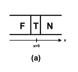
and are spin diffusion lengths in them, and and are the conductivities of spin-up and spin-down electrons, respectively, in the ferromagnet. Then is the total conductivity of the ferromagnet, describes spin polarization in the bulk of the ferromagnet, and is the conductivity of the N-conductor. As distinct from these bulk parameters, and are the conductivities of the tunnel barrier for spin-up and spin-down electrons, respectively, with and . Evidently, the ratio measures spin selectivity of the resistive contact. When deriving Eq. (1) it was assumed that the contact is spin conserving, i.e., and are continuous functions of at , FIG. 1(a). It is seen from Eq. (3) that has a meaning of an effective resistance of the contact, that together with and makes the total effective resistance of the junction . For , equation for reduces to Son ; Schmidt00 .
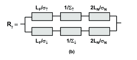
Schmidt et al. Schmidt01 and Jonker et al. Jonker03 proposed simple and appealing resistor networks for systems including magnetic and normal conductors, see FIG. 1(b). Despite the fact that both networks are “topologically equivalent” and look as nearly identical, they were proposed for different systems. Therefore, the meaning of the resistances in these networks is rather different. The network of Ref. Schmidt01, was proposed for a F-N-F spin valve with infinite spin flip time in the normal region, , and is unrelated to the basic subject of the present paper. On the contrary, the network of Ref. Jonker03, was proposed for spin injection across a F-N-junction and is an excellent candidate for comparing with the results derived for diffusive regime.
The network of Ref. Jonker03, , see FIG. 1(b), consists of two channels, each of them for a single component of electron spin, . Inside each channel, effective resistances of F- and N-conductors and of the barrier contribute in series as
| (5) |
Because the ratio of the currents across these channels equals , one recovers Eq. (2) after simple algebra. Therefore, the resistor network of FIG. 1(b) describes spin injection coefficient perfectly, as it was already stated by Jonker et al. Jonker03 . Next physical quantity of interest is the electrical resistance of a F-N-junction. For the resistor network of FIG. 1(b) it equals
| (6) |
Electrical resistance of a diffusive F-N-junction was found in Ref. Rashba00, , and detailed derivation was provided in Ref. Rashba02, . However, because this resistance is critical for our final results, we outline here the basic guidelines for the derivation. On both sides of the junction, inside the F- and N-conductors, electrochemical potentials of up- and down-spin electrons obey the standard drift-diffusion equations JohnSil87 ; Son ; Valet ; Hershfield . The contact conductivities of the F-N-interface, , are defined by the boundary condition
where are current densities of up- and down-spin electrons, respectively. The superscripts N and F in indicate that the corresponding potentials should be taken at the F- and N-sides of the interface, respectively. This boundary condition implies the continuity of at , what is tantamount to spin conservation at the F-N-interface. We note that Eq. (2) was derived under the same conditions and by the same procedure.
Under these conditions, the F-N-junction resistance , excluding nominal resistances of the F- and N-conductors, equals Rashba00 ; Rashba02
| (7) | |||||
Remarkably, the resistance of a tunnel barrier appearing here differs from the effective resistance of Eq. (3). Second term in (7) represents the nonequilibrium part of that is always positive. It vanishes when and nonequilibrium spin populations cease to exist; under these conditions . F-N-junction acquires a finite resistance, , even for a zero-resistance barrier, . We note that throughout this paper the term “resistive contact” implies .
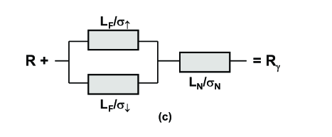
Comparing Eqs. (6) and (7) shows that . They are related by the equation
| (8) |
It shows that , and and differ by the diffusive resistances of the ferromagnet, , and the normal conductor, [of which the former does not coincide with of Eq. (4)]. Eq. (8) is shown graphically in FIG. 1(c).
It is seen from Eq. (8) that the difference between and is a general phenomenon. It is related to spin diffusion in F- and N-regions rather than to a tunnel barrier separating them. Therefore, to uncover the underlying physics we consider a transparent barrier () when Eqs. (6) and (7) are essentially simplified. It follows from Eq. (7) that in this case electrical resistance of the junction equals
| (9) |
Therefore it vanishes, , whenever one of the spin diffusion lengths, either or , vanishes. It is a result that is anticipated from simple physical arguments. Indeed, when , electrochemical potentials of up- and down-spin electrons, , are continuous at
| (10) |
When one of the diffusion lengths, say , vanishes, electron spins are in equilibrium in the whole N-region, hence, for . Then it immediately follows from Eq. (10) that , and this suggests that in the whole F-region, . Therefore, spin equilibrium on one side of the junction maintains spin equilibrium also on the other side of it, and second term in Eq. (7) always vanishes in the absence of spin nonequilibrium. Under these conditions, .
One can check by inspection that of Eq. (6) does not obey this requirement, and it vanishes only when both spin diffusion lengths vanish, . Presence of second and third terms in the left hand side of Eq. (8) reflects this critical difference in the properties of and . Therefore, the network of FIG. 1(b) provides perfect description of spin injection coefficient , but cannot provide a consistent description of the junction resistance . When barrier resistance is high, describes consistently the leading term in . Inaccuracy in the next terms, originating from spin imbalance in the bulk, depends on specific parameter values.
In conclusion, it is instructive to compare two-channel resistor models of spin injection with the Mott’s two-channel model of spin transport in ferromagnetic metals Mott36 . In the latter model, scattering influences only the mobilities of the carriers with different spins. Because of homogeneity of the system, scattering does not produce spin imbalance and nonequilibrium spin populations. That is why the conductivities and are well defined. On the contrary, nonequilibrium spin populations are central for the spin injection problem, and all processes responsible for spin relaxation critically influence spacial distribution of these populations. Two-channel resistor models, at least in their simplest realizations, are not properly fit for describing the effect of inhomogeneous populations.
References
- (1) Prinz G. A. 1998 Science 282 1660
- (2) Wolf S. A., Awschalom D. D., Buhrman R. A., Daughton J. M., von Molnar S., Roukes M. J., Chtchelkanova A. Y., and Treger D. M. 2001 Science 294 1488
- (3) Awschalom D. D., Loss D., and Samarth N. (2002) Semiconductor Spintronics and Quantum Computation (Springer, Berlin)
- (4) Gregg J. F., Petej I., Jouguelet E., and Dennis C. 2002 J. Phys. D: Appl. Phys. 35 R121
- (5) Semiconductor Spintronics, Special issue of: Semicond. Sci. Technol., ed. by H. Ohno, 2002, 17, No 4
- (6) Ganichev S. D. and Prettl W. 2003 J. Phys.: Condens. Matter, 15, R935-983
- (7) Silsbee R. H. 2004 J. Phys.: Cond. Matter 16 R179
- (8) Žutić I, Fabian J., and Das Sarma S. 2004 Rev. Mod. Phys. 76 323
- (9) Schmidt G. 2005 J. of Phys. D: Applied Physics 38 R107
- (10) Tserkovnyak Y., Brataas A., Bauer G. E. W., Halperin B. I. 2005 Rev. Mod. Phys. 77 1375
- (11) Engel H.-A., Rashba E. I., and Halperin B. I., in: Handbook of Magnetism and Advanced Magnetic Materials, Vol. 5 (Wiley, Chichester, 2007), p. 2858; arXiv:cond-mat/0603306.
- (12) Flatte M. E. 2007 IEEE Trans. on Electron Devices 54 907
- (13) Taylor J. M., Petta J. R., Johnson A. C., Yacoby A., Marcus C. M., Lukin M. D. (2007) Phys. Rev. B 76 035315
- (14) Hanson R., Kouwenhoven L. P., Petta J. R., Tarucha S., Vandersypen L. M. K. 2007 Rev. Mod. Phys. 79, 1217
- (15) Sinitsyn N. A. 2008 J. Phys.: Cond. Mat. 20, 023201
- (16) Dietl T. 2007 in: Lecture Notes 712 (Springer, Berlin) p. 1; arXiv:0801.0145
- (17) Bratkovsky A. M. 2008 Rep. Prog. Phys. 71 026502
- (18) Karplus R. and Luttinger J. M. 1954 Phys. Rev. 95 1154
- (19) Rashba E. I. and Sheka V. I., in Landau Level Spectroscopy, edited by G. Landwehr and E. I. Rashba, 1991 (North-Holland, Amsterdam), p. 131.
- (20) Optical Orientation, ed. by F. Meier and B. P. Zakharchenya, 1984 (North-Holland, Amsterdam)
- (21) Ivchenko E. L. and Pikus G. E. 1978 Pis’ma Zh. Eksp. Teor. Fiz. 27 640 [JETP Lett. 27 604].
- (22) Belinicher V.I. and Sturman B.I. 1980 Sov. Phys. Usp. 23 199 [Usp. Fiz. Nauk 130 415]
- (23) Baibich M. N., Broto J. M., Fert A., Van Dau N. F., Petroff F., Etienne P., Creuzet G., Friederich A. , and Chazelas J. 1988 Phys. Rev. Lett. 61, 2472
- (24) Binash G., Grünberg P., Saurenbach F., and Zinn W. 1989 Phys. Rev. B 39 4828
- (25) Datta S. and Das B. 1990 Appl. Phys. Lett. 56 665
- (26) Tedrow P. M. and Meservey R. 1973 Phys. Rev. B 7 318
- (27) Johnson M. and Silsbee R. H. 1985 Phys. Rev. Lett. 55 1790
- (28) Aronov A. G. and Pikus G. E. 1976 Fiz. Tekh. Poluprovodn. 10 1177 [1976 Sov. Phys. Semicond. 10 698]
- (29) Aronov A. G. 1976 Pis’ma Zh. Eksp. Teor. Fiz. 24 37 [1976 JETP Lett. 24 32]
- (30) Johnson M. ans Silsbee R. H. 1987 Phys. Rev. B 35 4959
- (31) van Son P. C., van Kampen H., and Wyder P. 1987 Phys. Rev. Lett. 58 2271
- (32) Valet T. and Fert A. 1993 Phys. Rev. B 48 7099
- (33) Hershfield S. and Zhao H. L. 1997 Phys. Rev. B 56 3296
- (34) Silsbee R. H. 1980 Bull. Magn. Res. 2 1984
- (35) Hammar P. R., Bennett B. R., Yang M. J., and Johnson M. 1999 Phys. Rev. Lett. 83, 203
- (36) Gardelis S., Smith C. J., Barnes C. H. W., Linfield E. H., and Ritchie D. A. 1999 Phys. Rev. B 60 7764
- (37) Monson F. G., Tang H. X., and Roukes M. L. 2000 Phys. Rev. Lett. 84 5022
- (38) van Wees B J 2000 Phys. Rev. Lett. 84 5023
- (39) Filip A. T., Hoving B. H., Jedema F. J., van Wees B. J., Dutta B., and Borghs S. 2000 Phys. Rev. B 62 9996
- (40) Schmidt G., Ferrand D., Molenkamp L. W., Filip A. T., and van Wees B. J. 2000 Phys. Rev. B 62 R4790
- (41) Rashba E. I. 2000 Phys. Rev. B 62 R16267
- (42) Fert A. and Jaffrès H. 2001 Phys. Rev. B 64 184420
- (43) Rashba E. I. 2002 Euro. Phys. Journal B 24 513
- (44) Kravchenko V. Ya. and Rashba E. I. 2003 Phys. Rev. B 67 121310(R)
- (45) Jiang X., Wang R., van Dijken S., Shelby R., Macfarlane R., Solomon G. S., Harris J., and Parkin S. S. P. 2003 Phys. Rev. Lett. 90 256603
- (46) Rashba E. I. 2003 Phys. Rev. B 68 241310(R)
- (47) Albrecht J. D. and Smith D. L. 2003 Phys. Rev. B 68 035340
- (48) S. F. Alvorado 1995 Phys. Rev. Lett. 75 513
- (49) Ohno H. 1998 Science 281 951
- (50) Monsma D. J., Flutters R. and Lodder J. C. 1998 Science 281 407
- (51) Zhu H. J., Ramsteiner M., Kostial H., Wassermeier M., Schönherr H.-P., and Ploog K. H. 2001 Phys. Rev. Lett. 87 016601
- (52) Hammar P. R. and Johnson M. 2001 Appl. Phys. Lett. 79, 2591
- (53) Hanbicki A. T., van ’t Erve O. M. J., Magno R., Kioseoglou G., Li C. H., Jonker B. T., Itskos G., Mallory R., Yasar M., and Petrou A. 2003 Appl. Phys. Lett. 82 4092
- (54) Motsnyi V. F., Safarov V. I., De Boeck J., Das J., Van Roy W., Goovaerts E., and Borghs G. 2002 Appl. Phys. Lett. 81 265
- (55) Kreuzer S., Moser J., Wegscheider W., Weiss D., Bichler M., and Schuh D. 2002 Appl. Phys. Lett. 80 4582
- (56) Hu C.-M., Nitta J., Jensen A., Hansen J. B., Takayanagi H., Matsuyama T., Heitmann D., and Merkt U. 2002 J. Appl. Phys. 91 7251
- (57) Jedema F. J., Heersche H. B., Filip A. T., Baselmans J. J. A., and van Wees B. 2002 Nature 416 713
- (58) Oestreich M., J. Hübner, D. Hägele, P. J. Klar, W. Heimbrodt, W. W. Rühle, D. E. Ashenford, and B. Lunn 1999 Appl. Phys. Lett. 74 1251
- (59) Osipov V. V., N. A. Viglin, and A. A. Samokvalov 1998 Phys. Lett. A 247 353
- (60) Fiederling R., M. Keim, G. Reuscher, W. Ossau, G. Schmidt, A. Waag, and L. W. Molenkamp 1999 Nature 402 787
- (61) Ohno Y., D. K. Young, B. Beschoten, F. Matsukara, H. Ohno, and D. Awschalom 1999 Nature 402 790
- (62) Jonker B. T., Y. D. Park, B. R. Bennett, H. D. Cheong, G. Kioseoglou and A. Petrou 2000 Phys. Rev. B 62 8180
- (63) Dietl T., H. Ohno, F. Matsukura, J. Cibert, and D. Ferrand 2000 Science 287 1019
- (64) Pickett W. E. and J. Moodera 2001 Phys. Today, May 2001, p. 39
- (65) Parker J. S., S. Watts, P. G. Ivanov, and P. Xiong 2002 Phys. Rev. Lett. 88 196601
- (66) Mavropoulos Ph., K. Sato, R. Zeller, P. H. Dederichs, V. Popescu, and H. Ebert 2004 Phys. Rev. B 69 054424
- (67) Raichev O. E. and Debray P. 2002 Phys. Rev. B 65 085319
- (68) Takahashi S. and Maekawa S. 2003 Phys. Rev. B 67 052409
- (69) Johnson M. and Byers J. 2003 Phys. Rev. B 67 125112
- (70) Schmidt G., Molenkamp L. W., and Bauer G. W. 2001 Materials Science and Engineering C 15 83
- (71) Jonker B. T., Erwin S. C., Petrou A., and Petukhov A. G. 2003 MRS Bulletin 28 740
- (72) Mott N. F. 1936 Proc. Royal Soc. (London) A 153 699
 |
|
 |
 |