Nanoengineering of a Negative-Index Binary-Staircase Lens for the Optics Regime
Abstract
We show that a binary-staircase optical element can be engineered to exhibit an effective negative index of refraction, thereby expanding the range of optical properties theoretically available for future optoelectronic devices. The mechanism for achieving a negative-index lens is based on exploiting the periodicity of the surface corrugation. By designing and nanofabricating a plano-concave binary-staircase lens in the InP/InGaAsP platform, we have experimentally demonstrated at 1.55 m that such negative-index concave lenses can focus plane waves. The beam propagation in the lens was studied experimentally and was in excellent agreement with the three-dimensional finite-difference time-domain numerical simulations.
pacs:
42.70.Qs, 41.20.Jb, 73.20.Mf, 78.20.CiThe field of metaphotonics shalaev_np07 ; veselago06 ; pendry96 ; pendry99 ; PhysRevB.62.10696 ; Gralak:00 ; luoprb02 ; casseapl07 ; gmachl07 , or the merging of metamaterials veselago68 and photonics Joannopoulos95 ; yablonovitch87 ; sajeevjohn87 , has opened doors to a plethora of unusual electromagnetic properties, such as negative refraction RAShelby04062001 ; parimi03 , cloaking D.Schurig11102006 and optical data storage kosmas_nat_07 , that cannot be obtained with naturally occurring materials. The holy grail of manufacturing these artificial photonic metamaterials structures, is to manipulate light at the nanoscale level for optical information processing and high-resolution imaging. In this paper we demonstrate how a binary-staircase optical element can be tailor-made to have an effective negative refractive index, and thus bringing an alternative approach to negative-index optical elements.
Here we consider a binary-staircase type of lens alda05 , which consists of a sequence of zones configured as flat parallel steps each having an annular shape. The binary-staircase lens is a plano-concave lens. Focusing by plano-concave lenses enoch03 ; parazzoli04 were realized in 2D and 1D photonic crystals vodo:201108 ; vodo:084104 . Proof-of-concept experiments which demonstrate negative refraction in a plano-concave grating lens have been realized earlier by our group in the microwave regime luopt07 . However the plano-concave lens used in the microwave range consisted of an assembly of commercial alumina bars, placed in a parallel-plate waveguide, which are not suitable for integration in optoelectronic circuits.
Geometrical parameters of the binary-staircase lens were determined by considering the transverse size of the lens, the focal length, wavelength of the incoming radiation, the index of the material used to fabricate the lens itself and mainly the surface periodicity. The actual lens has been nanofabricated by a combination of electron beam lithography and reactive ion etching in an InP/InGaAsP heterostructure. Subsequently, the focusing properties of the device were experimentally verified using a scanning probe optical technique. Three-dimensional (3D) finite-difference time-domain (FDTD) simulations have been used to further study the beam propagation in the lens. The FDTD simulations were in excellent agreement with the experimental results.
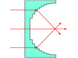
We use a surface modification scheme to alter the index of refraction of the medium luopt07 ; huang:013824 . An incident wave impinging on a smooth surface with incident angle larger than the critical angle will be totally reflected. However a proper surface grating will allow the wave to be transmitted. This is equivalent to give the incident wave a transverse momentum kick. In the case that the grating period is much smaller than the incident wavelength, an effective refractive index can be used to describe the refraction at the modified surface. For a binary-staircase lens with a plano-concave shape as shown in Fig. 1, this effective index is related to the bulk refractive index of the medium by luopt07
| (1) |
where ‘’ is a fixed step length along the optical axis (or surface periodicity) and is the free space wavelength (with ). The number of steps or zones is then , where is the transverse size of the binary-staircase lens. The focal length is calculated by using the formula . To obtain a good focus, (Abbe’s diffraction limit). In the present case, nm and was chosen as 450 nm with 3.231 for the transverse electric (TE) modes and 3.216 for the transverse magnetic (TM) modes. has been chosen as an arbitrary value in the vicinity of . 11, so that reads 10 m. Thus is 0.2133 and 0.2889 for TE and TM modes, respectively.
The fabrication platform consisted of a 400 nm InGaAsP core layer on an InP substrate with a 200 nm InP top cladding layer. The waves are trapped and propagate within the core layer plane with an effective permittivity of 3.231 (TE modes) and 3.216 (TM modes). The final structure for optical measurements consisted of three sub units (shown in Fig. 2(a)): (i) a 0.5 mm long waveguide, laterally tapered, having 5 m wide trenches on each side; The taper starts at a distance of 100 m from the edge of the waveguide, with a core width varying from 5 m to 10 m. (ii) Binary-staircase plano-concave lens with 10 zones on the optical axis, having a step height of 450 nm and a transverse size of 10 m, located at a distance of 5 m from the tapered end of the waveguide (shown in Fig. 2(b)). (iii) And finally an open cavity (semi-circle juxtaposed to a 20 m 20 m square) at the end of the binary-staircase lens.
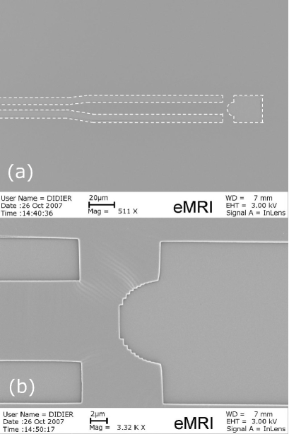
An analogue structure, having the same geometrical dimensions but bearing no steps (or zones), was fabricated. The purpose of the analogous design was to prove that the periodicity of the steps are decisive structure elements to realizing a negative-index prototype. The structures were written using electron beam lithography on polymethylmethacrylate (PMMA) resist. Pattern transfers to a silicon nitride working mask and subsequently to the InP/InGaAsP layers were achieved with a reactive ion etching (RIE) method.
In the characterization experiment, a continuous wave tunable semiconductor laser (1550 nm–1580 nm) was used as the input light source. The laser light was coupled into the cleaved end of the input waveguides using a monomode lensed fiber (working distance 14m and FWHM 2.5 m in air) mounted on a five-axis positioning stage. An infrared (IR) camera (Hamamatsu Model C2741) connected to a microscope port aids the initial alignment to optimize the IR light coupling from the optical fiber to the waveguide. In the FDTD simulation, a 10 m wide plane parallel, Gaussian beam was chosen as incident field for the grating lens. In the actual sample, the 5 m wide input facet of the waveguide was inversely tapered to 10 m width (see Fig. 2(a)) so that the propagating Gaussian beam is expanded sufficiently inside the guiding channel before reaching the device end. The planar wavefront after emerging from the binary-staircase lens is expected to focus in the air cavity.
A tapered fiber probe (250 nm aperture diameter) metallized with a thin chromium and gold layer was raster scanned just above the sample surface. The output end of the fiber probe was connected to nitrogen cooled germanium detector (North Coast Scientific Corp. Model EO-817L). Additionally, a typical lock-in amplifier was utilized to optimize the detection scheme. Scanning the fiber tip at a constant height about 500 nm above the sample surface allowed us to probe the optical intensity distribution over a grid of points spanning m2 area. The reconstructed image is shown in Fig. 3(a).
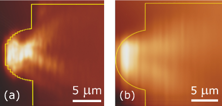
Intensity distribution near the cavity center clearly shows the light focusing from the binary-staircase lens. Identical focusing fingerprints were observed when the experiment was repeated over a range of wavelengths varying from 1510 nm to 1580 nm. Another controlled experiment was performed where the binary-staircase lens was replaced by an analogous structure (having the same geometrical features) with no steps. In the latter case, as shown in Fig. 3(b), no beam focusing was observed. Nevertheless we can distinguish a bright spot near the device’s edge, which is attributed to a sudden beam divergence as it propagates into open space from initial confinement in the InGaAsP core waveguide layer (diffraction).
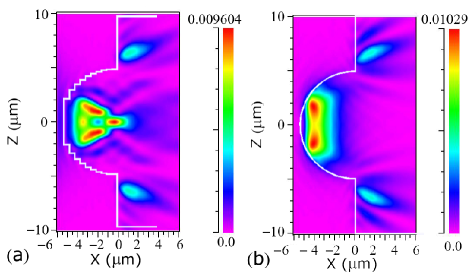
The 3D FDTD simulations were performed using perfectly matched layer boundary conditions that minimize reflections at the edges. The chosen input field excitation for the FDTD simulation was a TE polarized Gaussian beam which closely resembles the beam shape of the fiber source in actual experiment. The energy density of the propagating H-field was mapped at different plane heights. Figures 4(a) and 4(b) shows the simulated H-field density of the binary-staircase lens and the analogue structure at about 800 nm above the center of the core layer, respectively.
The traditional metamaterials structures are composed of arrays of split ring resonators and metal wires. This type of metallic structures, which operates under resonance, becomes lossy at optical frequencies due to the inherent imaginary part of the metal’s permittivity. The purely dielectric system, such as the one mentioned in this letter, is free from these drawbacks and thus has low intrinsic material loss, which is a clear-cut advantage for optical frequency operations. Extrinsic losses in the binary-staircase dielectric structure itself arise solely from the imperfections in the fabrication (e.g. surface and sidewall roughness).
We have experimentally designed a binary-staircase optical element having an effective negative index of refraction, whereby the surface periodicity of the structure acted as the tunable parameter for controlling the sign change of the refractive index. The beam propagation in the plano-concave lens was simulated using in-house 3D FDTD codes. Based on the design and simulations, we have nano-engineered a prototype structure in an InP/InGaAsP heterostructure tailored for the 1.55 m wavelength, where indium phosphide (InP) is a natural starting fabrication platform for wholesale integration of passive and active devices for a complete system-on-a-chip at this frequency. Characterization of the prototype with a near-field scanning optical microscope revealed that the plano-concave binary-staircase lens can act as a convex lens and thereby focusing plane waves. No focusing is achieved if the zones are removed, reinforcing the fact the steps are the decisive structure elements. A notable aspect of our work is the extension of electromagnetic properties (that are theoretically available) of optical elements for possible integration in optoelectronic circuits.
This work was supported by the Air Force Research Laboratories, Hanscom through grant no. FA8718-06-C-0045 and the National Science Foundation through grant no. PHY-0457002. This work was performed in part at the Kostas Center for High-Rate Nanomanufacturing at Northeastern University, and Center for Nanoscale Systems, a member of the National Nanotechnology Infrastructure Network, under NSF award no. ECS-0335765.
References
- (1) V. M. Shalaev, Nat. Photonics 1, 41 (2007) and references therein.
- (2) V. G. Veselago and E. E. Narimanov, Nat. Materials 5, 759 (2006).
- (3) J. B. Pendry, A. J. Holden, W. J. Stewart, and I. Youngs, Phys. Rev. Lett. 76, 4773 (1996).
- (4) J. B. Pendry, A. J. Holden, D. J. Robbins, and W. J. Stewart, IEEE Trans. Microwave Theory Tech. 47, 2075 (1999).
- (5) M. Notomi, Phys. Rev. B 62, 10696 (2000).
- (6) B. Gralak, S. Enoch, and G. Tayeb, J. Opt. Soc. Am. A 17, 1012 (2000).
- (7) C. Luo, S. G. Johnson, J. D. Joannopoulos, and J. B. Pendry, Phys. Rev. B 65, 201104 (2002).
- (8) B. D. F. Casse, H. O. Moser, J. W. Lee, M. Bahou, S. Inglis, and L. K. Jian, Appl. Phys. Lett. 90, 254106 (2007).
- (9) A. J. Hoffman, L. Alekseyev, S. S. Howard, K. J. Franz, D. Wasserman, V. A. Podolskiy, E. E. Narimanov, D. L. Sivco and C. Gmachl1, Nat. Materials 6, 946 (2007).
- (10) V. G. Veselago, Sov. Phys. Usp. 10, 509 (1968).
- (11) John D. Joannopoulos, Robert D. Meade, and Joshua N. Winn. Photonic Crystals: Molding the Flow of Light. Princeton University Press (1995).
- (12) E. Yablonovitch, Phys. Rev. Lett. 58, 2059 (1987).
- (13) S. John, Phys. Rev. Lett. 58, 2486 (1987).
- (14) R. A. Shelby, D. R. Smith, and S. Schultz, Science 292, 77 (2001).
- (15) P. V. Parimi, W. T. Lu, P. Vodo, and S. Sridhar, Nature 426, 404 (2003).
- (16) D. Schurig, J. J. Mock, B. J. Justice, S. A. Cummer, J. B. Pendry, A. F. Starr, and D. R. Smith, Science 314, 977 (2006).
- (17) K. L. Tsakmakidis, A. D. Boardman, and O. Hess, Nature 450, 397 (2007).
- (18) J. Alda, J. M. Rico-García, J. M. López-Alonso, B. Lail, and G. Boreman, Opt. Comm. 260, 454 (2005).
- (19) S. Enoch, G. Tayeb, and B. Gralak, IEEE Trans. on Antennas and Propagation 51, 2659 (2003).
- (20) C. G. Parazzoli, R. B. Greegor, J. A. Nielsen, M. A. Thompson, K. Li, A. M. Vetter, M. H. Tanielian, and D. C. Vier, Appl. Phys. Lett. 84, 3232 (2004).
- (21) P. Vodo, P. V. Parimi, W. T. Lu, and S. Sridhar, Appl. Phys. Lett. 86, 201108 (2005).
- (22) P. Vodo, W. T. Lu, Y. Huang, and S. Sridhar, Appl. Phys. Lett. 89, 084104 (2006).
- (23) W. T. Lu, Y. J. Huang, P. Vodo, R. K. Banyal, C. H. Perry, and S. Sridhar, Opt. Express 15, 9166 (2007).
- (24) Y. J. Huang, W. T. Lu, and S. Sridhar, Phys. Rev. A 76, 013824 (2007).