Conductance through atomic point contacts between fcc(100) electrodes of gold
Abstract
Electrical conductance through various nanocontacts between gold electrodes is studied by using the density functional theory, scalar-relativistic pseudopotentials, generalized gradient approximation for the exchange-correlation energy and the recursion-transfer-matrix method along with channel decomposition. The nanocontact is modeled with pyramidal fcc(100) tips and 1 to 5 gold atoms between the tips. Upon elongation of the contact by adding gold atoms between the tips, the conductance at Fermi energy evolves from to (). Formation of a true one-atom point contact, with and only one open channel, requires at least one atom with coordination number 2 in the wire. Tips that share a common vertex atom or tips with touching vertex atoms have three partially open conductance channels at , and the symmetries of the channels are governed by the wave functions of the tips. The long 5-atom contact develops conductance oscillations and conductance gaps in the studied energy range eV, which reflects oscillations in the local density of electron states in the 5-atom linear ”gold molecule” between the electrodes, and a weak coupling of this ”molecule” to the tips.
pacs:
61.46.Km, 73.23.Ad, 73.63.Nm1 Introduction
Stable atomic point contacts and chain-like wires between metal leads constitute an intensive research field aimed at atomic-precision manipulation of mechanical and electrical properties of nanojunctions for possible use in future nanoelectronics [1, 2]. Gold nanowires have been an archetypical system; early experimental discoveries [3, 4] of stable several-atom-long wires have sparked extensive theoretical and experimental interest [5]-[23]. Along with detailed results for the dependence of conductance on the nanowire structure, early electronic structure calculations predicted also considerable chemical ”sensing activity” of these contacts [9, 10].
Gold nanowires are ideal systems to study ballistic transport in an atomic environment, since (i) the wires are shorter than the electron mean-free path and (ii) the Fermi wave length of gold is comparable to the diameter of an ultimately narrow wire (one gold atom), allowing for passage of current with one unit of the quantum conductance at energies close to . Step-wise reduction of the conductance down to upon stretching (and concomitant narrowing) of the contact is well documented in many experiments and calculations. Specifically, formation of several-atom long wires with was reported in the ground-breaking experiments in 1998 [3, 4]. Particularly in the mechanical break-junction experiment [4] formation of a one-atom point contact was attributed to the discrete jump of conductance down to . This result has been conventionally interpreted as there being just one open conductance channel (s-like channel, according to the monovalent nature of gold [5]).
This work re-iterates the fundamental question: when does a wire constitute a ”truly” one-atom point contact with only single open channel? On the basis of density-functional-theory (DFT) calculations of relaxed model structures and accompanied recursion transfer-matrix (RTM) calculations for the (intrinsic, without bias) conductance, we show that a conductance value close to the quantum unit is not a sufficient criterion to identify a ”true” atomic point contact between the leads, modeled here with two fcc(100) tips. Upon formation of the wire, configurations exist which appear to have a minimal cross-section of just one gold atom, however up to three conductance channels can be partially open to yield a total conductance . Formation of a true one-atom point contact with only one open conductance eigenchannel requires at least one atom in the wire with a coordination number of two, i.e., three atoms in a linear configuration. This way, the formation of the point contact is intimately linked to the chemical coordination of the atoms in the wire. Tips that share a common vertex atom or tips with touching vertex atoms have three partially open conductance channels at , and the symmetries of the channels are governed by the wave functions of the tips. We have also studied a long 5-atom wire (7 atoms altogether in a linear configuration) and observed that it develops conductance oscillations and conductance gaps in the studied energy range eV. This reflects oscillations in the local density of electron states in the 5-atom linear ”gold molecule” between the electrodes.
2 Method
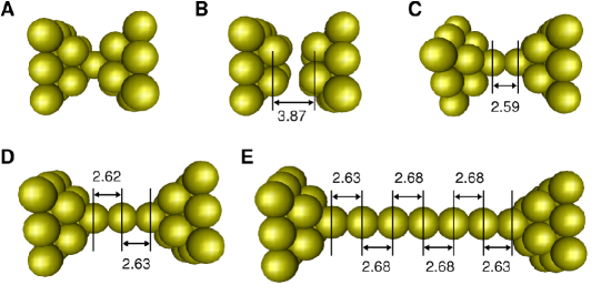
Atomic structures of the model contacts were relaxed and the electronic structure analysed by using a density-functional total-energy method based on ref. [24]. The interactions between the 5d and 6s electrons and the core electrons of gold were described by scalar-relativistic Troullier-Martins norm-conserving first-principles pseudopotentials [25] in conjunction with the Perdew-Burke-Ernzerhof (PBE) exchange-correlation potential [26]. The nanocontact is built of two fcc(100) tips with a variable number of gold atoms between the tips in the (100)-axis (z), see Fig. 1. The length of each contact was relaxed with the constrain that the atoms in the outermost layers of the tips were fixed to their lattice-terminated (x,y) positions.
For obtaining the conductance, the local part of the self-consistent Kohn-Sham potential of the DFT calculation was used in the recursion-transfer-matrix method along with the conductance eigenchannel decomposition [27, 28, 29]. The transmission of the electron propagating from one electrode to another through of the wire region is evaluated using a numerical solution of the stationary states of the Schrödinger equation. In the direction of the wire, propagation of the electrons is started from a smooth jellium potential (at -11 eV) of the lead and stopped when the bulk value of the potential is reached on the opposite lead. In the transverse direction periodic boundary conditions are used.
The conductance was calculated from the Landauer-Büttiker formula as a sum over all non-zero conductance channels
| (1) |
where are the eigenvalues of the product of transmission matrices, . Convergence of the obtained conductance values has been carefully tested with respect to number of plane waves in the transverse direction, number of atomic layers in the tips, number of points in the calculation grid into the bulk region of the lead. Finally, we have checked that the use of the local 6s-part for constructing the from the non-local self-consistent Kohn-Sham potential that includes the 5d-6s-6p angular momentum channels of the pseudopotential is a quantitatively satisfying approximation.
3 Results and discussion
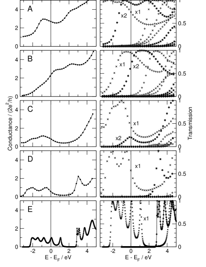
Figure 2 shows conductance versus energy (left column) and the eigenchannel decomposition (right column) for all the configurations A-E shown in Fig. 1. Table 1 summarizes the conductance values at the Fermi energy, .
-
Contact A 2.7 3 B 2.3 3 C 0.8 3 D 0.6 1 E 0.9 1
The contact A shows a local maximum in the conductance ( G0) 1 eV below . At the Fermi level the conductance is G0 and reaches a local minimum at slightly higher energies. This high value of conductance was also obtained in [18] for the same system. The eigenchannel analysis shows three partially open conducting channels. At , the transmittance of the first (non-degenerate) and second channel (doubly degenerate) are 0.75 and 0.93, respectively. Higher channels show transmittance below 0.05.
This contact provides the first example where on structural grounds one could argue that a one-atom point contact has been formed. From the point of view of the electronic structure, this is not the case. Existence of three major channels implies dominance of the tip electronic structure. As a straightforward test, we removed the central atom in structure A (see structure B in Fig. 1) and re-calculated the electronic structure, and the conductance. Three major channels remain open at and the conductance remains high, .
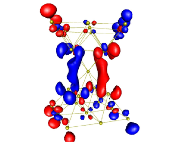
As has been noted previously [5], the degeneracy patterns of conductance channels close to Fermi energy can be related to symmetries of electronic orbitals in the contact region. Fig. 3 (left) displays the visualization of one of the doubly-degenerate occupied orbital close to (the other one is related by a 45-degree rotation). It is interesting to note that this orbital has virtually no weight around the shared vertex atom. This explains qualitatively also the insensitivity of the conductance to the removal of this atom (contact B).
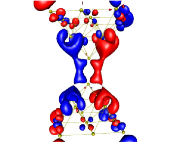
drops significantly (to 0.8 ) for contact C which consists of the tips with touching vertex atoms. The coordination number of the vertex atoms is 5. Based on the calculated conductance, one could again classify this contact as a ”one-atom point contact”. However, the eigenchannel analysis reveals three partially open channels close to . The non-degenerate channel has a transmittance of 0.4 and the doubly-degenerate channel 0.2. Fig. 3 (right) displays a visualization of the doubly-degenerate orbital close to , which forms a bonding state between the touching vertex atoms, continuing all the way to the tips.
Contact D has two maxima () at 2 eV and 0.5 eV below , and a rather low value at the Fermi level, . Only one channel remains open. It is interesting to correlate the closing of the higher channels with the decrease of the coordination number of the central atom from 5 (contact C) to 2 (contact D). Also, the single open channel at nearly closes for the region 1 - 2 eV above .
The longest studied contact E (5-atom chain) exhibits a qualitatively distinct conductance pattern: oscillations with sharp transmittance peaks for a single eigenchannel at energies eV and a wide conductance gap for eV. The sharp peaks at energies eV are due to the second eigenchannel which is doubly degenerate.
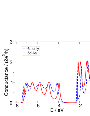
We have checked that the distinct behaviour of the contact E is not due to approximations made in building the effective local potential for the RTM calculations. A direct evidence is shown in Fig. 4 where comparison of two curves for contact E are shown. The red solid curve reproduces the data of Fig. 2 and the blue dashed curve is obtained from a RTM calculation where the is derived from 6s-only pseudopotential DFT calculation for the contact. The shapes of the two conductance curves are very similar.
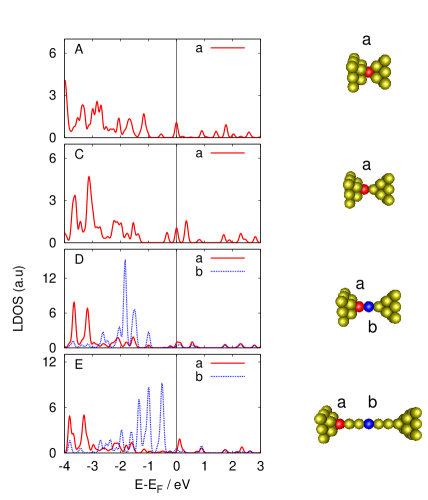
What drives the observed distinct behaviour of contact E? One may note that a qualitative change of takes place already when comparing contacts A and C: the direction of the wire axis differs from the orientation of the (100) tips. This change is correlated with the development of a broad conductance minimum at energies eV which develops further to a true conductance gap for contact E. The behaviour of contact E, a series of sharp ”resonance” peaks at eV separated by large conductance gaps from below and above, is a signature of a ”molecular” nature of the contact. This is due to two factors: (i) the local electronic structure of the longer Au chains differs markedly from that in the tips, see Figure 5, which shows well-developed oscillations in the local density of electronic states projected to the central Au atom in the wire, and (ii) mismatch of the crystal orientations between the wire and the tips ( and , respectively) causes significant back-scattering at the vertices of the tips, thus effectively decoupling the ”molecular” Au chain from the tips.
The mechanical stability of the long wire has been checked by modifying the linear five atom contact and optimizing. The modification consisted in a random shift of the wire atom coordinates in the plane perpendicular to the initial linear chain. After optimization a new isomer with lower energy has been found with the five central atoms in a zig-zag final configuration.
4 Conclusions
We have studied the conductance of different one-atom-size contacts between fcc(100) gold tips. Formation of a true one-atom point contact, with and one open eigenchannel, requires at least one atom in the wire with a coordination number of two. The long 5-atom contact develops sharp resonances and conductance gaps, signaling formation of a weakly coupled ”linear gold molecule” between the tips. The weak coupling may be due to the fact that the linear ”molecular” part of the contact has locally a axis whereas the tips are in the orientation, causing significant back-scattering at the vertex atoms. Experimental observation of this phenomenon might however be difficult due to various possible non-ideal atomic configurations of the tips. At the peaks of the resonances, the long linear chains appear to be ideal one-channel ballistic conductors with close to . The disappearance of the experimentally measured conductance for long contacts [4] is then truly due to mechanical instabilities of the wire causing breaking of the contact, and not due to inherent deterioration of conductance in long linear wires.
References
References
- [1] Serena P A, Garcia N 1997 Nanowires (Dordrecht: Kluwer)
- [2] Agraït N, Yeyati A L, van Ruitenbeek J M 2003 Phys. Rep. 377 8103
- [3] Ohnishi H, Kondo Y and Takayanagi K 1998 Nature 395 780
- [4] Yanson A I, Rubio Bollinger G, van der Brom H E, Agraït N and van Ruitenbeek J M 1998 Nature 395 783
- [5] Scheer E, Agraït N, Cuevas J C, Yeyati A L, Ludoph B, Mart n-Rodero A, Rubio Bollinger R, van Ruitenbeek J M and Urbina C 1998 Nature 394 154
- [6] Cuevas J C, Levy Yeyati A, Mart n-Rodero A, Rubio Bollinger G, Untiedt C and Agraït N 1998 Phys. Rev. Lett. 81 2990
- [7] Nakamura A, Brandbyge M, Hansen L B and Jacobsen K W 1999 Phys. Rev. Lett. 82 1538
- [8] Sanchez-Portal D., Artacho E., Junquera J, Ordejon P., Garcia A and Soler J M 1999 Phys. Rev. Lett. 83 3884
- [9] Häkkinen H, Barnett R N and Landman U 1999 J. Phys. Chem. B 103 8814
- [10] Häkkinen H, Barnett R N, Scherbakov A G and Landman U 2000 J. Phys. Chem. B 104 9063
- [11] Rodrigues V, Fuhrer T and Ugarte D 2000 Phys. Rev. Lett. 85 4124
- [12] Brandbyge M, Mozos J-L, Ordej n P, Taylor J and Stokbro K 2002 Phys. Rev. B 65 165401
- [13] Nielsen S K, Brandbyge M., Hansen K, Stokbro K, van Ruitenbeek J M and Besenbacher F 2002 Phys. Rev. Lett. 89 066804
- [14] Csonka S, Halbritter A, Mihaly G, Jurdik E, Shklyarevskii O I, Speller S and van Kempen H 2003 Phys. Rev. Lett 90 116803
- [15] Brandbyge M, Stokbro K, Taylor J, Mozos J-L and Ordejon P 2003 Phys. Rev. B 67 193104
- [16] Barnett R N, Häkkinen H, Scherbakov A G and Landman U 2004 Nano Lett. 4 1845
- [17] Lee Y J, Brandbyge M, Puska M J, Taylor J, Stokbro K and Nieminen R M 2004 Phys. Rev. B 69 125409
- [18] Palotás K, Lazarovits B, Szunyogh L and Weinberger P 2004 Phys. Rev. B 70 134421
- [19] Dreher M, Pauly F, Heurich J, Cuevas J C, Scheer E and Nielaba P 2005 Phys. Rev. B 72 075435
- [20] Jelinek P, Perez R, Ortega J and Flores F 2006 Phys. Rev. Lett. 96 046803
- [21] Untiedt C, Caturla M J, Calvo M R, Palacios J J, Segers R C and van Ruitenbeek J M 2007 Phys. Rev. Lett. 98 206801
- [22] Jelinek P, Perez R, Ortega J and Flores F 2008 Phys. Rev. B 77 115447
- [23] Zhang C, Barnett R N and Landman U 2008 Phys. Rev. Lett. 100 046801
- [24] Barnett R N and Landman U 1993 Phys. Rev. B 48 2081
- [25] Troullier N and Martins J L 1991 Phys.Rev. B 43 1993
- [26] Perdew J P, Burke K and Ernzerhof M 1996 Phys. Rev. Lett 77 3865
- [27] Hirose K and Tsukada M 1995 Phys. Rev. B 51 5278
- [28] Brandbyge M, Jacobsen K W and J K Norskov 1997 Phys. Rev. B 55 2637
- [29] Brandbyge M, Sorensen M R and Jacobsen K W 1999 Phys. Rev. B 56 14956