Beating of Aharonov-Bohm oscillations in a closed-loop interferometer
Abstract
One of the points at issue with closed-loop-type interferometers is beating in the Aharonov-Bohm (AB) oscillations. Recent observations suggest the possibility that the beating results from the Berry-phase pickup by the conducting electrons in materials with the strong spin-orbit interaction (SOI). In this study, we also observed beats in the AB oscillations in a gate-defined closed-loop interferometer fabricated on a GaAs/Al0.3Ga0.7As two-dimensional electron-gas heterostructure. Since this heterostructure has very small SOI the picture of the Berry-phase pickup is ruled out. The observation of beats in this study, with the controllability of forming a single transverse sub-band mode in both arms of our gate-defined interferometer, also rules out the often-claimed multiple transverse sub-band effect. It is observed that nodes of the beats with an period exhibit a parabolic distribution for varying the side gate. These results are shown to be well interpreted, without resorting to the SOI effect, by the existence of two-dimensional multiple longitudinal modes in a single transverse sub-band. The Fourier spectrum of measured conductance, despite showing multiple peaks with the magnetic-field dependence that are very similar to that from strong-SOI materials, can also be interpreted as the two-dimensional multiple-longitudinal-modes effect.
pacs:
73.23.-b, 73.63.-b, 73.23.Ad, 03.65.GeI Introduction
An electron traversing a path enclosing magnetic flux acquires an additional phase by the magnetic vector potential. This additional phase causes the Aharonov-Bohm (AB) oscillation of the electronic magnetoconductanceAB effect with the period of . The AB oscillation in solid state devices was first observed by Webb et al.Webb and Timp et al.Timp in metal and semiconductor AB rings, respectively. Especially, AB rings fabricated on the two-dimensional electron gas (2DEG) layer formed in a semiconductor heterojunction structure like GaAs/AlGaAs have been studied intensively, because the electron phase coherence in this system extends much longer than the size of an AB ring.
For instance, a structure of a quantum dot embedded in one arm of an AB ring was employed recently for accurate measurements of the phase change of traversing electrons through a quantum dot. Yacoby et al.Yacoby first demonstrated that the electron transport through a quantum dot embedded in a closed-loop AB interferometer was phase coherent. However, the phase rigidity, imposed by the Onsager relation in the two-terminal geometry of an AB ring, hampered measurements of the genuine phase variation through the quantum dot.phase rigidity Later on, Schuster et al.open-type measured the phase evolution via a resonant level of a quantum dot embedded in an open-loop AB interferometer, which allowed multi-terminal conductance measurements, while breaking the time-reversal symmetry of the system. Many other phase measurements through various quantum structures were followed by using the open-loop AB interferometer.phase-measurement Although open-loop AB interferometers are more useful for measuring the phase of the embedded quantum structures, closed-loop AB interferometers are still in often use because of a simpler theoretical interpretation of the results.
Detailed studies on closed-loop interferometers, however, often revealed beats in its AB magnetoconductance oscillation. Liu ; Bykov Beats were first explained in terms of mixing of different multiple transverse sub-band modes arising from a finite width of a ring.Liu The transverse sub-band modes, with the conductance of per mode, are the quantum states defined by the transverse potential in the interferometer, which can be tuned by the voltages applied to the gates, i.e., quantum point contacts. This model, however, failed to explain the appearance of beats in the conductance with a single transverse sub-band (STSB) mode, which was observed by the same group.Liu Later, Tan et al.Tan pointed out that the clockwise and the counterclockwise moving electron states in an STSB mode may generate different AB-oscillation frequencies, producing the beats reported in Refs. 8 and 10. In the meantime, similar beating effect was observed in the AB interferometry using two-dimensional electron gas (2DEG) [two-dimensional hole gas (2DHG)] systems based on strong spin-orbit interaction (SOI) materials such as InAs and InGaAs [GaAs] heterojunctions.SO1 ; SO2 ; SO3 ; SO4 It was interpreted as the evidence for the revelation of the Berry phase Berry caused by the strong SOI. In this case, the Fourier spectrum of the beat pattern showed multiple splitting of the peak. Morpurgo et al.SO1 and Meijer et al.SO2 showed clear splitting of the peak into multiple peaks in the ensemble-averaged Fourier spectrum over several measurements for a fixed and varied gate voltage(s), respectively. They attributed the splitting to the Berry-phase Berry pickup by the traversing electrons due to the SOI. Yau et al.SO3 and Yang et al.SO4 also observed the multiple splitting of a single Fourier-spectrum peak and the evolution of the spectrum for varying magnetic fields. Based on the numerical simulation, the authors also attributed them to the result of the Berry-phase pickup. All these works, however, did not consider the effect of possible mixing of multiple conducting channels.
In this study, we investigated the behavior of the magnetoconductance from a closed-loop AB interferometer fabricated on a GaAs/Al0.3Ga0.7As heterostructure 2DEG, with a very weak SOI. The magnetoconductance always revealed clear beats of AB oscillations. The corresponding Fourier spectrum exhibited multiple peaks closely spaced around the field value where the peak was expected. The patterns were very similar to those observed previously from the AB rings fabricated on strong SOI materials. To interpret our observation of the beats in our system with a very weak SOI, we simulated two-dimensional (2D) AB ring using the method adopted by Tan et al.Tan In the simulation, even in a fixed transverse sub-band mode, additional eigen-modes existed to contribute to the electron transport as a function of the Fermi level and a magnetic field. For the remainder of this paper these modes will be referred as longitudinal modes. These modes were found to evolve in different ways depending on the geometry and thus induce beats of AB oscillations in a 2D interferometer. We were able to explain all our results in terms of the formation of the 2D multiple longitudinal modes in an STSB without resorting to the strong-SOI effect. In fact, measurements of the weak localization (WL) and the Shubnikov-de Haas (SdH) oscillation in our system revealed that the SOI was almost negligible. In our observation the periodicity was noticeable only around the nodes of the beats. In addition, the nodes of the beats formed a parabolic distribution for varied voltages applied to one of the loop-forming side gates, which was not observed in the previous studies.Liu ; Tan ; Bykov These two general features of our data were in accordance with the prediction of the 2D multiple-longitudinal-modes effect in an STSB.
II Results and Discussion
II.1 Device structure and measurements
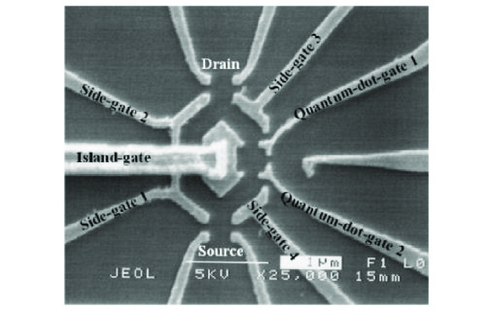
Figure 1 shows a gate-defined closed-loop AB interferometer, fabricated on a wafer of GaAs/Al0.3Ga0.7As heterostructure 2DEG. The electron density of the 2DEG was about cm-2 with the mobilities higher than cm2 V-1s-1 at 4.2 K. The 2DEG layer resided 70 nm below the surface of the wafer. The interferometer was defined by an island gate, four side gates, and two quantum-dot gates as shown in the figure. The shape of this structure is similar to the one reported previously.Yacoby The electron path inside the interferometer was defined by tuning negative voltages to these gates. Unlike a closed-loop interferometer defined by the mesa formation, Liu ; Bykov ; SO1 ; SO2 ; SO3 ; SO4 the number of transverse conducting channels (sub-bands) in each (left or right) arm could be fine-tuned by the six side gates. This was a big advantage over mesa-defined AB rings, where the existence of multiple transverse sub-bands was inevitable in practice. In our study, the number of transverse sub-bands for each path was kept close to or below one to avoid any possible interference among electrons from different transverse sub-bands. The quantum dot embedded in the interferometer in Fig. 1 was not formed during measurements of beats, despite the physical presence of the gates to form it in the sample. All the measurements were made at the base temperature of 10 mK in a dilution fridge. The corresponding electron temperature estimated from measurements of the Coulomb blockade in the quantum dot electron temp was around 140 mK. The standard phase-sensitive lock-in technique was employed to improve the signal to noise ratio. The AB magnetoconductance oscillations were taken by observing the current between the two ends (the source and the drain) of the AB ring in an excitation voltage of 10 V rms. For measurements of the WL and the SdH oscillation, a four-probe configuration was employed, where a 15-nA rms current was applied between the source and the drain while monitoring the corresponding voltage difference.
II.2 Gate-voltage dependence of beats
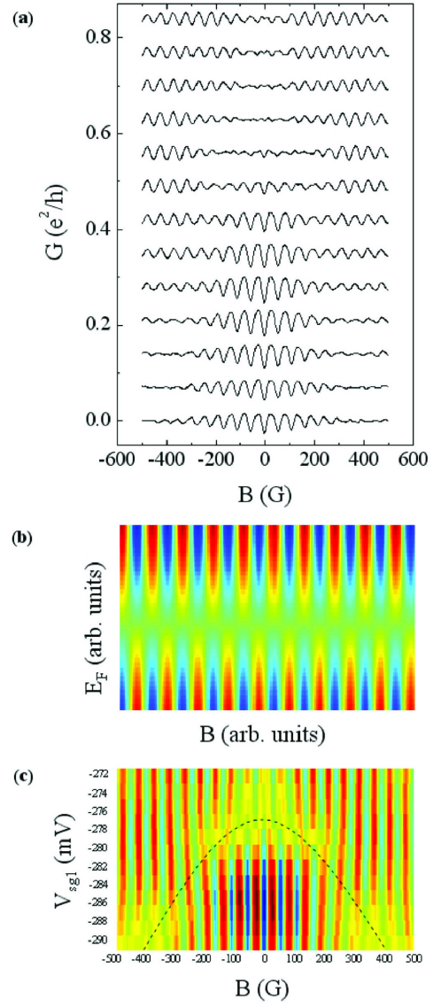
The magnetoconductance of the interferometer at various voltages of Side-gate 1 () was measured by applying a 10-V-rms excitation voltage to the interferometer, while monitoring the source-drain current. The magnetic field was swept in the range between -1500 G and 1500 G, while the was varied from -271.35 mV to -291.15 mV at intervals of 1.65 mV. Since the conductance for any was lower than it was assumed that less than an STSB STSB was open for each path of the interferometer. Since the visibility of the AB oscillation was about 2% the background current level was subtracted for clarity. As shown in Fig. 2(a) the field dependence of the conductance exhibits clear beats of AB oscillations for any values of . In addition, the phase evolved discontinuously in the variation range of . This phenomenon of the rigid phase has been observed by othersYacoby ; closed-type and interpreted by the Onsager relation in a two-terminal closed-loop interferometer.phase rigidity The relation stipulates that the electronic conductance through a closed-loop interferometer should be symmetric with respect to the =0 axis, allowing only 0 or phase. As a result, the phase change occurs only by via a double-frequency ( period) AB oscillation regime.Yacoby ; phase rigidity The expected phase change in a one-dimensional (1D) closed-loop interferometer, with an STSB per path without considering finite width of the electron path, is shown in Fig. 2(b). As in the figure, the phase stays unaltered for the variation of the Fermi energy () in the leads until it suddenly changes by . The simulation also suggests that the frequency of the AB oscillation doubles with periodicity between the transition of the two phase states. For a 1D closed-loop interferometer, with an STSB in each arm, this transition should occur at the same in all magnetic fields. In other words, as in Fig. 2(b), the transition region should be in parallel with the -field axis. In our measurements, however, the transition region distributes rather parabolically in the -vs--field plot [Fig. 2(c)]. These features were reproducible even after thermal recycling. Refs. 10 and 14 report the existence of period in the beats of AB oscillations, but without this parabolic distribution. Similar behavior was observed with the variation of the source-drain bias voltage. A parabolic distribution of the transition regions was also observed when the voltage of the island gate was varied, while fixing the voltages for all the other gates used to form the interferometer.
II.3 Strength of the spin-orbit interaction in GaAs/Al0.3Ga0.7As heterostructure
Such a beating effect without the parabolic distribution of the transition region mentioned above has been observed in various systems like metallic AB rings,Webb ; metal-ring GaAS/AlGaAs 2DEG AB rings,Liu ; Bykov GaAs/AlGaAs 2DHG rings,SO3 InAs-basedSO1 ; SO4 and InGaAs-basedSO2 2DEG rings. Although the beating features are similar to each other, interpretations of the origin of the beats are varied. Two main models suggested to explain the beats are based on picking up the Berry phase induced by the SOI and mixing of multiple conducting channels caused by the finite width of an AB ring involved. The Berry-phase-related interpretation of the beats is favored for the AB rings formed on the relatively strong SOI systems like GaAs/AlGaAs-based 2DHG, and InAs-based and InGaAs-based 2DEG’s. In contrast, the model of mixed multiple conducting channels is favored for AB rings in metallic films and GaAs/AlGaAs-based 2DEG’s with relatively small SOI.Small-SOI
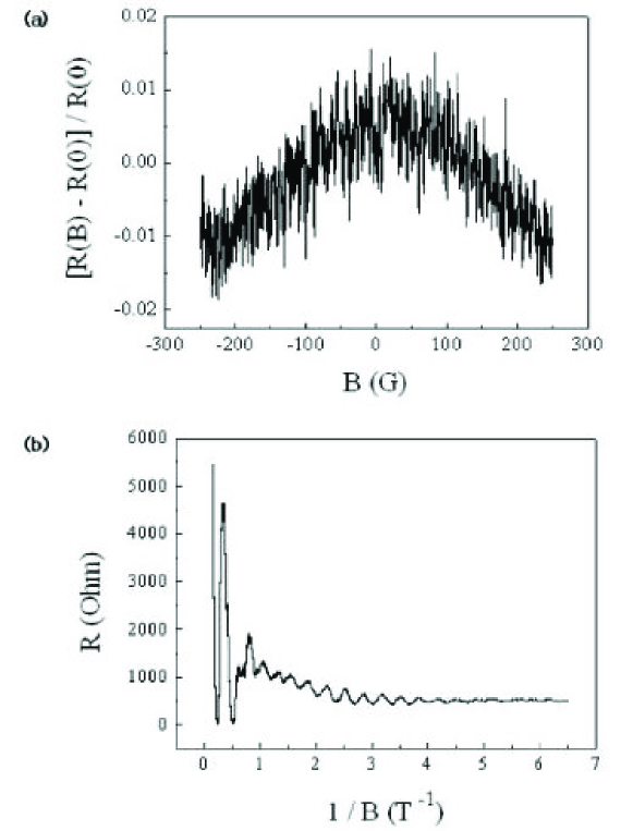
To estimate the strength of the SOI in our system, both the WL and the SdH oscillation were measured on an identical sample that was used to measure the beats. Fitting the anti-localization dip in the magnetoresistance for strong SOI materials leads to resolving the SOI strength.WL By contrast, the SOI gives two different frequencies for the SdH oscillation. It results in beats in the SdH oscillation, allowing one to estimate the SOI strength. SdH Figs. 3(a) and 3(b) illustrate the magnetoresistances of the WL and the SdH oscillation, respectively, measured in a Hall-bar geometry formed on our sample. All the gates in the interferometer were grounded during the measurements. Fig. 3(a) shows the magnetoresistance averaged over 37 measurements with the field resolution of 0.2 G, which exhibits no discernible anti-localization dips. Fig. 3(b) shows the measured SdH oscillation, without any beats, either. These results strongly imply that the SOI was very weak or almost negligible in the GaAs/Al0.3Ga0.7As heterostructure 2DEG of our interferometer. Although it is known that metallic gates may enhance the strength of the SOI, the enhancement is usually less than 30 of the original value.gatecontrol-SOI We thus expect that the SOI caused little effect on our magnetoconductance measurements.
II.4 Two-dimensional multiple-longitudinal-modes effect
In our measurements, only an STSB was set to open in each arm. The beats of AB oscillation for the STSB conduction were experimentally observed previously,Liu ; Bykov where the beats were theoretically interpreted in terms of mixing of clockwise and counterclockwise moving states of electrons with different frequencies Tan in an STSB mode. We employed the model as used in Ref. 9 to simulate the beats and the evolution of their transition region as a function of . The result indicates that the multiple longitudinal modes existing in an STSB mode generate the AB oscillations. However, the multiple longitudinal modes give more than two oscillation frequencies, with the number of the oscillation frequencies varying with the magnetic field, due to the finite width of the electron path inside the interferometer. The magnetic field dependence will be discussed in the next section in more detail.
We adopted the same form of Shrödinger equation as used in Ref. 9, but with varied parameter values to fit our experimental conditions. The eigenvalues are
| (1) |
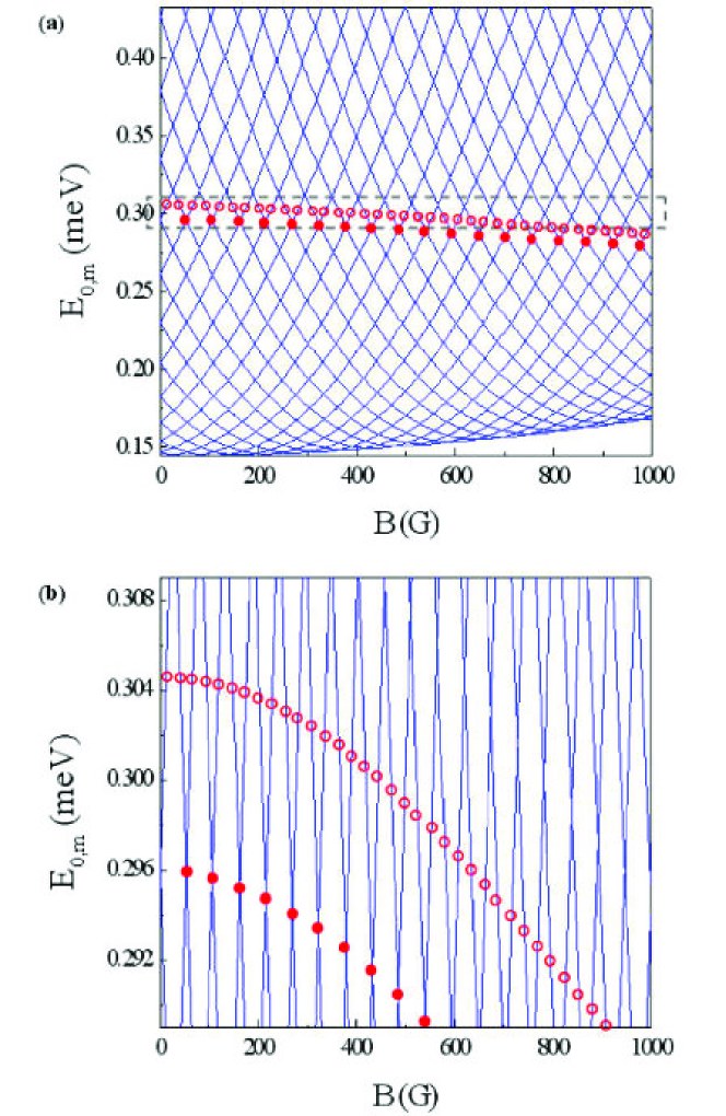
where , , , is the effective mass of the electron, is the transverse confinement strength of the gates defining the electron path, and is the average radius of the interferometer. Here, the quantum number is the transverse sub-band index and is related with the longitudinal motion.Tan In our measurements, we tuned the interferometer to have an STSB, corresponding to =0. In Fig. 4(a), the energy band is shown for an STSB mode with and 30.
As shown in Fig. 4(a), several conducting modes exist even for an STSB mode because of the existence of multiple longitudinal modes. The corresponding energy eigenvalues depend on as well as . For this dependence, the dispersion of the bands is asymmetric about the band minima. The minima shift to higher energies for nonzero magnetic fields,Tan which result in breaking of the discrete symmetry under the translation along -axis. As indicated by filled (open) circles in the figure, this makes band crossing (splitting) points respond nonlinearly to the applied magnetic field. Fig. 4(b) is an expanded band diagram of the region in the dashed box in Fig. 4(a). The band-splitting points show a clear downturn curvature as represented by open circles, the shape of which is very similar to that of the conductance with the period in Fig. 2(c).
The conductance for a given Fermi energy in the dashed-box region in Fig. 4(a) was calculated using the Landauer-Büttiker formulaLandauer-Buttiker
| (2) |
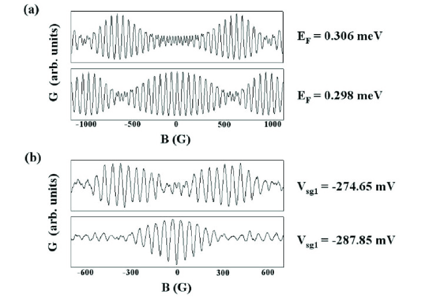
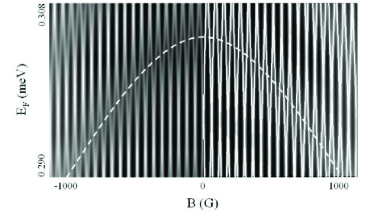
where only is taken into account and the transmission probability via an eigen mode is given by the Breit-Wigner formula at zero temperature. Here, is the coupling constant between the emitter (or the collector) and the AB ring. The was set at 3% of , which corresponds to a weak coupling regime of the system. The calculated results are shown in Fig. 5(a). The conductance shows a clear beat pattern with a variation of the envelope as a function of . Fig. 5(b) shows similar behavior observed experimentally for varied . The figures indicate that the () oscillation predominates in the nodes (antinodes) of the beats. The region of dominant oscillation appears in different magnetic fields as is varied. A grey-scale plot of the calculated conductance is shown in Fig 6. The was set to the range in the dashed square box in Fig. 4(a). The band shown in Fig. 4(b) is overlapped on the grey-scale plot by white solid lines. Contrary to the results calculated for an STSB in a 1D interferometer as in Fig. 2(b), the region where the nodes of the beats appear shows an oscillation and distributes parabolically in an -vs--field plot. This result is in qualitative agreement with our observation shown in Fig. 2(c). Clearer revelation of the double frequency region in the simulation may be from smaller value and higher visibility of AB oscillations than those in the measurement. The parabolic evolution of the node region can be naively understood with the band diagram shown in Fig. 4. According to Eq. (2) the overall conductance through an AB ring is determined mainly by the bands located close to . Hence, if is at a crossing point of two bands (marked by a filled circle in the figure) the oscillation becomes predominant. By contrast, the oscillation predominates if is at a band splitting point marked by an open circle in the figure. The conductance itself is bigger for oscillation, since two longitudinal modes simultaneously contribute to the conductance, while a single longitudinal mode contributes to the conductance for oscillation. This is the reason why () oscillation is dominant in the antinodes (nodes). Since these band crossing (splitting) points evolve parabolically as a function of and , the antinodes (nodes) also evolve in the same fashion. It should be emphasized that the finite width of the electron path in an AB interferometer is responsible for the parabolic evolution of the band crossing points. According to our simulation, however, a parabolic evolution with an upturn curvature is also possible in different regions of (not shown). Similar experimental result was also observed in a different region of the gate voltages.
The beat feature similar to Fig. 5 was reported in mesa-defined closed-loop AB interferometers,Liu ; Bykov with the results interpreted in terms of 2D multiple-longitudinal-modes effectTan in an STSB. In these works, however, no parabolic evolution of the beat pattern was reported. The parabolic evolution gives an additional confirmation of the validity of the model and better understanding of the 2D multiple-longitudinal-modes effect in an STSB. Observing the smooth evolution of the node region was possible in our study, because the number of transverse sub-bands was fine-controlled by the six individual gates, rather than by a single gate covering the whole mesa-defined AB ring as used in the other measurements. We tuned all the gates individually to leave an STSB open. Only one gate was then slightly modified to observe such an evolution.
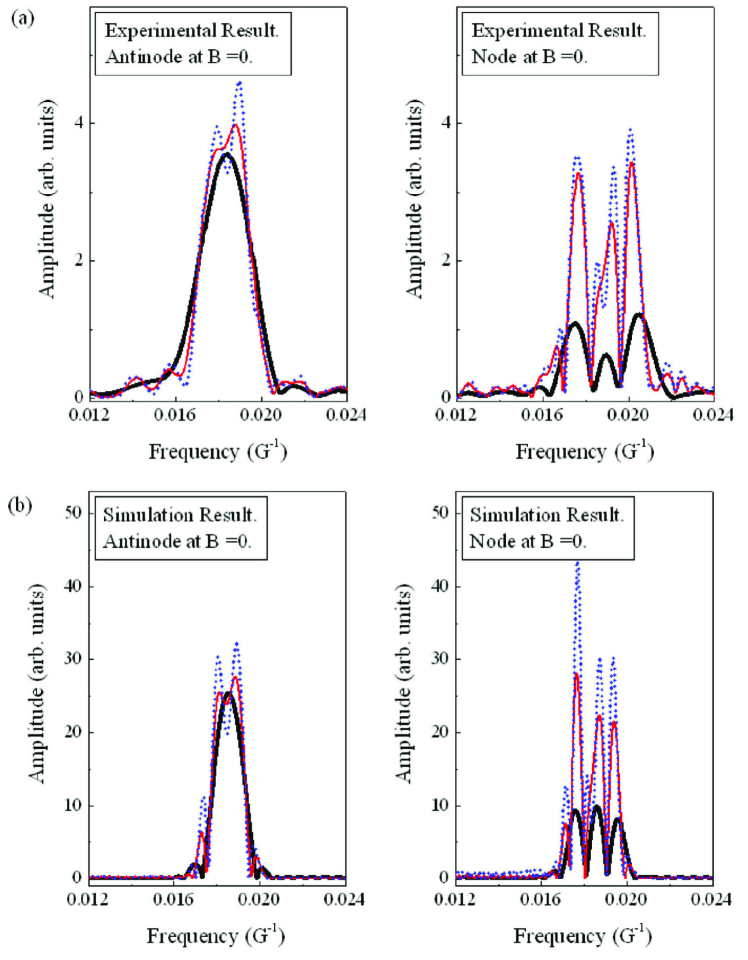
II.5 Fourier transform analysis and comparison with results from an AB ring of strong SOI
The Fourier transform analysis is a very effective way to analyze the beating of AB oscillation induced both by the multiple-conducting-channel effectLiu ; Bykov and the SOI effect.SO1 ; SO2 ; SO3 ; SO4 The Fourier spectrum gives the information on different conducting channels (or modes) inside an interferometer with very small frequency differences. In this section, we present the Fourier spectrum of two representative beats, which show the antinodes and the nodes at = 0. The zero-padding techniquezero-padding , that was used to analyze the beats induced by the SOI effect,SO3 ; SO4 was adopted for our Fourier transform analysis. The magnetoconductance data taken in the range between -1500 G and 1500 G were used for the analysis, because SdH oscillation started to appear at around 2000 G due to the high mobility of electrons in the sample. Within this range, four different widths of the Hamming windowHamming-Window (500 G, 900 G, 1200 G and 1500 G) were used. This allowed a close examination of any field-dependent effect.
The left (right) panel of Fig. 7(a) is the Fourier spectrum for the antinode (node) at =0. These two cases show different features, but their magnetic field dependencies are similar to each other. When the antinode is at =0, the Fourier spectrum shows a main center peak and a trace of small side peaks in a low magnetic field range. With increasing magnetic field, the main center peak starts to split, while the side peaks become clearer. When the node is at =0, however, the amplitudes of the main center peak and symmetric side peaks are comparable even in a low-magnetic-field range. With increasing magnetic field in this case, the center peak starts to split, while the amplitudes of the side peaks increase. Fig. 7(b) is the Fourier spectrum of the calculated magnetoconductance when an antinode and a node are at =0. The features are similar to those of the experimental Fourier spectrum.
The evolution of the Fourier spectrum as a function of the magnetic field can be naively explained as follows. First, the band crossing points marked by filled circles in the figure 4(a) give a Fourier-transform peak (the center peak). Second, open circles marked in the figure give two Fourier-transform peaks (the side peaks), where one is slightly lower and another is slightly higher than the peak given by the band crossing points. These are major three peaks shown in the spectrum. The frequency difference and the field dependence of the peaks are caused by the breaking of the discrete symmetry under the translation along the axis. Even with many energy bands around , the conductance is mainly determined by the bands close to . Thus, if the data showing an antinode at are taken for the Fourier spectrum analysis with a very narrow magnetic-field window only a center peak appears in the spectrum. As the width of the magnetic field window increases, the nodal part is included in the analysis to produce the side peaks in the spectrum. By the same analogy, if the data showing node at are taken for the analysis with a narrow magnetic field window only the side peaks appear in the spectrum. As the antinodal part is included in the analysis by enlarging the magnetic field window the center peak appears in the spectrum. These features are illustrated in Fig. 7(a). However, the experimental data given in the right panel of Fig. 7(a) show three peaks (a center peak and two side peaks) even in a low-magnetic-field range. That is because the magnetic field window is wide enough to contain the antinodes as well as the node as shown in Fig. 2(a).
Similar evolution of Fourier-spectrum peaks as a function of magnetic field was also reported in Refs. 13 and 14. Those were interpreted as evidences for the Berry phase pickup by the SOI, although the interpretation in Ref. 13 has been controversial.SO3-Reply1 ; SO3-Reply2 We believe that the evolution of peaks observed in the Fourier spectrum as a function of magnetic fields are not a conclusive evidence of the spin-orbit coupling,SO4 since the same effect is also observable in systems with negligible spin-orbit coupling. The beats in this case can be explained by the 2D effects inside the interferometer as clearly demonstrated in our study, both in experiment and in simulation. Meanwhile, the center-peak splitting and the side peaks were also observed in other magnetoconductance measurements using AB rings fabricated on strong SOI materials.SO1 ; SO2 In these works, the splitting of the center peak was focused and regarded as an evidence for the Berry-phase pickup by the SOI. It was pointed out, however, that the splitting was too large to be explained by the Berry phase pickup only. In the works, the existence of the side peaks was not clearly explained, either. As shown in our data, the splitting of the center peaks in Fig. 7(a) is around 0.001 G-1, which is comparable to those in Refs. 11 and 12. Even with almost negligible SOI in our system, the features of the Fourier spectrum of the measured magnetoconductance show a similarity to those found in strong-SOI systems.SO1 ; SO2 ; SO3 ; SO4 Our study demonstrates that the features in the Fourier spectrum can be generated irrespective of the Berry-phase pickup.
III Summary and Conclusion
The beats of AB oscillations in a closed-loop interferometer fabricated on GaAs/Al0.3Ga0.7As 2DEG were observed. Unlike mesa-defined interferometers, in our measurements, the electron path in each arm of the interferometer was kept less than a single transverse sub-band (STSB) by the fine control of six individual path-forming side gates. This enabled us to study the effect of the two-dimensional longitudinal modes developing in an STSB induced by the external magnetic field. Our simulation indicates that the experimentally observed beats of AB oscillations resulted from the multiple oscillation frequencies induced by finite width of the interferometer even with an STSB mode. The AB oscillations, imposed by the Onsager relation in our closed-loop two terminal geometry, appeared in the nodes of beats, while usual AB oscillations appeared in the antinodes, which was in agreement with our simulation results. It was also found that nodes of the beats distributed parabolically with varying the voltages of the side gates. We confirm that the phenomena can be explained by the 2D multiple-longitudinal-modes effect in the presence of an STSB, even without resorting to the strong spin-orbit interaction.
ACKNOWLEDGMENTS
This work was supported by Electron Spin Science Center in Pohang University of Science and Technology (POSTECH) and Pure Basic Research Grant R01-2006-000-11248-0 administered by KOSEF. This work was also supported by the Korea Research Foundation Grants, KRF-2005-070-C00055 and KRF-2006-312-C00543, and by POSTECH Core Research Program.
References
- (1) Y. Aharonov and D. Bohm, Phys. Rev. 115, 485 (1959).
- (2) R. A. Webb, S. Washburn, C. P. Umbach, and R. B. Laibowitz, Phys. Rev. Lett. 54, 2696 (1985).
- (3) G. Timp, A. M. Chang, J. E. Cunningham, T. Y. Chang, P. Mankiewich, R. Behringer, and R. E. Howard, Phys. Rev. Lett. 58, 2814 (1987).
- (4) A. Yacoby, M. Heiblum, D. Mahalu, and Hadas Shtrikman, Phys. Rev. Lett. 74, 4047 (1995).
- (5) A. Yacoby, R. Schuster, and M. Heiblum, Phys. Rev. B 53, 9583 (1996).
- (6) R. Schuster, E. Buks, M. Heiblum, D. Mahalu, V. Umansky, and H. Shtrikman, Nature 385, 417 (1997).
- (7) Yang Ji, M. Heiblum, D. Sprinzak, D. Mahalu, and Hadas Shtrikman, Science 290, 779 (2000); Yang Ji, M. Heiblum, and Hadas Shtrikman, Phys. Rev. Lett. 88, 076601 (2002); A.W. Holleitner, C.R. Decker, H. Qin, K. Eberl, and R. H. Blick, Phys. Rev. Lett. 87, 256802 (2001).
- (8) J. Liu, W. X. Gao, K. Ismail, K. Y. Lee, J. M. Hong, and S. Washburn, Phys. Rev. B 48, 15148 (1993).
- (9) W.-C. Tan and J. C. Inkson, Phys. Rev. B 53, 6947 (1996).
- (10) A. A. Bykov, Z. D. Kvon, and E. B. Ol’shanetskii, Proc. 22nd Int. Symp. Compound Semiconductors, pp. 909-914 (1995).
- (11) A. F. Morpurgo, J. P. Heida, T. M. Klapwijk, B. J. van Wees, and G. Borghs, Phys. Rev. Lett. 80, 1050 (1998).
- (12) F. E. Meijer, A. F. Morpurgo, T. M. Klapwijk, J. Nitta, and T. Koga, Phys. Rev. B 69, 035308 (2004).
- (13) Jeng-Bang Yau, E. P. De Poortere, and M. Shayegan, Phys. Rev. Lett. 88, 146801 (2002).
- (14) M. J. Yang, C. H. Yang, and Y. B. Lyanda-Geller, Europhys. Lett. 66, 826 (2004).
- (15) M. V. Berry, Proc. R. Soc. London, Ser. A, 392, 45 (1984).
- (16) U. Meirav, M. A. Kastner, and S. J. Wind, Phys. Rev. Lett. 65, 771 (1990).
- (17) G. Cernicchiaro, T. Martin, K. Hasselbach, D. Mailly, and A. Benoit, Phys. Rev. Lett. 79, 273 (1997); S. Pedersen, A. E. Hansen, A. Kristensen, C. B. Sørensen, and P. E. Lindelof, Phys. Rev. B 61, 5457 (2000); R. Häussler, E. Scheer, H. B. Weber, and H. v. Löhneysen, Phys. Rev. B 64, 085404 (2001).
- (18) A. D. Stone, Phys. Rev. Lett. 54, 2692 (1985); S. Washburn and R. A. Webb, Rep. Prog. Phys. 55, 1311 (1992).
- (19) P. D. Dresselhaus, C. M. A. Papavassiliou, R. G. Wheeler, and R. N. Sacks, Phys. Rev. Lett. 68, 106 (1992); C. Kurdak, A. M. Chang, A. Chin, and T. Y. Chang, Phys. Rev. B 46, 6846 (1992).
- (20) G. L. Chen, J. Han, T. T. Huang, S. Datta, and D. B. Janes, Phys. Rev. B 47, 4084 (1993); S. Pedersen, C. B. Sørensen, A. Kristensen, P. E. Lindelof, L. E. Golub, and N. S. Averkiev, Phys. Rev. B 60, 4880 (1999); T. Koga, J. Nitta, T. Akazaki, and H. Takayanagi, Phys. Rev. Lett. 89, 046801 (2002); J. B. Miller, D. M. Zumbühl, C. M. Marcus, Y. B. Lyanda-Geller, D. Goldhaber-Gordon, K. Campman, and A. C. Gossard, Phys. Rev. Lett. 90, 076807 (2003).
- (21) J. Luo, H. Munekata, F. F. Fang, and P. J. Stiles, Phys. Rev. B 38, 10142 (1988); J. Luo, H. Munekata, F. F. Fang, and P. J. Stiles, Phys. Rev. B 41, 7685 (1990); P. Ramvall, B. Kowalski, and P. Omling, Phys. Rev. B 55, 7160 (1997); W. Yang and K. Chang, Phys. Rev. B 73, 045303 (2006).
- (22) J. Nitta, T. Akazaki, H. Takayanagi, and T. Enoki, Phys. Rev. Lett. 78, 1335 (1997).
- (23) M. Büttiker, Y. Imry, R. Landauer, and S. Pinhas, Phys. Rev. B 31, 6207 (1985).
- (24) S. K. Mitra, Digital Signal Processing: A Computer-Based Approach (McGraw-Hill/Irwin, Boston, 2001).
- (25) A. V. Oppenheim, R. W. Schafer, and J. R. Buck, Discrete-time signal processing (Prentice Hall, Upper Saddle River, N.J., 1999).
- (26) Apoorva G. Wagh and Veer Chand Rakhecha, Phys. Rev. Lett. 90, 119703 (2003).
- (27) A. G. Mal’shukov and K. A. Chao, Phys. Rev. Lett. 90, 179701 (2003).
- (28) In our measurements, we first checked separately that the paths between each of six gates (side gates 1,2,3,4, and quantum-dot gates 1,2 in Fig. 1) and the island gate (in Fig. 1) gave a single transverse sub-band mode by tuning each corresponding conductance below . We then checked the conductance through the interferometer as a whole to be lower than . This confirmed us that the interferometer kept only a single transverse sub-band mode. The resulting conductance with the subtraction of the background revealed clear AB oscillations with beats even for a low visibility.
FIGURE CAPTIONS
Figure 1. SEM image of the gate-defined closed-loop Aharonov-Bohm
interferometer fabricated on a GaAs/Al0.3Ga0.7As
heterostructure two-dimensional electron-gas layer.
Figure 2. (color) (a) The magnetoconductances for various voltage
to Side-gate 1, , after subtracting the smooth
backgrounds from the raw data, as a function of magnetic fields.
The magnetic field was varied from -500 G to 500 G, while
from -271.35 mV (top) to -291.15 mV (bottom) at
intervals of 1.65 mV. (b) The phase rigidity expected in a
one-dimensional closed-loop AB-ring is illustrated. (c) The
two-dimensional pseudocolor plot of the magnetoconductance shown
in (a). A double frequency regime is guided by the dashed line.
For both pseudocolor plots, the red (blue) color represents the
high (low) magnetoconductance.
Figure 3. (a) Normalized magnetoresistance averaged over 37
independent measurements and (b) the longitudinal Hall resistance
of a Hall-bar structure, both plotted as a function of magnetic
fields.
Figure 4. (color online) (a) The calculated energy-band diagram of
a two-dimensional AB ring. The energy eigenvalues for 0 and
30 modes are plotted as a function of magnetic fields.
Multiple bands correspond to different values. The filled
circles denote the band-crossing points, while the open circles
denote the middle point between two neighboring band-crossing
points. (b) The band diagram of the dashed-box region in (a),
enlarged for clarity.
Figure 5. (a) The magnetoconductance calculated for =0.306
meV and 0.298 meV, where the Fermi energies were set to lie in the
lowest sub-band to simulate the measurement condition. (b)
Measured magnetoconductance for =-274.65 mV and -287.85
mV.
Figure 6. (color online) Grey-scale plot of the conductance,
calculated for a two-dimensional electron-gas AB-ring, as a
function of and magnetic field, where the band shown in Fig.
4(b) is overlapped in white solid lines. The white dashed line is
a guide to denote the region where the oscillation is
dominant.
Figure 7. (color online) (a) The Fourier spectrum of the
magnetoconductance measured at different in a few
magnetic-field windows. In the left (right) panel, with
=-289.50 mV (-277.95 mV), the antinode (node) of beats was at
=0. In the left (right) panel, the magnetic field was varied in
the ranges of 500 G (500 G), 900 G (1200 G),
and 1200 G (1500 G), indicated by the thick solid line,
the thin solid line, and the dotted line, respectively. (b) The
Fourier spectrum of magnetoconductance calculated for
different values of and a few magnetic-field windows are
shown for comparison. In the left (right) panel, with =0.297
meV (0.305 meV), the beating features for =0 are similar to
those of (a). In the left (right) panel, the magnetic field was
varied in the ranges of 800 G (800 G), 1200 G
(1600 G), and 1600 G (2400 G), indicated by the
thick solid line, the thin solid line, and the dotted line,
respectively.