Spin injection from Fe into Si(001): ab initio calculations and role of the Si complex band structure
Abstract
We study the possibility of spin injection from Fe into Si(001), using the Schottky barrier at the Fe/Si contact as tunneling barrier. Our calculations are based on density-functional theory for the description of the electronic structure and on a Landauer-Büttiker approach for the current. The current-carrying states correspond to the six conduction band minima of Si, which, when projected on the (001) surface Brillouin zone (SBZ), form five conductance hot spots: one at the SBZ center and four symmetric satellites. The satellites yield a current polarization of about 50%, while the SBZ center can, under very low gate voltage, yield up to almost 100%, showing a zero-gate anomaly. This extremely high polarization is traced back to the symmetry mismatch of the minority-spin Fe wavefunctions to the conduction band wavefunctions of Si at the SBZ center. The tunneling current is determined by the complex band structure of Si in the [001] direction, which shows qualitative differences compared to that of direct-gap semiconductors. Depending on the Fermi level position and Schottky barrier thickness, the complex band structure can cause the contribution of the satellites to be orders of magnitude higher or lower than the central contribution. Thus, by appropriate tuning of the interface properties, there is a possibility to cut off the satellite contribution and to reach high injection efficiency. Also, we find that a moderate strain of 0.5% along the [001] direction is sufficient to lift the degeneracy of the pockets so that only states at the zone center can carry current.
pacs:
72.25.Hg,85.75.-dI Introduction
The electrical injection of spin polarized carriers, in short called electrical spin injection, into the conduction band of semiconductors, is one of the key elements for realizing spin transistors such as the one proposed by Datta and Das.Datta90 Following arguments by Schmidt and co-workers,Schmidt00 Rashba,Rashba01 and Fert and Jaffrès,Fert01 it was realized that efficient spin injection requires the presence of a tunnel barrier at the ferromagnet/semiconductor interface. Significant experimental success started in 2001-2002,Hanbicki02 in junctions that contained a tunnel barrier between the ferromagnetic metal and the semiconductor, either in the form of the Schottky barrier of the semiconductor itself or in the form of an ultra-thin film of some other insulating material,Erve04 such as AlO or MgO.Jiang05 Most works have focussed on injection into GaAs,Hanbicki02 ; Erve04 ; Jiang05 where the current polarization can be optically detected in GaAs/AlGaAs/GaAs quantum wells. Recently, however, electrical spin injection into Si has also been demonstrated both via electrical spin detectionAppelbaum07 ; Huang07a ; Huang07b and optical detectionJonker07 with impressively large spin coherence length, reaching up to 350 m.Huang07b
The present work was motivated by the increasing experimental activity in the direction of spin injection and manipulation in Si,Appelbaum07 ; Huang07a ; Huang07b ; Jonker07 ; Min06 ; Uhrmann08 as well as by arguments for advantages of spin transport in Si.Zutic06 Based on density-functional calculations we examine the possibility of direct spin injection from Fe into Si, with the Schottky barrier of Si used as the necessary tunneling barrier. We focus on idealized epitaxial, atomically flat Fe/Si(001) interfaces. After briefly presenting the magnetic structure of the Fe/Si interface, we discuss the tunneling properties of Si based on the concept of complex band structure. We then show that spin injection is possible and can be tuned by adjusting the Fermi level in the band gap of Si in the tunneling region, or by straining Si in the injection region in order to cut off satellite contributions. We further discuss the so-called -point rule for increased injection efficiency and show that, in the case of Fe/Si, it is harder to satisfy than in Fe/GaAs.
II Method and details of calculation. Limitations of approach
The electronic structure of the junctions was calculated within the local (spin) density approximation, L(S)DA, to density functional theory. The Kohn-Sham equations were solved using the screened Korringa-Kohn-Rostoker (KKR) Green function method.tbkkr A non-relativistic treatment was chosen, as it is known that relativistic corrections result in a reduction of the calculated semiconductor gaps within the LDA. The atomic sphere approximation was used in most cases, except in particular tests which were performed with a full potential treatment. The conductance was calculated in the zero-bias limit within a Landauer-Büttiker approach adjusted to the KKR Green function method.Mavropoulos04
The self-consistent electronic structure of the junction was calculated using the decimation techniquedecimation for the consideration of the half-infinite leads. An angular momentum cutoff of was used. The details of the electronic structure that are important here change only little between and ; for example, the spin moment of bcc Fe changes by less than 5%. However, an angular momentum cutoff of was necessaryMavropoulos04 for the calculation of the conductance matrix elements.
The Fe/Si(001) interface was taken to be ideal (atomically flat). Contrary to the wavefunctions, the perturbation of the potentials dies out relatively fast with the distance from the interface. Within a finite region of two atomic layers around the interface, the potentials are perturbed from their bulk-like values and calculated self-consistently by sandwiching 5 layers of Si between two Fe leads. This way also provides the band alignment between Fe and Si. Subsequently the half-infinite Si lead is constructed by maintaining the potentials only up to the middle of the junction (left Fe lead and Si up to third layer), and repeating the potential of the third Si layer (which is considered already bulk-like) ad infinitum by use of the decimation technique. The decimation technique is also used to produce the half-infinite, bulk-like Fe lead. The same method has been applied in previous works on Fe/GaAs and Fe/ZnSe.Wunnicke02 ; Wunnicke04 .
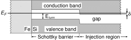
We consider the following external parameters that are involved in an injection experiment (see also Fig. 1). Firstly, the Schottky barrier has a thickness of layers and a height determined by the band alignment of Si with respect to the Fermi level of Fe. Experimentally, this can be adjusted by appropriate doping or by a gate voltage. In the calculations, this is simulated by adding an appropriate constant shift to the Si potentials up to , so that, within the barrier, the bands are shifted and (which is fixed by the Fe lead) falls at a desired position between the valence band and conduction band edges, and : . In this step the first two Si layers at the interface are excluded, as it is considered that their electronic structure will be mainly affected by their proximity to Fe. Secondly, after the barrier region the band alignment must be such that the injected electrons arrive in the Si valence band. Experimentally the appropriate band alignment can also be adjusted by a gate voltage or by doping. Here, it is again accounted for by adding a proper energy constant to the potentials of all Si layers from and on, so that falls slightly in above : . In the present work meV (2 mRyd) was used except where otherwise indicated.
A few comments are in order on the chosen band diagram. Firstly, in experiment a Schottky barrier will possibly have a different, less abrupt shape. We defer this question for Sec. VI, because after the discussion has revealed the effect of the positioning of in the gap. Secondly, the chosen value of meV can be perhaps reasonable for GaAs, but would probably result in an unrealistically high carrier concentration in Si due to the high Si effective mass. This choice helps in visualizing and understanding the current distribution in the SBZ. In Sec. V we also show calculations with up to 1.4 meV, which in fact reveal a qualitative change of injection efficiency.
It is well known that local density-functional theory (as is the LDA or the generalized gradient approximation) underestimates the gap in semiconductors and insulators; in the present calculations the Si band gap is found to be approximately 0.38 eV. Thus, the values of tunneling conductance obtained within density-functional calculations can only provide qualitative understanding, including trends, but not quantitatively correct results. Qualitatively, the underestimated band gap in the tunneling region can be partly compensated by increasing the barrier thickness . Here, was varied up to 60 Si layers.
Especially for the calculation of the bulk Si band structure (including the complex band structure), significant quantitative improvement can be achieved by using an orthogonalized plane wave method with pseudopotentials fitted to optical excitation experiments. Here we followed such a method with the parameters taken from Ref. [Cohen66, ]; in the presentation of the results we indicate when this method has been used.
Furthermore we note that an atomically flat interface is, at this point, an idealization. In an experiment, most likely interface roughness and some form of iron silicide will be present at the interface. However, it cannot be excluded that good quality, atomically almost flat interfaces can, in principle, be made, as has been achieved in Fe/MgO junctions. Moreover, the parameter space becomes simply too big if many possibilities of interface structure are to be calculated. Since modern experimental techniques allow for a detailed imaging of the interface structure,Zega06 it is possible to relate further calculations to such experimental input. In Sec. VI we point out which calculated properties are specific to the idealization of a flat interface.
Finally we comment on the lattice mismatch of Fe and Si. The Si lattice constant (5.43 Å) is approximately twice the one of Fe (2.87 Å) with a mismatch of about 5%. We adopt the Si lattice constant for the calculation (the in-plane unit cell accommodates now two Fe atoms per Fe layer), to simulate the situation where a thin film of Fe is in contact with a thick Si barrier. The stress on the Fe contacts will be appreciable, but it is sufficient that Fe retains the prescribed epitaxial structure for only a few layers for the our conclusions to be correct. This has been demonstrated in calculations on Fe/MgO/Fe junctions,Heiliger07 where it was shown that the transport properties depend on the structure of the Fe lead only close to the interface: even if Fe becomes amorphous a few layers away from the interface, the spin filtering properties practically do not change. However, the choice of lattice constant does affect the moments significantly, and therefore tests on interface relaxation and tetragonalization were made, as we discuss in Sec. III.
III Spin moments at the interface. Effect of lattice constant
The spin moment of bulk Fe was found not to change too much with lattice constant: a moment reduction of 12% was calculated at the Si lattice constant compared to the result at the Fe lattice constant. However, the change of the moments at the interface is appreciable. At the Si lattice constant, the moments of the interface Fe atoms are reduced to approximately half their bulk value, as is shown in Fig. 2. This effect, previously reported, e.g., in Ref. [Freyss02, ], is not present in calculated junctions at the Fe lattice constant, where the interface Fe moments are not suppressed at all.
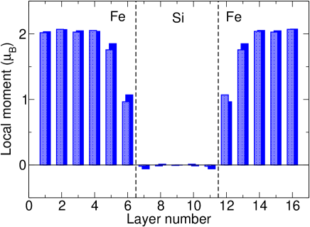
The magnetic structure was further tested by calculating a finite slab of 4 layers Fe/ 4 layers Si / 4 layers Fe with a full potential treatment and . Here the in-plane lattice constant of Si was adopted, while the Fe layers were allowed to assume an optimal ratio, and the interlayer distance at the interface was relaxed. No qualitative differences were found compared to the results using the Si lattice constant for and : the strong suppression of the moments was still present.
We conclude that a strong suppression of the Fe interface moment is unavoidable if the in-plane lattice parameter of Si(001) is adopted. Interestingly, this does not qualitatively affect the transport properties that interest us here, in particular the spin polarization of the injected current. This was found by test calculations of spin injection in a Fe/Si(001) junction using the Fe lattice parameter (whence the moments at the interface where not compromised).
IV Role of Silicon real and complex band structure
Silicon has an indirect band gap. The valence band has a maximum at the point (), while the conduction band has six equivalent degenerate minima at with ( is the lattice parameter). These properties are most important for a qualitative discussion of the tunneling conductance and electron injection.
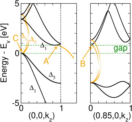
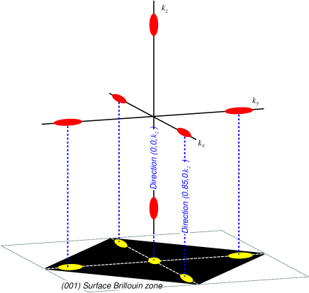
The results of this section were obtained by using pseudopotentials fitted to optical transitions.Cohen66 The band structure of Si around the gap is shown in Fig. 3. The conduction band around the minima forms six ellipsoidal “pockets” of highly anisotropic effective mass, as shown schematically in Fig. 4. Electron injection takes place into these pockets; if the junction growth is along the [001] direction, then the pockets are projected in five conductance hot spots on the two-dimensional (001) surface Brillouin zone (Fig. 4). One of these is at , while the other four are equivalent and form a satellite structure. (We denote by the projection of the Bloch -vector on the surface Brillouin zone.)
The pocket structure is highly important also for the tunneling properties. Setting the axis along the [001] epitaxy direction, the tunneling wavefunction at depends on the decay parameter as . The set of forms the so-called complex band structure; evidently, the lowest values of are responsible for the highest tunneling current. The value of depends on the proximity of to the Bloch eigenvalues of the same in the conduction or valence band, and on the curvature of with respect to (i.e., the effective mass in the direction). Thus the effective mass anisotropy of the pockets in the Si tunneling barrier has consequences that we now discuss.
Fig. 3 shows the complex (and real) band structure in the [001] () direction for two different values of : and ; the latter corresponds to one of the aforementioned “satellite” conductance hot spots. Arrows A and B indicate the pocket positions, and the effective mass anisotropy is evident. The indicated pocket in the left panel (arrow A) has its long axis along the direction. The complex band (in orange, arrow A) departing from the edge of this pocket has a small curvature (as it is along the long axis of the pocket), leading quickly to high values of for . On the other hand, the pocket indicated in the right panel (arrow B) has its long axis oriented in the direction. Here, the complex band along inherits a large curvature from the small axis of the pocket, and the value of remains relatively small for .
Consequently, when is in the gap but close to the conduction band edge, the tunneling current through the satellite positions dominates, while the tunneling current through the Brillouin zone center is small. However, if is lowered closer to the valence band edge, a different contribution from the Brillouin zone center becomes more important, marked by arrow C in Fig. 3. This comes about via the complex band of symmetry arising from the valence band maximum.
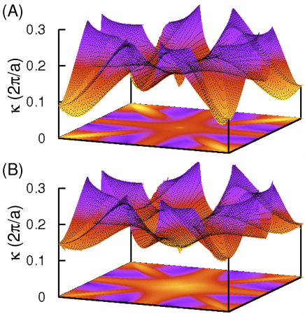
The picture becomes more complete if the full (001) surface Brillouin zone is scanned for the lowest branch of at different values of . Fig. 5 shows two such “complex Fermi surfaces”: (A) one for eV (close to ), and (B) one for eV (just a little lower than the middle of the gap). Brighter colored regions correspond to lower values of . In the first case, as is close to , the parts of the complex Fermi surface at the satellite hot spots show the lowest . As we shall see in the next section, conductance calculations also show that these regions dominate the tunneling current for an analogous choice of . In the second case shown in Fig. 5, the minimum of is found at the Brillouin zone center. Then the tunneling contribution at dominates if the Schottky barrier is thick.
We close this section with the conclusion that the indirect gap of Si lends features to the complex band structure which are qualitatively different than direct-gap compounds, as GaAs, ZnSe, or MgO. Contrary to all these direct-gap materials, where the complex band of symmetry at the Brillouin zone center gives the dominant contribution irrespective of the exact position of , in Si the positioning of can make a stark difference. This effect can have consequences for all physical properties which depend on the complex band structure. Particularly in spintronics applications it can affect spin injection, tunneling magnetoresistance, but also ground-state properties such as interlayer exchange coupling.Bruno94
V Total and spin-dependent conductance. Current polarization
We now proceed to the presentation and discussion of the ab initio results on the conductance and current polarization. We start by commenting on the effect of the underestimation of the gap in density functional theory. The conclusions of Sec. IV are qualitatively still valid, but now, within the barrier, the possible choice of is more limited (otherwise will enter the valence band). This results in an overestimation of the relative contribution of the satellites to the current. As the calculations show, the satellites dominate the current even when is at the mid-gap position; hence, calculated results at mid-gap are expected to be closer to a realistic situation of shallow tunneling close to . An overestimated proximity of to the the valence band is necessary so for the Brillouin zone center contribution to prevail. Moreover, the decay parameters and exponential falloff of the conductance with barrier thickness are underestimated.
V.1 Total conductance
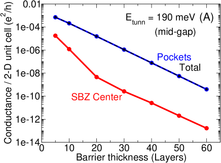
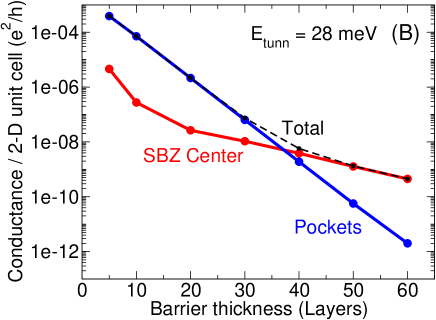
Fig. 6 shows the calculated conductance per two-dimensional interface unit cell as a function of the barrier thickness. Results for two different positions of are presented: mid-gap tunneling ( meV) and shallow tunneling close to the valence band edge ( meV). The partial contributions of the region around the Brillouin zone center and the satellites are also shown. An exponential decay with thickness is characteristic of tunneling, and the slope of the curve in a logarithmic scale is proportional to the decay parameter.
In the case of mid-gap tunneling (Fig. 6A) it is clear that the satellite contribution dominates at all thicknesses, being practically equal to the total conductance, while the central contribution to the total current is insignificant. While the slope of the satellite part of the conductance is constant, reflecting a single decay parameter , the central contribution gradually changes slope; after a thickness of about 20 layers, only the contribution remains around , with a decay parameter .
The behavior in the case of shallow tunneling, closer to the valence band edge (Fig. 6B), is analogous. Here, however, the low positioning of evidently results in (see also Fig. 3). Thus after a thickness of 35 layers the central contribution prevails and dominates the tunneling current.
In both cases we also observe that, for small thicknesses (5 layers), the satellite contribution is much stronger than the central one. Apparently there is a much stronger coupling between the Fe and Si states at the satellite positions in the Brillouin zone. At this point we have no intuitive explanation for this effect.
V.2 Spin dependent conductance and current polarization
The spin polarization of the current is defined as
| (1) |
where and are the current of majority-spin and minority-spin carriers, respectively. The difference between and arises mainly from the spin-dependent scattering at the Fe/Si interface (which gives rise to spin-dependent tunneling), due to the difference in coupling of Fe wavefunctions of different spin to Si wavefunctions at the interface.
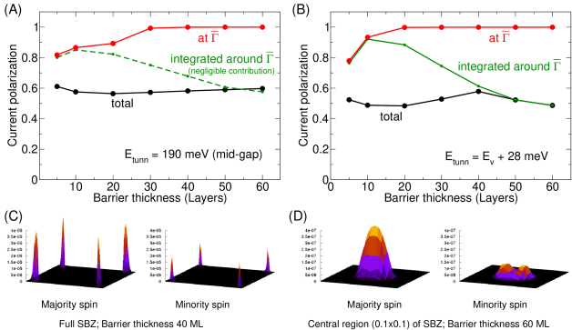
The calculated current polarization as a function of barrier thickness is shown in Fig. 7. Again, two cases are presented, corresponding to (A) mid-gap tunneling ( meV within the barrier) and (B) shallow tunneling close to the valence band edge ( meV within the barrier), as was the case in Fig. 6. These were chosen as representative of different physical situations, where the dominant contribution to the current stems from different parts of the Brillouin zone. In both cases the band alignment in the injection region (i.e., after the barrier) was chosen such that meV. Apart from the total current polarization, two contributions of special interest are shown: one at exactly the -point () and one integrated around the -point (). In terms of the -resolved current, and , these contributions are defined as
| (2) |
and
| (3) |
where the latter integration takes place in the central part of the Brillouin zone where the current is non-zero (the central hot spot of Fig. 4).
We first discuss Fig. 7A. Here the polarization is dominated by the satellite contributions for all thicknesses, as the current at the SBZ center is negligible (cf. Fig. 6A). The polarization is rather insensitive to the barrier thickness, being around . In Fig. 7C, the -resolved conductance is shown for both spin directions in the full SBZ for a barrier thickness of monolayers. Evidently the SBZ center has a negligible contribution, while the conductance at the satellite positions is higher for majority spin than for minority spin by approximately a factor of two. However, the contribution at exactly the -point shows an interesting behavior, almost reaching the ideal ; the integrated value around , , is lower. Before analyzing this we discuss Fig. 7B. Here, for small barrier thicknesses, the current is dominated by the satellites, which yield a polarization of about 50%. But for larger thicknesses, only the central contribution to the current is of significance (cf. Fig. 6B). Already at a thickness of 50 monolayers, . And again we see that, exactly at the SBZ center, .
In order to elucidate the situation at the SBZ center we show in Fig. 7D the -resolved conductance focused in the region around the point, for the case of shallow tunneling ( meV in the barrier) and a barrier thickness of 60 monolayers. The majority-spin conductance shows a single-peak structure with a maximum at the point. On the other hand, the minority-spin conductance as a function of has a double-peak structure around , with a pronounced dip at exactly which is responsible for the value .
Obviously the -point enjoys special properties. This “-point rule” has been observed and explained in previous worksWunnicke02 ; Mavropoulos02 ; Zwierzycki03 ; Wunnicke04 on spin injection from Fe into direct gap semiconductors in the zincblende structure (GaAs, ZnSe, InAs). The reason is traced back to the symmetry of the wavefunctions at , at . The semiconductor wavefunctions at have symmetry, which for Fe is present among the majority spin wavefunctions but absent among the minority spin wavefunctions at , at least in the [001] direction. This symmetry mismatch of the Fe minority spin to the semiconductor wavefunctions results in almost total reflection, so that the current is almost 100% polarized. Departing from , the Si bands acquire a mixed character, such that the Fe states (of and character), coupling to the Si complex band in the barrier, can also tunnel into the conduction band after the barrier. Then the minority-spin transmission rises, as is shown in Fig. 7D.footnote Note that no such special point appears in the satellite hot spots although their centers lie on the high-symmetry directions (along the cubic and axes).
This behavior close to is typical also for smaller thicknesses and for different tunneling energies, therefore the polarization reaches high values also in Fig. 7A. We infer that the integrated spin polarization can be increased if two requirements are fulfilled: (i) the central hot spot must be as small as possible; and (ii) the satellite contributions must be made negligible. Both can, in principle, be fulfilled, as we now discuss.
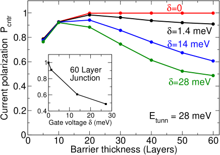
Concerning requirement (i), the radius of the hot spots depends on the injection energy in the injection region as . But is adjustable, e.g. by tuning the gate voltage of the doping concentration. In particular for Si, due to the high effective mass the value meV used in the calculations hitherto is rather high and was chosen in order to reveal the structure of the -resolved conductance, as already commented in Sec. II. By choosing a smaller , the SBZ center is approached more and more, and the integrated polarization rises. This is demonstrated in Fig. 8. At meV, is already over 90%, while in the limit we obtain . Interestingly this results in a “zero-gate anomaly” (if is considered to be a gate voltage), demonstrated in the inset of Fig. 8 where is shown as a function of at a barrier thickness of 60 layers. Evidently the polarization drops abruptly with increasing . Note that controlled injection at about meV requires low temperatures to avoid thermal broadening, since 1 meV corresponds to 11.6 K. In this respect, the -point rule is easier satisfied in direct-gap semiconductors, where due to the low effective mass the -resolved current is confined to a tiny region around also at higher .
Although Fig. 8 shows results for shallow tunneling at meV, the behavior of is entirely analogous at higher , e.g., in the case of mid-gap tunneling. Qualitatively, what changes is only the relative importance of the satellite contributions to the central contribution.
This brings us to the discussion of requirement (ii). Is it possible to cut off the satellites? We already saw that this happens as the Fermi level approaches the valence band in the barrier region, if the barrier is thick enough. But there is also another possibility, namely by tetragonally straining Si. In tetragonally strained Si the degeneracy of the six conduction pockets is lifted. In the case that , the two pockets along the axis (i.e., axis along the epitaxial direction in the presented geometry) are lowered in energy compared to the four pockets along the and axes.Buca07 Even a moderate strain of 0.5% () was calculated to lift the degeneracy by approximately 30 meV. As long as the injection energy is kept under this limit, only the central conductance hot spot will be populated in the injection region, while the satellites will be cut off.
VI Summary and concluding remarks. Outlook
Electrical injection from Fe into Si(001) through a Schottky barrier has been shown to be theoretically possible. A detailed discussion of the complex band structure of Si in the [001] direction has revealed qualitative differences in the tunneling process compared to direct-gap semiconductors. As a result of the complex band structure, the current and polarization contributions at different conduction pockets have been shown to vary very strongly depending on the Schottky barrier thickness and the position of the Fermi level in the barrier. Depending on these parameters, the injection efficiency has been found to range between 50% and 100%.
In the calculations a particular junction setup was assumed, including a number of approximations or idealizations. One approximation lies in the shape of the Schottky barrier. It was assumed that the transition from the Schottky region to the injection region is abrupt. However, but for the case of very precise interface engineering (e.g. with an appropriate doping profile), the transition to the injection region is more gradual. This would result in position-dependent decay parameters, with the central part of the SBZ providing better tunneling close to the interface (where the middle of the gap should be at ) and the satellite positions being more efficient close to the injection region (where is lowered towards ). Thus, overall, either the SBZ center or the satellites would dominate the tunneling current, depending on the exact shape of the barrier.
An idealization was that of an atomically flat Fe/Si interface, with the in-plane lattice structure unaltered. While possible in principle, in practice it can prove hard to achieve. If the two-dimensional periodicity is violated at the interface, then the most severe consequence (as regards the results presented in the present work) is expected to be the absence of excellent spin filtering at the -point. As was mentioned earlier, the extreme current polarization stems from the symmetry mismatch of the Si and minority-spin Fe wavefunctions at . Such symmetry arguments do not hold any more in the absence of perfect interface epitaxy. It has been shown,Zwierzycki03 e.g., in Fe/InAs(001) spin injection (where the same principle holds), that increasing interface disorder leads to a decrease of current polarization. However, a few perfectly epitaxial Fe layers should be enough for a symmetry-induced polarization. This has been found in an analogous case of symmetry-induced polarization in Fe/MgO/Fe(001) tunnel junctions.Heiliger07 Furthermore, it should be noted that, since an MgO barrier is known to be selective of the states at , it can also be used to increase the efficiency in spin injection experiments. Efficient spin injection has been found in FeCo/MgO/GaAs and FePt/MgO/GaAs junctions,Jiang05 while work in this direction has been reported also for FeCoB/MgO/Si junctions.Uhrmann08
A reduction of efficiency can also be caused by the formation of iron silicide at the interface, which can sometimes lead to non-collinear magnetic ordering. This can be avoided by inserting a nonmagnetic metal between Fe and Si (as was done, e.g., in Refs. Huang07a, ; Huang07b, ); calculations on such junctions will be the object of future work.
Acknowledgements
It is a pleasure to thank Prof. G. Kioseoglou and Prof. I. Appelbaum for enlightening discussions on the current state of the art in spin injection experiments in Si, and Prof. S. Blügel for his support and help throughout this project.
References
- (1) S. Datta and B. Das, Appl. Phys. Lett. 56, 665 (1990).
- (2) G. Schmidt, D. Ferrand, L.W. Molenkamp, A.T. Filip, and B.J. van Wees, Phys. Rev. B 62, R4790 (2000).
- (3) E.I. Rashba, Phys. Rev. B 62, R16267 (2000).
- (4) A. Fert and H. Jaffrès, Phys. Rev. B. 64, 184420 (2001).
- (5) A.T. Hanbicki, B.T. Jonker, G. Itskos, G. Kioseoglou, and A. Petrou, Appl. Phys. Lett. 80, 1240 (2002).
- (6) O.M.J. van’t Erve, G. Kioseoglou, A.T. Hanbicki, C.H. Li, B.T. Jonker, R. Mallory, M. Yasar, and A. Petrou, Appl. Phys. Lett. 84, 4334 (2002).
- (7) X. Jiang, R. Wang, R. M. Shelby, R. M. Macfarlane, S. R. Bank, J. S. Harris, and S. S. P. Parkin, Phys. Rev. Lett. 94, 056601 (2005); A. Sinsarp, T. Manago, F. Takano, and H. Akinaga, Japn. J. Appl. Phys. 46, L4 (2007).
- (8) I. Appelbaum, B. Huang, and D.J. Monsma, Nature 447, 295 (2007).
- (9) Biqin Huang, Lai Zhao, Douwe J. Monsma, and Ian Appelbaum, Appl. Phys. Lett. 91, 052501 (2007).
- (10) Biqin Huang, Douwe J. Monsma, and Ian Appelbaum, Phys. Rev. Lett. 99, 177209 (2007); Biqin Huang and Ian Appelbaum, Phys. Rev. B 77, 165331 (2008).
- (11) B.T. Jonker, G. Kioseoglou, A.T. Hanbicki, C.H. Li, and P.E. Thompson, Nature Physics 3, 542 (2007).
- (12) B. C. Min, J. C. Lodder, R. Jansen, and K. Motohashi, J. Appl. Phys. 99, 08S701 (2006).
- (13) T. Uhrmann, T. Dimopoulos, H. Brückl, V. K. Lazarov, A. Kohn, U. Paschen, S. Weyers, L. Bär, and M. Rührig, J. Appl. Phys. 103, 063709 (2008).
- (14) Igor Žutić, Jaroslav Fabian, and Steven C. Erwin, Phys. Rev. Lett. 97, 026602 (2006).
- (15) K. Wildberger, R. Zeller, and P. H. Dederichs, Phys. Rev. B 55, 10074 - 10080 (1997); N. Papanikolaou, R. Zeller, and P.H. Dederichs, J. Phys.: Condens. Matter 14 2799 (2002).
- (16) P. Mavropoulos, N. Papanikolaou, and P.H. Dederichs, Phys. Rev. B 69, 125104 (2004).
- (17) B. Wenzien, J. Kudrnovsky, V. Drchal and M. Sob, J. Phys.: Condens. Matter 1, 9893 (1989).
- (18) O. Wunnicke, Ph. Mavropoulos, R. Zeller, P. H. Dederichs, and D. Grundler, Phys. Rev. B 65, 241306 (R) (2002).
- (19) O. Wunnicke, Ph. Mavropoulos, R. Zeller, and P.H. Dederichs J. Phys.: Condens. Matter 16, 4643 (2004).
- (20) Marvin L. Cohen and T. K. Bergstresser, Phys. Rev. 141, 789 (1966).
- (21) Thomas J. Zega, Aubrey T. Hanbicki, Steven C. Erwin, Igor Zutic, George Kioseoglou, Connie H. Li, Berend T. Jonker, and Rhonda M. Stroud, Phys. Rev. Lett. 96, 196101 (2006).
- (22) C. Heiliger, M. Gradhand, P. Zahn, and I. Mertig Phys. Rev. Lett. 99, 066804 (2007).
- (23) M. Freyss, N. Papanikolaou, V. Bellini, R. Zeller, and P. H. Dederichs, Phys. Rev. B 66, 014445 (2002).
- (24) Interlayer exchange coupling of ferromagnetic layers separated by an insulator depends on the insulator complex band structure. See, e.g., P. Bruno, Phys. Rev. B 49, 13231 (1994).
- (25) Ph. Mavropoulos, O. Wunnicke, and P.H. Dederichs Phys. Rev. B 66, 024416 (2002).
- (26) M. Zwierzycki, K. Xia, P. J. Kelly, G. E. W. Bauer, and I. Turek Phys. Rev. B 67, 092401 (2003).
- (27) As was discussed previous papers on Fe/GaAs and Fe/ZnSe,Wunnicke02 ; Mavropoulos02 ; Wunnicke04 the polarization at may be less than 100%, because the point group rotational symmetry around the [001] axis is for Fe but for the zincblende or diamond structure. Thus, minority-spin Fe states of symmetry ( character) at can weakly couple to semiconductor states of symmetry. This weak coupling was foundWunnicke04 to result in resonant interface states penetrating the Schottky barrier, which under certain conditions reduced by 10-20%. Such a strong contribution from interface states is not observed in Fe/Si(001).
- (28) Such strain is experimentally feasible, and has the additional advantage of achieving improved mobility. See, e.g., D. Buca, B. Hollander, S. Feste, St. Lenk, H. Trinkaus, S. Mantl, R. Loo, and M. Caymax, Appl. Phys. Lett. 90, 032108 (2007).