Subwavelength Diffraction Management
Matteo Conforti, Massimiliano Guasoni, and Costantino De Angelis
Consorzio Nazionale Interuniversitario per le Scienze Fisiche della Materia, Dipartimento di Elettronica per l’Automazione, Università di Brescia, via Branze 38, 25123 Brescia, Italy
Abstract
We study light propagation in nanoscale periodic structures composed of dielectric and metal in the visible range. We demonstrate that diffraction can be tailored both in magnitude and in sign by varying the geometric features of the waveguides. Diffraction management on a subwavelength scale is demonstrated by numerical solution of Maxwell equations in frequency domain.
OCIS codes: 050.6624, 250.5403, 130.2790, 160.3900
The miniaturization of photonic devices for confining and guiding electromagnetic energy down to nanometer scale is one of the biggest challenges for the information technology industries[1]. In the last years, photonic crystals technology allowed to gain one order of magnitude factor in the miniaturization of components such as waveguides and couplers with respect to conventional (i.e. based on total internal reflection) optics. However when the size of a conventional optical circuit is reduced to the nanoscale, the propagation of light is limited by diffraction. One way to overcome this limit is through surface plasmon polaritons [2], which are evanescent waves trapped at the interface between a medium with positive dielectric constant and one with negative dielectric constant, such as metals in the visible range. Even though this phenomenon has been known for a long time, in the last years there is a renewed interest in this field, mainly motivated by the will to merge integrated electronic circuits to photonic devices[3].
In this Letter we study the propagation of light in nanostructured metal-dielectric waveguide arrays (plasmonic arrays). As well known, an array of evanescently coupled single-mode waveguides exhibits power exchanges among the waveguides leading to discrete diffraction.[4, 5]. In plasmonic arrays we find peculiar diffractive phenomena and we show the possibility of diffraction management on a subwavelength scale.
The basic building block of a uniform waveguide array is the directional coupler; in the following, for the sake of clarity, we will consider only two dimensional cases: we have translational invariance along the axis, with being the propagation direction and the other transverse coordinate. In its simplest form, a directional coupler consists of two identical parallel waveguides in close proximity; as well known, the power exchange between the two waveguides can be described by ordinary differential equations coupling the modal field amplitude of waveguides 1 and 2:
| (1) |
where is the propagation constant of the waveguide mode and is the coupling coefficient, whose expression can be obtained in the framework of Coupled Mode Theory. Limiting our attention to the TM case (i.e the non vanishing field components are ,,) we have an expression valid both for -homogeneous and -periodic (photonic crystal) waveguides [6, 7]:
| (2) |
where is the permittivity of the directional coupler, is the permittivity of the isolated single waveguide 1 or 2, , and are the electric and magnetic field of the mode (or the Bloch mode in case of periodic waveguide) of waveguide 1 or 2, is the unit cell length for a photonic crystal structure and an arbitrary length in the case of translational invariance along .
In contrast with conventional optical devices based on total internal reflection where must be always positive, in the following we introduce two different plasmonic directional couplers having opposite sign of the coupling coefficient.
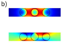
Let us first consider a system composed of alternate layers of metal (for example Silver) and dielectric (air). We describe the optical properties of the metal using a Drude free-electron model , where is the plasma frequency and is the collision frequency. As an example we consider a structure composed of 30nm of Silver and 120nm of air. We neglect absorption in metal () since it does not affect strongly the dispersive properties of the propagating modes. In Fig. 1 we show the dispersion relation and the profiles of the two modes supported by this directional coupler (to be called DC1 in the rest of the paper). In stark contrast with conventional waveguides, the fundamental mode of this structure is odd[8]. Moreover we can see that the fundamental mode has one node whereas the second one has no. This feature seems to struggle against the well known Sturm oscillation theorem[9], which states that the th order mode has exactly nodes (); however it has to be remembered that the theorem holds only if the dielectric constant is everywhere positive. Note also that the reversal of modes parity implies a negative value of the coupling coefficient[10, 11] . For example at a wavelength of 600 nm and from Eq. (2) . The difference between the two values (around 13%) is due to the strong coupling between the waveguides.
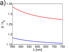
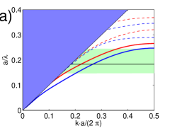
Another well known plasmonic guiding structure is the metal nanoparticle array[12], where the energy transport is supplied by electromagnetic resonant coupling between metal particles arranged in a linear chain. Double nanoparticle chains, where the electromagnetic energy is confined between two linear chains, offer a more flexible structure since the propagation is less determined by resonances[13], allowing for a larger bandwidth for the guided modes. As an example we considered double chain waveguides composed of Silver nanoparticles with a radius of 50 nm immersed in air with a longitudinal separation of 110 nm and a distance between the chains of 150 nm. We neglected losses in the metal since it was found from previous band diagram calculations of metallic photonic crystals that this is reasonable for realistic absorption coefficients [14]. In Fig. 2 we show the dispersion relation and the mode profiles of two coupled waveguides composed of three nanoparticle chains (to be called directional coupler DC2 in the rest of the paper). Since we are interested in guided modes we consider only the region in the space that lies below the light line . This coupler supports several modes, however in the working range [450nm-750nm] (light shaded region in Fig. 2a)) only two modes are reasonably below the light line. As opposed to the previous directional coupler, the fundamental mode here is even and the second order mode is odd, implying positive coupling constant. For example at 600nm we obtain and .
Let us now consider the uniform arrays A1 (A2) obtained using directional couplers DC1 (DC2) as basic building blocks. The set of equations modelling the evolution of the modal field amplitude in each waveguide of an uniform array reads as:[4, 5]
| (3) |
The diffraction coefficient[15, 16] of the waveguide array can be derived from Eqs. (3):
| (4) |
where is the spacing between the centers of adjacent waveguides and then is the imposed input field phase shift between them.
From the above reported analysis we expect, at normal incidence (), the waveguide array A1 to be an anomalous-diffraction array (), whereas waveguide array A2 is expected to behave as a normal-diffraction array (). The field evolution along the waveguide arrays has been simulated without any approximation by solving Maxwell’s equations through a frequency-domain finite-element method, using arrays composed by 17 waveguides. The central waveguide of the arrays is excited with a Gaussian field, which spreads during propagation and generates the typical diffraction pattern observed also in conventional waveguide arrays: two outermost wings and a few less intense peaks in the central waveguides. The same qualitative behavior is observed for both arrays since the intensity evolution is not influenced by the diffraction sign. On the other hand the phase front curvature of the propagating field depends on the diffraction sign. Therefore, if we alternate arrays characterized by normal and anomalous diffraction, the input field shape can be periodically recovered.
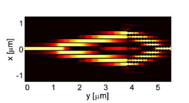
In Fig. 3 we report the finite element simulation of the diffraction-managed device. The first array section (A1) is =3900nm long, the second (A2) =1600nm. We excited only the central waveguide with a normal-incident 120nm FHWM intensity Gaussian field at 600nm. The input excitation spreads during propagation in the first section, whereas it exhibits an opposite behavior in the second one, and the initial field distribution is recovered at the output end of the device. The reported phenomena are a clear signature of the inversion of the sign of the diffraction coefficient, in perfect agreement with our theoretical analysis. It is worth noting that all the dynamics takes place in a device.
As far as losses are concerned, we verified that the propagation in the diffraction managed devices is not influenced at all by including a lossy model for the metal (Drude model gives ): the evolution showed in Fig. 3 is indistinguishable from the analogue calculated with a lossy metal. Moreover the decay length of the fundamental mode of the waveguides composing A1 is, for example, , much longer than the device length, indicating that all the relevant dynamics can take place without being suppressed by absorption.
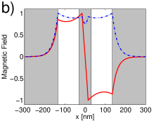
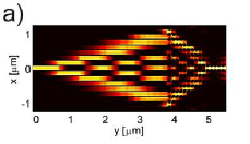
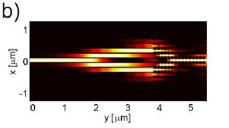
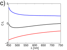
We now turn our attention to the bandwidth of the reported phenomena. By observing the band structure of the metal nanoparticle coupler (Fig. 2 a)), we expect the bandwidth of this device to be the interval [450nm,750nm], i.e all the visible range from blue to red. We studied the dynamics of diffraction management in this range and we found that, even if the two guiding structures have very different dispersive properties, the diffraction compensation is reasonably good for all the wavelengths range. Figures 4a)-b) show the time average power flow evolution at the edges of the operating frequencies interval. At short wavelengths (Fig. 4a)) the magnitude of the dielectric constant of metal is relatively low (), the fundamental mode of the waveguides is poorly confined and the coupling is strong, leading to large diffraction in both arrays. Whereas at long wavelengths (Fig. 4b)) the large magnitude of the dielectric constant of metal () leads to strong confinement and small diffraction. The average value of diffractive spreading however remains low, considering the huge band we are looking at. Figure 4 c) displays the dispersion of the diffraction parameter (coupling coefficient times propagation length ) for the arrays A1 and A2 and for the entire device.
In conclusion, diffraction properties of uniform arrays of plasmonic waveguides have been studied. Starting from the analysis of coupling between adjacent waveguides we have demonstrated that diffraction can be controlled both in amplitude and sign with normal incidence input excitations. Diffraction management in an ultracompact device composed of alternated sections with opposite diffraction sign has been demonstrated on a wavelength interval covering the visible range from blue to red.
References
- [1] S. A. Maier, Plasmonics: Fundamentals and Applications, Spinger (2007).
- [2] E. N. Economu, Surface Plasmons in thin films, Phys. Rev. 182, 539 (1969).
- [3] E. Ozbay, Plasmonics: Merging photonics and electronics at nanoscale dimensions, Science 311, 189 (2006).
- [4] D.N. Christodoulides and R.I. Joseph, Discrete self-focusing in nonlinear arrays of coupled waveguides, Opt. Lett. 13, 794 (1988).
- [5] H.S. Eisenberg, Y. Silberberg, R. Morandotti, A.R. Boyd, and J.S. Aitchison, Discrete spatial optical solitons in waveguide arrays, Phys. Rev. Lett. 81, 3383 (1998).
- [6] A. Hardy, and W. Streifer, Coupled Mode Theory of Parallel waveguides, J. Lightwave Tech., LT–3, 1135 (1985).
- [7] D. Michaelis, U. Peschel, C. Wächter, and A. Bräuer, Reciprocity theorem and perturbation theory for photonic crystal waveguides, Phys. Rev. 68, 065601(R) (2003).
- [8] X. Fan, G. P. Wang, J. C. W. Lee, and C. T. Chan, All-angle broadband negative refraction of metal waveguide arrays in the visible range: theoretical analysis and numerical demonstration, Phys. Rev. Lett. 97, 073001 (2006).
- [9] A. Zettl, Sturm Liouville theory, American Mathematical Society (2005).
- [10] C. M. de Sterke, L. C. Botten, A. A. Asatryan, T. P. White, and R. C. McPhedran, Modes of coupled photonic crystal waveguides, Opt. Lett. 29, 1384 (2004).
- [11] A. Locatelli, M. Conforti, D. Modotto, and C. De Angelis, Diffraction engineering in arrays of photonic crysral waveguides, Opt. Lett. 03, 2894 (2005).
- [12] M. Quinten, A. Leitner, J. R. Krenn, and F. R. Aussenegg, Electromagnetic energy transport via linear chains of silver nanoparticles, Opt. Lett. 23, 1331 (1998).
- [13] H. Chu, W. Ewe, E. Li, and R. Vahldieck, Analysis of sub-wavelength light propagation through long double-chain nanowires with funnel feeding, Opt. Express 15, 4216 (2007).
- [14] P. B. Catrysse, G. Veronis, H. Shin, J. Shen, and S. Fan, Guided modes supported by plasmonic films with a periodic arrangement of subwavelength slits , Appl. Phys. Lett. 88, 031101 (2006).
- [15] H.S. Eisenberg, Y. Silberberg, R. Morandotti, and J.S. Aitchison, Diffraction management, Phys. Rev. Lett. 85, 1863 (2000).
- [16] T. Pertsch, T. Zentgraf, U. Peschel, A. Bräuer, and F. Lederer, Anomalous refraction and diffraction in discrete optical system, Phys. Rev. Lett. 88, 093901 (2002).