A Sensor with Analog and Digital Pixels
in 0.15 m SOI Technology
Abstract
A monolithic pixel sensor in deep-submicron Silicon-On-Insulator (SOI) CMOS technology has been designed, manufactured and characterised. This technology is of significant interest for applications in particle tracking and imaging. The prototype chip features pixels of 10 m pitch arrayed in two analog sections and one digital section with a comparator and a latch integrated in each pixel. The prototype response has been tested with infrared lasers and with the 1.35 GeV electron beam extracted from the injection booster at the LBNL Advanced Light Source. Results from irradiation tests with low energy protons and neutrons performed at the LBNL 88-inch Cyclotron are also presented.
I Introduction
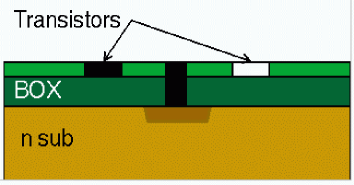
Silicon on insulator (SOI) technology allows to fabricate CMOS circuits on a thin Si layer, electrically insulated from the rest of the wafer. The isolation of the electronics from the detector volume offers clear advantages for designing pixel sensors for particle detection, compared to bulk CMOS active pixel sensors, realised in standard CMOS process. Both nMOS and pMOS transistors can be built, without disturbing the charge collection, and the detector wafer can be reversely biased, thus improving the efficiency of charge carriers collection. There have been earlier attempts to develop SOI pixel sensors for charged particle detection with a high resistivity bottom wafer. A proof of principle of the concept was obtained using a 3 m process at IET, Poland [1, 2, 3]. The availability of the 0.15 m FD-SOI process by OKI Electric Industry Co. Ltd. Japan, in cooperation with KEK, Japan, has opened up new possibilities for SOI pixel sensors with a pixel pitch, which is small enough to satisfy the requirements for the next generation of particle physics collider experiments, as well as for imaging. As shown in Figure 2, the OKI SOI process consists of an -type detector wafer, with - and -type implants. Transistors are di-electrically isolated from each other, and separated from the substrate by a buried oxide layer (BOX). The silicon film on which the transistors are grown is sufficiently thin (40 nm) and lightly doped so that it can be fully depleted at typical operating voltages. A chip based on this process has already been designed at KEK, Japan and successfully tested with an IR laser beam [4, 5].
We designed and submitted a monolithic pixel sensor chip, with 1010 m2 pixels, for charged particle detection. The chip has both analog and digital pixel cells. This paper presents the chip design and the results of its characterisation, obtained with laser beams in the lab and with the 1.35 GeV electrons beam from the LBNL Advanced Light Source (ALS) booster at LBNL.
II Prototype chip design
The chip consists of a 350 m thick high-resistivity -type substrate, with the CMOS circuitry implanted on a 40 nm thin Si layer on top of a 200 nm thick buried oxide (see Figure 2).
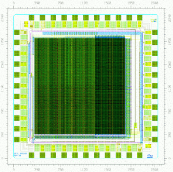
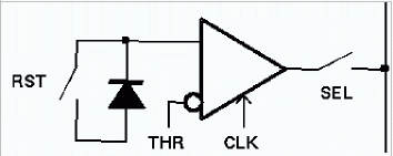
The chip features an array of 160150 pixels on a 10 m pitch. The OKI SOI technology includes thin-oxide 1.0 V transistors and thick-oxide 1.8 V transistors. The left-most 50 columns are simple analog pixels with 1.8 V transistors in a 3T-like (complementary switches) architecture. The central 50 columns implement 1.0 V analog pixels, and the right-most 50 columns are clocked, digital pixels. The digital pixel is based on a clocked comparator. When the pixel is reset, the same reset being used for the comparator, charge is accumulated on the diode capacitance. As the row is selected for readout, the comparator is clocked, and the pixel is considered to be hit if the voltage on the diode is greater than a common threshold (see Figure 3). In order to avoid static power dissipation, no amplifier is present in the digital pixels,
The 1.0 V pixels have been found to have significantly higher leakage currents than the 1.8 V pixels, which adversely affect their signal-to-noise (S/N) ratio. Each sector is divided in two subsections with 11 m2 and 44 m2 charge collecting diodes. Each 8000-pixel analog section is read out independently using a 14-bit ADC. A Xilinx FPGA controls all pixel clocks and resets. The pixels are clocked at 6.25 MHz corresponding to an integration time of 1.382 ms. Correlated Double Sampling (CDS) is performed by acquiring two frames of data with no pixel reset between the readings and subtracting the first frame from the second.
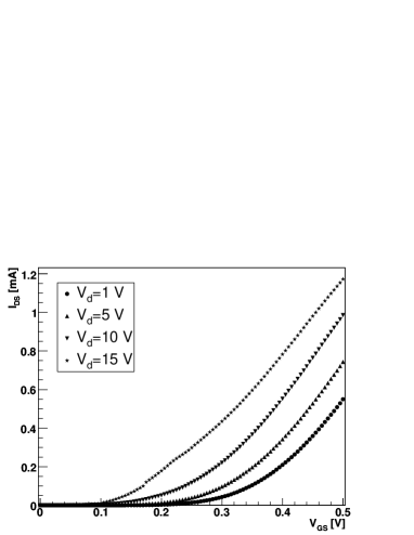
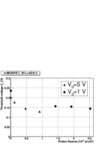
A potential limitation of the SOI technology comes from the transistor back-gating effect. The reverse bias, , applied to the silicon substrate increases the potential at the surface, so that the buried oxide acts as a second gate for the CMOS circuitry on top, typically causing a shift in the transistor thresholds for increasing depletion voltages. The effect was evaluated on single transistor test structures implemented at the chip periphery. These include complementary -type and -type MOSFETs, all with = 50 m and = 0.3 m, with different types of body contacts (floating, source-tied and gate-tied). Figure 4 shows the characteristics measured on one -type test MOSFET for substrate voltages, , up to 15 V. The transistor threshold voltage, extracted from the characteristics, shifts from = 0.24 V at = 1 V to = 0.07 V at = 15 V, consistent with an increased back-gating effect. A similar effect is also measured on -type test MOSFETs.
The back-gating effect in the chip active area is investigated using TCAD simulations implemented with the Synopsys Taurus Device package. A 2-dimensional model of a 5 pixel array is used, including a realistic geometry of the substrate contact region at the chip edges. The -type substrate is modelled with a constant doping level of 61012 cm-3, while the pixel diodes are modelled with shallow (500 nm deep) -type implants with a peak doping concentration of 11020 cm-3 at the Si surface, decreasing along a Gaussian profile towards the Si substrate.
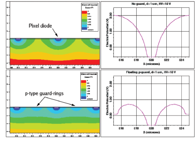
The characteristics of single transistor at the chip periphery have been simulated as a function of the substrate bias. Figure 5 compares the simulated thresholds for a n-MOSFET with the measurements performed on a test transistor, which show a qualitative agreement, within the uncertainty in reproducing the actual process parameters. The electrostatic potential at the interface between the buried oxide and the silicon substrate is simulated as a function of the substrate bias for different pixel layouts, varying the size of the charge collecting diodes and evaluating the effect of different guard-ring configurations. This study indicates that the most effective design has a floating -type guard-ring around each pixel. Figure 6 shows the guard-rings effect on the field in the area between diode implants, which limits the potential back-gating. According to this results, a floating -type guard-ring has been implemented around each pixel in the active area of the test chip. A series of floating and grounded guard-rings has also been implemented around the pixel matrix and around the peripheral I/O electronics.
III Tests with infrared lasers
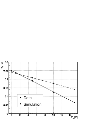
The response of the analog sections has been tested with a 1060 nm IR laser, for different values. The laser was focused to a 20 m spot and pulsed for 30 s between successive readings. We measured the signal pulse height in a 55 matrix, centred around the laser spot centre. The measured signal increases as , as expected from the corresponding increase of the depletion region, until 9 V, where it saturates, to decrease for 15 V (see Figure7). We interpret this effect as due to transistor back-gating, affecting the 1.0 V transistor pixels at lower values compared to the 1.8 V transistor pixels.
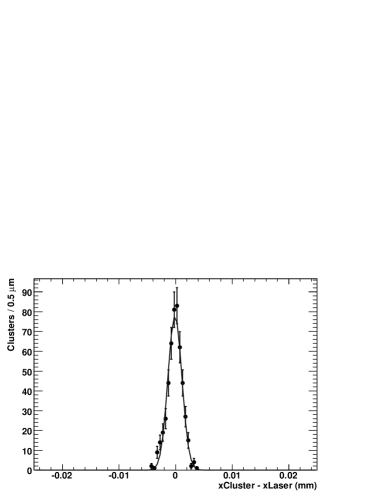
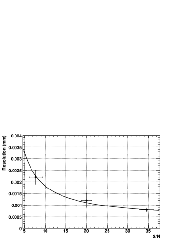
The spatial resolution of the analog pixels is determined using a 1060 nm pulsed laser beam focused to a 5 m Gaussian spot. We performed pixel scans by shifting the laser spot along single pixel rows in steps of 1 m using a stepping motor with a positioning accuracy of 0.1 m. For each position we record 500 events. We reconstruct the hit position from the centre of gravity of the reconstructed cluster charge and study the linearity between the average cluster position and the spot position, obtained from the reading of the stepping motor linear encoder. The resolution is extracted from the spread of the reconstructed cluster position for sets of events taken at each point in the scan (see Figure 8). The laser intensity is varied to obtain different S/N values, from values below that observed for 1.35 GeV electron signals up to S/N 35. Pixels with 10 m pitch have a single point resolution of 1 m for a S/N ratio of 20 or larger and the measured resolution scales as the inverse of S/N, as expected (see Figure 9). Similar results are observed also for = 10 V.
IV Tests with high-energy particle beams
| Nb Pixels | |||
|---|---|---|---|
| (V) | beam on | beam off | in Cluster |
| 20 | 3.62 | 0.02 | 1.78 |
| 25 | 5.81 | 0.03 | 1.32 |
| 30 | 8.31 | 0.03 | 1.26 |
| 35 | 1.60 | 0.02 | 1.14 |
The pixel chip has been tested on the 1.35 GeV electron beam-line at LBNL Advanced Light Source (ALS). The readout sequence of a reference frame followed by the signal frame is synchronised with the 1 Hz booster extraction cycle so that the beam spill hits the detector just before the second frame is read out. The temperature is kept constant during operation at 23∘C by forced airflow. Data are processed on-line by a LabView-based program, which performs correlated double sampling, pedestal subtraction and noise computation. The data are converted in the lcio format and the offline analysis is performed using a set of dedicated processors developed in the Marlin framework [6]. Each event is scanned for seed pixels with pulse height above a signal-to-noise threshold of 4.5. Noisy pixels are flagged and masked. Seeds are sorted according to their pulse heights and the neighbouring pixels in a 55 matrix with S/N2.5 are added to the cluster. Clusters are not allowed to overlap and we require that pixels associated to a cluster are not interleaved by any pixels below the neighbour threshold.
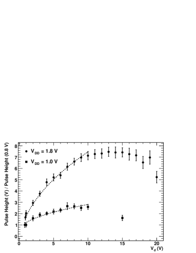
All the sections are functional. Results for two of the analog sections, with = 1.0 V and 1.8 V transistors respectively, each consisting of a 0.40.8 mm2 active region, have already been presented [7]. Data have been taken at different depletion voltages, , from 1 V up to 15 V for the analog sections, and up to 30 V for the digital section. The depletion voltages used correspond to an estimated depletion thickness of 8 m to 80 m for = 1 V to 30 V. Only a small background is found, arising from noisy pixels which survive the bad pixel cut and the cluster quality criteria adopted in the data analysis. The pixel multiplicity in a cluster decreases with increasing depletion voltage, while the cluster pulse height increases for up to 10 V. At 15 V the cluster signal and the efficiency of the chip decreases, similarly to the trend observed in the laser test. A good signal-to-noise ratio up to 15 as measured with the analog section with 1.8 V transistors for 5 V15 V.
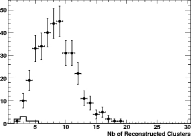
The digital section of the chip is also found to be functional. Beam signals are observed by applying depletion voltages in excess of 20 V, and up to 30 V. This can be explained by considering that the analog threshold of the in-pixel comparators is also affected by back-gating, but the digital circuitry in each pixel is only active when triggered, i.e. for times much shorter compared to that of the analog pixels. As larger substrate voltages are needed to obtain signals large enough to be above threshold, the two effects combine giving the best particle detection capabilities for 20 V 30 V. Figure 10 shows the hit multiplicity observed in the digital pixels for events taken with and without beam, for = 30 V. A clear excess of hits can be seen in the presence of beam. The average number of pixels in a cluster decreases from 1.8 to 1.3 for increasing from 20 V to 30 V (see Table I).
V Radiation hardness tests
Irradiation tests have been performed at the BASE Facility of the LBNL 88-inch Cyclotron [8]. A first test has been performed with 30 MeV protons on single transistors. The chip is mounted on the beam line, behind a 1-inch diameter collimator, and the terminals of two test transistors (one -MOSFET and one -MOSFET) are connected to a semiconductor parameter analyser so that the transistor characteristics could be measured in-between irradiation steps. During the irradiation steps, the transistor terminals are kept grounded. The irradiation was performed with a flux of 6107 p/cm2s, up to a total fluence of 2.51012 p/cm2, corresponding to a total dose of 600 kRad. Figure 11 shows the variation in the threshold voltage for the nMOS test transistor as a function of the proton fluence. An initial substrate voltage = 5 V was used, but after a fluence of about 11012 p/cm2 the transistor characteristics could not be properly measured, and a reduced substrate bias of = 1 V needed to be apply in order to recover the transistor characteristics. We interpret this effect as due to radiation-induced charge build-up in the buried oxide which effectively increases back-gating. The total threshold variation is indeed significant ( 100 mV) also for a low substrate bias (i.e. = 1 V). The effect is much larger than what would be expected at such doses from radiation damage in the transistor thin gate oxide. Similar results are obtained for the pMOSFET characteristics.
A second test has been performed on a fully functional chip exposed to a beam of 1-20 MeV neutrons, up to a total fluence of 11011 n/cm2. No change in the noise of the analog sections is observable, and no significant variation in the test transistor characteristics is detected.
VI Second prototype chip design
A second prototype chip has been designed and submitted for fabrication in the 0.20 m SOI process from OKI. This process has been is optimised for low leakage current. The chip is a 55 mm2 prototype with an active area of 3.53.5 mm2 in which 168172 pixels are arrayed with a 20 m pitch. The pixel matrix is subdivided into a 40172 pixel section with a simple, analog 3-transistor architecture, mostly intended for technology evaluation, and a 128172 pixel main section with a second-generation digital pixel cell. Each pixel has two capacitors for in-pixel CDS, and a digital latch is triggered by a clocked comparator with a current threshold. The chip design is optimised for readout up to a 50 MHz clock frequency, and the digital section has multiple parallel outputs to further improve the frame rate.
VII Summary and conclusion
A pixel chip including both analog and digital pixel cells has been designed and produced in OKI 0.15 m SOI technology. The response of the chip has been studied using both focused laser beams and the 1.35 GeV beam at the LBNL ALS. Both the analog and digital pixels are functional. In particular, on the analog pixels, a single point resolution of 1 m is estimated from a focused laser scan. The results of total ionising dose tests performed on single transistors hint at the observation of trapped charge build-up in the buried oxide, which enhances the CMOS electronics back-gate effect. No sensitivity to non-ionising dose has been observed up to a fluence of 1011 n/cm2. These results are very encouraging for the further development of monolithic pixel sensors in SOI technology. The SOI technology is of great interest for its potential to implement complex readout architectures combined with a high-resistivity, depleted substrate. Ensuring faster charge collection and larger signals SOI pixel sensors are an attractive option for application in particle tracking at future colliders as well as non-destructive beam monitoring and fast imaging of low energy radiation.
Acknowledgements
This work was supported by the Director, Office of Science, of the U.S. Department of Energy under Contract No.DE-AC02-05CH11231. We are indebted to the ALS staff for their assistance and the excellent performance of the machine.
References
- [1] J. Marczewski et al., Nucl. Instrum. Meth. A 549, 112 (2005).
- [2] J. Marczewski et al., Nucl. Instrum. Meth. A 560, 26 (2006).
- [3] H. Niemiec et al., Nucl. Instrum. Meth. A 568, 153 (2006).
- [4] Y. Ikegami et al., Nucl. Instrum. Meth. A 579, 706 (2007).
- [5] T. Tsuboyama et al., Nucl. Instrum. Meth. A 582, 861 (2007).
- [6] F. Gaede, Nucl. Instrum. Meth. A 559, 177 (2006).
- [7] M. Battaglia et al., Nucl. Instrum. Meth. A 583, 526 (2007) [arXiv:0709.4218 [physics.ins-det]].
- [8] M. A. McMahan, Proceedings of the Space Nuclear Conference 2005, San Diego, CA, June 5-9, 2005, Paper 1011.