Experimental Verification of the Quantized Conductance of Photonic Crystal Waveguides
Abstract
We report experiments that demonstrate the quantization of the conductance of photonic crystal waveguides. To obtain a diffusive wave, we have added all the transmitted channels for all the incident angles. The conductance steps have equal height and a width of one half the wavelength used. Detailed numerical results agree very well with the novel experimental results.
pacs:
Valid PACS appear hereQuantization of different physical quantities is one of the interesting phenomena in science. The quantization occurs because of the wave nature of particles. One quantity that gives strong quantization is the electrical conductance , the inverse of the resistance. It is very difficult to calculate the transport properties of small devices analytically. Landauer was the first one to make the connection between the conductance and the transmission coefficient Lan . He showed that , where is the transmission coefficient. If one has a perfect metal , then and therefore , as expected for a perfect metal. In 1981, Soukoulis and Economou souk proved, by using the Kubo-Greenwood formula, that for 1D systems . There was a fierce controversy in 1980’s regarding which formula was correct cont , since the Economou-Soukoulis formula gives a finite value for the resistance for the perfect metal. The experiments e1 ; e2 resolved this issue and indeed it was found that . Extensions to higher dimension hd1 ; hd2 were achieved for G and it was shown that for a multichannel wire the dimensionless conductance
| (1) |
where is the transmission coefficient between incident mode and output mode . The same set of modes are used for the incident and output modes. For classical waves the total is equivalent to the dimensionless conductance prl-1997 in electronic systems . For the ideal waveguide configuration, gives the number of propagation modes inside the waveguide.
The key idea of Landauer was to relate the resistance of the sample with its transmission. So the idea of quantization of conductance can be also obeyed by all types of waves, electromagnetic waves, acoustic and elastic waves. It is amazing that the only experiment exp that has been done with waves is the transmission of a slit of variable width for a given wavelength of . Similar to its electronic counterpart, the optical conductance of a structure is described as the total light transmitted through the structure from a diffusive illumination (an isotropic incoherent incident wave). So the conductance for classical waves is dimensionless. In the experiment of Montie et al. exp a two dimensional (2D) diffuser was used to achieve the diffusive illumination. The diffuser was essentially a 2D random array of scatterers through which the normally incident plane wave scatters diffusively and isotropically. The diffused light passed through a metal slit and the transmitted light was collected. The result showed that the optical conductance increases in a staircase fashion. A new step occurs when the slit width () i.e., a new mode is enabled in the slit.
Photonic crystals (PCs) can be designed to have a bandgap that prohibits wave propagation in a certain frequency range PC-book . Line defects of PCs can confine light with frequencies within the bandgap inside the channel and act as waveguides. PC waveguides have been studied extensively and many applications have been proposed PC-book . However, the concept of optical conductance was not applied to PC waveguides until recently apl-2007 ; physicaB and no experimental work has been reported to our knowledge. In this letter we study the optical conductance of photonic crystal (PC) waveguides, both numerically and experimentally. We will demonstrate experimentally that the optical conductance of a 2D PC waveguide in microwaves has the similar staircase effect as the metal slit.
We design the working frequency of the waveguide at microwave region, which makes the PC easy to be fabricated. One of the main experimental difficulties is the need of diffusive waves. It is easy to be achieved at optical wavelengths by a diffuser. For microwaves, a large enough random array of scatters are needed to act as a diffuser. Since the wavelength is now of the order of , the diffuser must be really big in size and the intensity of the transmitted waves will be too weak to be used efficiently. So we apply Eq. (1) in experiments for classical waves. We measure the transmitted power for each incident plane wave with different incident angle separately and sum them up to obtain the conductance of EM waves apl-2007 .
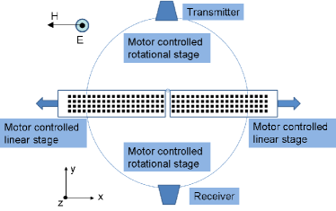
The PC we study is a 2D square array of square alumina rods. The lattice constant is mm and the square rods are of dimension mm with relative permittivity and height cm. It has a bandgap between GHz and GHz for TM modes (Electric field parallel to the rods). The waveguide is formed by two closely separated pieces of PC slabs with a size of each. The width of the waveguide () can be varied by changing the distance between the two PC slabs. HP8510B network analyzer and a pair of horn antennas are used to measure the transmission. The antennas are mounted on motorized rotational stages which can move along a circle with a radius of cm and centering at the middle of the entrance of the waveguide. So both the incident and outgoing angle can be controlled. (See Fig. 1 for details).
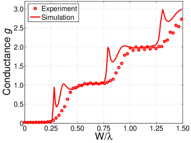
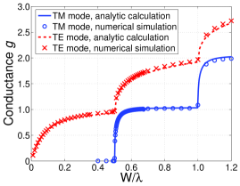
The experimental result of the optical conductance of the PC waveguide is shown together with numerical simulations in Fig. 2. We see that the optical conductance increases in a staircase manner with the increase of the waveguide width. The steps forming the staircases have essentially the same height and a new step appears at each integer multiple of . Notice that the first conductance step doesn’t start at . This is because that for the photonic crystal channel the boundaries are not well defined and the field decays exponentially inside the photonic crystal. So the waveguide is wider than .
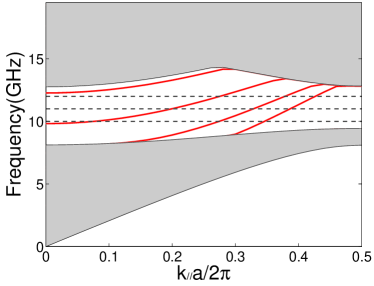
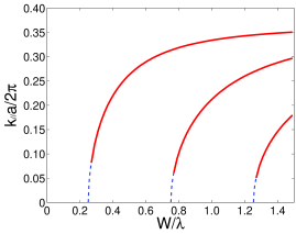
We use the commercial software COMSOL Multiphysics to do the numerical simulations. The simulation results of three frequencies are shown in Fig. 3. To understand the shape of optical conductance curves, the band structure of the PC with the channel are calculated using the supercell technique. When the channel width increases, some bands move downwards into the bandgap of the PC. Fig. 4 shows the band structure when mm. There are four impurity bands inside the band gap. The experimental frequency GHz crosses the three impurity bands. It means the channel can support three propagation modes. The propagation wave vectors of the modes can be read from the horizontal axis. Fig. 5 shows the relations between the propagation wave vectors of the propagation modes and the width of the channel when GHz based on the band structure simulations. The figure demonstrates clearly that the first propagation mode appears when and one more propagation mode when the width increase . Comparing with Fig. 3, it is clear that the optical conductance steps describes the number of propagation modes supported by the channel.
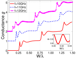
The oscillation of the optical conductance curves can also be explained by the propagation wave vectors of the channel modes. A natural explanation about the conductance oscillations is the Fabry-Pérot interference, the interference between the multiple reflection of waves inside the waveguide. The phase difference between two succeeding reflection equals the propagation phase ( is the length of the channel) plus the phase change of the reflections at the entrance and the exit of the channel. The reflection ratio changes with the channel width. To prove that the conductance oscillations are due to the Fabry-Pérot interference, we calculated the optical conductance curves for a long channel ( GHz). The inset of Fig. 3 shows the simulation result. When the channel width changes from to , the oscillation has a full period. The reflection ratio is a continuous function of the channel width. So the reflection ratio will not change too much during the period since the width doesn’t change too much. Then we neglect them and compare the propagation phases only. When , the conductance curve has a dip, a peak and another dip. The propagation phases are respectively. The phase differences between a dip and its neighboring peak are and . They agree with the Fabry-Pérot explanation.
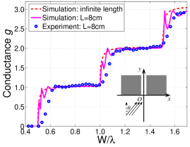
From Fig. 2 we can see that the onset of the staircases in experiments and simulations are in good agreement. However, the Fabry-Pérot oscillations are missing in the experiments. The major reason is that, while in simulations the model is perfectly 2D, we do not have an ideal 2D system in experiments. The source we get from a radiating horn antenna is a confined beam. When it encounters the PC structure, while the main part is propagating in xy plane, the beam also scatters out of the plane. Since the receiving antenna only collects the transmitted power in the xy plane where it sits, not all the transmitted power is obtained. At the onset of the staircase, more power is lost due to the multiple reflection. So the experimental curve is lower than the one obtained by simulations and the Fabry-Pérot resonances are missing.
We also studied the optical conductance of a perfect electric conductor (PEC) channel, which serves as a simplified model of the photonic crystal waveguides. Analytical calculations starting from Maxwell’s equations ana1 are performed to understand the mechanism behind the stairs.
Suppose is the interface of the air and the PEC channel. The half-space is the air and is the PEC channel. is the middle of the PEC channel (see the inset of Fig. 7).
In TM mode, the incident wave is
| (2) |
Here ; . is the wave vector in air; is the incident angle. The reflected wave is the composition of plane waves. The total electric field in the air area is
| (3) |
where , and are unknown coefficients.
The channel is infinite long; so the field in the channel is the composition of all the channel modes moving towards direction.
| (4) |
Here is the channel mode profile and .
We have defined the fields before the channel (Eq. (3)) and in the channel (Eq. (4)) separately. and should be continuous along the interface . By using these boundary conditions we can obtain the following set of equations for the unknowns :
| (5) |
Here
| (6) |
| (7) |
| (8) |
This method can be applied to TE mode too. Because of space consrains, we won’t repeat it here.
The coefficients of the channel models are solved by Equ. (5). Then the optical conductance of the infinite long channel can be calculated.
We also used COMSOL Multiphysics to simulate the infinite long channel numerically by inserting a perfect matched layer (PML) pml in the channel. The incoming channel modes are absorbed by PML without reflection. Fig. 6 shows the analytic calculation and numerical simulation results. The Fabry-Pérot oscillations disappear since the channel is infinite long. The PEC channel has at least one TE propagaion mode no matter how narrow channel is. So the first step of TE mode begins at . It is an interesting question why the conductance curves, shown in Fig. 6 , of TE and TM modes have different behavior.
Experimental measurements have also been performed and the results are shown together with the simulation results in Fig. 7 for TM mode. The experimental curve is smooth and lower than the simulation results, similar with the PC curves.
It means when the channel is wide, we can get the coefficients of the first several modes directly. Then it is easy to prove that the contribution to the optical conductance by one mode converges to 1 when the channel width goes to infinity. This is the reason for the step profile.
We have shown for the first time that the conductance of the photonic crystal waveguide is quantized in microwave frequencies. Quantization does not only occur in small length scales and in the quantum regime but also in long length scales and in the classical regime. We have also introduced new ways to obtain diffusive waves in the microwave region.
This work was partially supported by Ames Laboratory (Contract No. DE-AC0207CH11385) and EU projects Metamorphose and Phoremost.
References
- (1) R. Landauer,IBM, J. Res. Dev. 1, 223(1957); R. Landauer, Phys. Lett. A 85(2), 91 (1981).
- (2) E. N. Economou and C. M. Soukoulis, Phys. Rev. Lett. 46, 618 (1981).
- (3) For a historical account of the controversy from two different perspectives, see R. Landauer, IBM, J. Res. Dev. 32, 306 (1988) and A. D. Stone and A. Szafer, ibidem, p.384.
- (4) G. Timp et al., Phys. Rev. Lett. 59, 732 (1987).
- (5) B. J. van Wees et al., Phys. Rev. Lett. 60, 848 (1988); Phys. Rev. B 43, 12431 (1991).
- (6) D. S. Fisher and P. A. Lee, Phys. Rev. B 23, 6851 (1981).
- (7) M. Büttiker et al., Phys. Rev. B 31, 6207 (1985).
- (8) M. Stoytchev and A. Z. Genack, Phys. Rev. Lett. 79, 309 (1997).
- (9) E. A. Montie et al., Nature 350, 594 (1991).
- (10) See, for example, Photonic Crystals and Light Localization in the 21st Century, edited by C. M. Soukoulis (Kluwer, Dordrecht, 2001).
- (11) S. Albaladejo et al., Appl. Phys. Lett. 91 061107 (2007).
- (12) L. C. Botten et al., Physica B 394 320 (2007).
- (13) L. Martín-Moreno et al., Phys. Rev. Lett. 90, 167401 (2003); F. J. García-Vidal et al., Phys. Rev. Lett. 90, 213901 (2003); J. Bravo-Abad et al., Phys. Rev. E 69, 026601 (2004).
- (14) Computational Electrodynamics: the Finite-Difference Time-Domain Method, by A. Taflove and S. C. Hagness (Artech House, 2000).