Phonon assisted dynamical Coulomb blockade in a thin suspended graphite sheet.
Abstract
The differential conductance in a suspended few layered graphene sample is found to exhibit a series of quasi-periodic sharp dips as a function of bias at low temperature. We show that they can be understood within a simple model of dynamical Coulomb blockade where energy exchanges take place between the charge carriers transmitted trough the sample and a dissipative electromagnetic environment with a resonant phonon mode strongly coupled to the electrons.
pacs:
63.22.Np, 73.23.Hk, 73.21.AcOne of the great challenges of molecular electronics is to access electron-phonon coupling at the single molecule level. Mechanically tunable atomic break junctions with trapped small molecules such as (, , ) have been shown to exhibit a spectroscopic signature of their characteristic phonon modes VanRuyten . The signature of phonons is also spectacular in the Coulomb blockade regime for a molecular single electron transistor: The typical resonant tunneling peaks as a function of gate or source-drain voltage are surrounded by satellites, which correspond to the emission or absorption of one or several phonons. Specific vibrational modes were identified in this way in fullerenes and suspended carbon nanotubes park ; dekkervib ; vanderzant . Theoretical models flensberg03a ; flensberg03b ; mitra04 were developed to describe these vibrational side bands in molecular transistors, involving either a quantum or classical treatment of the electron phonon coupling. In all these investigations the single level spacing within the molecule is larger than the energy of the vibration modes coupled to the molecule, so that only a single molecular level needs to be considered. In the present work we investigate the opposite limit of a mesoscopic dot where both the single level spacing and Coulomb charging energy are smaller than the energy of the phonon mode considered. Moreover the transmission of the electrodes corresponds to an intermediate tunneling regime described by the physics of dynamical Coulomb blockade (DCB). The samples are micron size few atomic layer graphite foils suspended between two platinum electrodes. The differential conductance exhibits at low temperature around zero bias a power law increase characteristic of DCB through the contacts. The graphite foil sample itself constitutes the electromagnetic environment. More original, on the thinest sample (with 30 graphene layers) a series of periodic replica of this Coulomb blockade anomaly was detected at multiples of 20 meV, corresponding approximately to the lowest energy out of plane optical mode in graphite (ZO’)rubio . These sharp dips were not observed on two control graphite samples which were likewise suspended, had similar resistance and lateral dimensions but were more than 30 times thicker. We analyse these results with a simple model, inspired by mitra04 , of a mesoscopic island connected to electrodes via tunnel barriers. We model the island by a continuous electronic spectrum coupled to a single phonon mode, which leads to an oscillating transmission of the barriers at the contacts mitra04 . This model can also be solved using the so called theory developed by Ingold and Nazarov ingold to describe energy exchanges of a Coulomb blocked tunnel junction with a dissipative electromagnetic environment and presents a striking analogy with the behavior of a tunnel junction coupled to an electromagnetic resonator in series with an ohmic environment as investigated by devoret95 . We finally deduce from the field dependence of these dips an order of magnitude for the relevant electron-phonon coupling parameter in the system.
The samples were prepared by exfoliation of a highly oriented pyrolytic graphite (HOPG) single crystal and deposition across a slit etched in a silicon nitride membrane separating two Pt metallic contacts. The number of graphene layers was estimated from transmission electron microscopy pictures, see fig.1 for the thinnest sample, which contains between 25 and 35 layers. The electrical contacts were obtained just by pressing the sample onto the electrodes. Thus the sample resistance, at 4.2 K, mainly consists of the resistance at the contact, and increases as the temperature is reduced. The square resistance of the graphite layer itself is not expected to be larger than , the maximal resistance of a single graphene sheet. The differential conductance was either measured by modulating the voltage bias and measuring the current modulation by standard lock-in detection or deduced from the differential resistance obtained by applying a small ac current of typical amplitude 1 to 10nA superimposed to a dc current bias. The dc voltage drop V through the sample was then deduced by integration of . The triangular shape of observed at high bias (above 0.15 V, see fig.1) can be related to the linear dependence of the density of states ), characteristic of the band structure of graphene as well as of graphite at high enough energy bandstructurewallace : Indeed, the electronic transmission between the graphite sample and the underlying electrodes is low, so that the voltage drop occurs mainly at the contacts. The differential conductance can then be written as:
| (1) |
where and are the transmissions of the left and right contacts respectively. The parameter characterizes the asymmetry of the contact resistances and voltage drop, corresponds to symmetrical contacts with voltage drop at each contact. The asymmetry observed between positive and negative bias is attributed to a combination of a slight doping of the sample together with some asymmetry in the transmission of the electrodes.
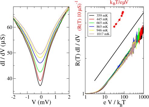
We now focus on the conductance at low voltage (below 0.12 V) which exhibits a pronounced dip at zero bias. This behavior is characteristic of Coulomb blockade through a small capacitance tunnel junction in series with a dissipative electromagnetic environment which can exchange energy with the tunneling quasi particles on a scale much smaller than the charging energy. This yields the so called Dynamical Coulomb Blockade (DCB) ingold . The differential conductance data is expected to follow a scaling behavior as a function of bias and temperature:
| (2) |
with and , and the exponent is expected to be inthe case of Two asymmetric junctions, where R is the resistance of the environment and is the resistance quantum. The data shown in fig.2 yields z of the order of . Such a power law dependence also was found in the two other thicker samples, with similar exponents. It is thus reasonable to assume that the dissipative ohmic environment in the present case is constituted by the few top graphene layers of the graphite samples. Note also that a similar behavior was already observed on multiwall carbon nanotubes with low conductance contacts bachtold .
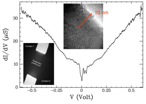
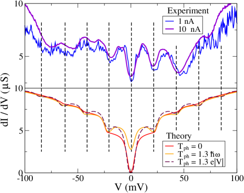
More original, as shown on fig. 3, is the bias dependence of the differential conductance measured on the thinest sample investigated which is 10 nm thick and contains thirty graphene layers. It exhibits a series of eight sharp dips resembling the zero bias one and nearly equally spaced by . Their amplitude decreases with increasing voltage except for the broader dip at 50 mV which can be decomposed into 2 overlapping negative peaks centered around 40 and 60mV as suggested by the data taken at 1nA ac excitation. The energy scale of 20 meV does not correspond to any simple electronic energy scale in the sample, whose charging energy is in the meV range and level spacing in the range. On the other hand the lowest energy optical phonon in graphite (so called Z0’) has an energy of 15meV rubio . This mode, which emerges from the out of plane transverse acoustic mode of graphene rubio ; xray , is only present in graphite and corresponds to the two neighboring, non equivalent, planes vibrating in phase opposition along the c axis. This phonon mode has been observed experimentally in graphite by inelastic X-ray scattering xray and scanning tunneling spectroscopy vitali with an energy of . The observed peak positions at multiple values of 20 mV instead of 15 mV can be attributed to the asymmetry of the contacts which corresponds to the parameter in eq.1. These dips are only observed on the 10 nm thick foil and were not detected on the two thicker (more than 100 nm) samples. This can be understood considering that the conversion from electric energy (depending only on the resistance of the tunneling barriers) into mechanical vibrations leads to an induced vibration amplitude inversely proportional to the number of layers in the graphite foil. The suspended character of the sample is also essential, since interaction with a substrate suppresses considerably the amplitude of induced vibrations as already demonstrated on carbon nanotubes dekkervib . Note that STM spectroscopy on bulk graphite vitali also reveals inelastic contributions due to plasmons which are not detected in the present experiment.
In order to explain the data more quantitatively we extended the work of Mitra et al. mitra04 on the phonon assisted Coulomb staircase observed in the transport through fullerenes molecules. The coupling between the ZO’-phonon mode and the electrons in the graphite sample is described using a Holstein Hamiltonian Holstein . In the absence of disorder this Hamiltonian reads:
| (3) |
where and are the fermionic electron creation and annihilation operators in momentum space, the electronic energy, and and the creation and annihilation operators of the bosonic ZO’-phonon of frequency . In contrast with previous work mitra04 , the electronic energy level spacing is small compared to the phonon energy . The parameter is the dimensionless electron phonon coupling constant which we assume to be of the order of unity like in carbon nanotubes lambda . The coupling to the leads is then described in a dynamical Coulomb-blockade formalism ingold , by a Hamiltonian of the form . Here are the electron annihilation operators in the leads, are the tunnel amplitudes and is a phase operator describing the electromagnetic environment of the junction.
The Hamiltonian can be diagonalized with a canonical Lang-Firsov transformation: , where . In the limit when the charging energy of the sample is negligible mitra04 the transformed Hamiltonian reads simply where we have omitted the primes for the transformed operators. In the transformed basis the transfer Hamiltonian is given by :
| (4) |
This expression is obtained by expanding the product under the assumption that the environment phase commutes with the phonon operators. It shows that the coupling to phonons essentially changes the phase operator of the junction. As a result the current through the junction can be expressed with an effective function describing the probability of electrons to loose an energy in a tunnel transition as in usual DCB theory. Since the electromagnetic environment and phonon operators commute, this function can be expressed as a convolution
| (5) |
where is the probability of emitting a photon of energy in the environment of the junction and is the probability of emitting a phonon in the sample. The probability distribution can be obtained by noticing that the corresponding phase operator is analogous to that of an electromagnetic circuit with resonant frequency ingold (this result can also be obtained directly by tracing out the phonon degrees of freedom in eq.4):
| (6) |
where is the inverse of the phonon temperature . Using Eqs. (5 and 6) and standard expressions for current as a function of ingold it is possible to compute the current through the sample. For example in the case of symmetric contacts () and constant density of states, where is the tunnel resistance of each contact. Note the similarity with the DCB in a tunnel junction in series with a LC resonator devoret95 . The case of an energy dependent density of states , and of asymmetric contacts can readily be included by straightforward generalization of this expression according to eq.1. For comparison with the experiments we assume that the density of states of graphite is of the form: . This formula is exact for bilayer graphene with Bilayer and . We also take the values of , environment resistance and charging energy deduced from the geometry and conductance data at low bias. The only free adjustable parameter is . As shown on fig.3 the agreement with experimental data is only qualitative especially at zero temperature , where theory predicts zero conductance at zero bias which is not observed experimentally . Better agreement is found when a finite phonon temperature is introduced. Since the sample is suspended the populations of phonons are supposed to be strongly out of equilibrium. We have tentatively introduced a phonon temperature increasing linearly with bias which leads to better agreement with experimental data. However, surprisingly, the best fit is obtained by imposing a bias-independent phonon temperature which does not seem a priori very physical. We have also in our model neglected the electronic temperature which is expected to be in the K range. Moreover we have not included the expected broadening of the phonon modes (even at very low temperature) due to the strong coupling to electrons. This may explain why the best fit corresponds to a finite phonon temperature.
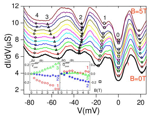
In the following we discuss the magnetic field dependence of the dips in the differential conductance ( fig. 4). They vary both in amplitude and position between 0 and 5 T . Whereas the first two dips and the forth one are shifted toward lower frequency with increasing magnetic field (as seen both at positive and negative bias) the third peak is shifted toward high frequency (we consider here the negative bias data since the second and third dips at positive bias can barely be resolved as discussed above). The amplitude of the dips (see inset in fig.4) may decrease or increase with magnetic field (peak 2 and 3), or vary in a non monotonic way (peak 0 and 1). The relative shifts of the dips with magnetic field by an typical amount of 5 to 20 are of the same order of magnitude as the relative variations of their magnitudes. We attribute these effects to the field dependent density of states of the graphite foil in the field range where Shubnikov de Haas oscillations just start to show up. Even if these observations are not yet understood in detail they indicate a strong electron phonon coupling and justify the value of since a relationship such as between the typical phonon frequency magnetic dependence and magneto conductance, is expected to hold fuchs . High electron phonon coupling has already been reported in graphene concerning in plane optical modes castroneto07 . In the present case however, strong electron phonon coupling between transverse ZO’ vibrations and strongly anisotropic transport in the thin graphite layer is not straight-forward but can be understood if the electrical contacts between the two electrodes and the graphite foil take place through distinct graphene mono-layers which is highly probable.
In conclusion we have shown evidence of differential conductance sharp dips in a suspended thin layer of graphite with 30 graphene foils. These dips can be interpreted within a simple model of dynamical Coulomb blockade with an environment strongly coupled to the lowest energy optical phonon mode ZO’ of graphite. The magnetic field dependence of the effect corroborates this interpretation.
Aknowlegments: We aknowledge M. Kociak for the transmission electron microscopy pictures, J.N.Fuchs and M.Goerbig for fruitful discussions on the electron-phonon coupling in graphite.
References
- (1) A. Levy Yeyati and J.M. van Ruitenbeek, Les Houches Session LXXXI ”Nanophysics: Coherence and Transport”, H. Bouchiat et al., eds. (Elsevier, Amsterdam, 2005) 495-535. O. Tal, M. Krieger, B. Leerink, and J.M. van Ruitenbeek, Phys. Rev. Lett. 100 (2008).
- (2) J. Park, A.N. Pasupathy, J.I. Goldsmith, C. Chang, Y. Yaish, J.R. Petta, M. Rinkoski, J.P. Sethna, H. Abruna, P.L. McEuen, and D.C. Ralph, Nature 17, 722 (2002) H. Park, J. Park, A.K.L. Lim, E.H. Anderson, A.P. Alivisatos, and P.L. McEuen, Nature 407, 57 (2000).
- (3) B. J. LeRoy, S. G. Lemay, J. Kong and C. Dekker, Nature 432, 372(2004).
- (4) S. Sapmaz, P. Jarillo-Herrero, Ya.M. Blanter, C. Dekker, and H. S. J. van der Zant Phys.Rev.Lett.96, 026801 (2006).
- (5) Karsten Flensberg, Phys. Rev. B 68, 205323 (2003).
- (6) Stephan Braig and Karsten Flensberg, Phys. Rev. B 68, 205324 (2003).
- (7) A. Mitra, I. Aleiner, and A. J. Millis Phys.Rev B 69, 245302 (2004).
- (8) L. Wirtz and A.Rubio Solid State Comm. 131 ,141(2004).
- (9) G.L. Ingold and Y.V. Nazarov, in “Single Charge Tunneling”, edited by H. Grabert and MH Devoret, NATO ASI, Ser. B, Vol. 294 (Plenum, New York, 1991), cond-mat/0508728
- (10) T.Holtz, C.Urbina,D.ESteve and M. Devoret Phys.Rev.Lett.73, 3455 (1995).
- (11) P.R. Wallace, Phys.Rev 71,622 (1947).
- (12) A. Bachtold, M. de Jonge, K. Grove-Rasmussen, P. L. McEuen, M. Buitelaar, and C. Sch nenberger, Phys. Rev. Lett. 87, 166801 (2001).
- (13) M. Mohr, J. Maultzsch, E. Dobard ic, S. Reich, I. Milo evic, M. Damnjanovic, A. Bosak, M. Krisch, and C. Thomsen Phys. Rev. B 76, 035439 (2007)
- (14) L.Vitali et al. Phys.Rev B 69, 12141 (2004)
- (15) T. Holstein, Ann. Phys. N.Y. 8, 325 (1959); 8, 343 (1959)
- (16) M.S. Dresselhaus, G. Dresselhaus, and P.C. Eklund, Science of Fullerenes and Carbon Nanotubes Academic Press, San Diego, (1996).
- (17) T. Ando Jour. of Phys. Soc. of Japan 76, 104711 (2007)
- (18) J.N. Fuchs (private communication).
- (19) A.H. Castro Neto and Franciso Guinea, Phys. Rev. B 75, 045404 (2007).