Anisotropic tunneling magnetoresistance and tunneling anisotropic magnetoresistance: spin-orbit coupling in magnetic tunnel junctions
Abstract
The effects of the spin-orbit interaction on the tunneling magnetoresistance of ferromagnet/semiconductor/normal metal tunnel junctions are investigated. Analytical expressions for the tunneling anisotropic magnetoresistance (TAMR) are derived within an approximation in which the dependence of the magnetoresistance on the magnetization orientation in the ferromagnet originates from the interference between Bychkov-Rashba and Dresselhaus spin-orbit couplings that appear at junction interfaces and in the tunneling region. We also investigate the transport properties of ferromagnet/semiconductor/ferromagnet tunnel junctions and show that in such structures the spin-orbit interaction leads not only to the TAMR effect but also to the anisotropy of the conventional tunneling magnetoresistance (TMR). The resulting anisotropic tunneling magnetoresistance (ATMR) depends on the absolute magnetization directions in the ferromagnets. Within the proposed model, depending on the magnetization directions in the ferromagnets, the interplay of Bychkov-Rashba and Dresselhaus spin-orbit couplings produces differences between the rates of transmitted and reflected spins at the ferromagnet/seminconductor interfaces, which results in an anisotropic local density of states at the Fermi surface and in the TAMR and ATMR effects. Model calculations for Fe/GaAs/Fe tunnel junctions are presented. Furthermore, based on rather general symmetry considerations, we deduce the form of the magnetoresistance dependence on the absolute orientations of the magnetizations in the ferromagnets.
pacs:
73.43.Jn, 72.25.Dc, 73.43.QtI Introduction
The tunneling magnetoresistance (TMR) effect is observed in ferromagnet/insulator/ferromagnet heterojunctions, in which the magnetoresistance exhibits a strong dependence on the relative magnetization directions in the two ferromagnetic layers and on their spin polarizations.Jullierè (1975); Maekawa et al. (2002); Slonczewski (1989); Žutić et al. (2004); Fabian et al. (2007) Because of this peculiarly strong asymmetric behavior of the magnetoresistance, TMR devices find multiple uses ranging from magnetic sensors to magnetic random access memory applications.Maekawa et al. (2002); Žutić et al. (2004)
Beyond the conventional TMR effect, it has been observed that the magnetoresistance in magnetic tunnel junctions (MTJs) may also depend on the absolute orientation of the magnetizations in the ferromagnetic leads.Gould et al. (2004); Rüster et al. (2005); Saito et al. (2005); Brey et al. (2004) This phenomenon is called the tunneling anisotropic magnetoresistance (TAMR) effect.Gould et al. (2004); Brey et al. (2004) A theoretical investigation of the tunneling magnetoresistance in GaMnAs/GaAlAs/GaMnAs tunnel junctions was reported in Ref. Brey et al., 2004 which predicted that, as a result of the strong spin-orbit interaction the tunneling magnetoresistance depends on the angle between the current flow direction and the orientation of the electrode magnetization. A difference between the tunneling magnetoresistances in the in-plane (i.e., magnetization in the plane of the magnetic layers) and out-of-plane configurations of up to was predicted for large values of the electrode spin polarization.Brey et al. (2004) Here we refer to this phenomenon as the out-of-plane TAMR. Recent first principles calculations in Fe/MgO/Fe magnetic tunnel junctions (MTJs) predict an out-of-plane TAMR ratio of about 44 %.Khan et al. (2008) On the other hand, we refer to an in-plane TAMR effect as the change in the magnetoresistance when the in-plane magnetization of the ferromagnetic layer(s) is rotated in the plane perpendicular to the direction of the current flow.
It is remarkable that the TAMR is present even in MTJs in which only one of the electrodes is magnetic and the conventional TMR is absent. In contrast to the conventional TMR-based devices, which require two magnetic layers for their operation, TAMR-based devices can operate with a single magnetic lead, opening new possibilities and functionalities for the operation of spintronic devices. The TAMR may also affect the spin-injection from a ferromagnet into a non-magnetic semiconductor. Therefore, in order to correctly interpret the results of spin injection experiments in a spin-valve configuration, it is essential to understand the nature, properties, and origin of the TAMR effect.
The first experimental observation of TAMR was in (Ga,Mn)As/AlOx/Au heterojunctions, in which an in-plane TAMR ratio of about was found.Gould et al. (2004) Experimental investigations of the in-plane TAMR in (Ga,Mn)As/GaAs/(Ga,Mn)As and in (Ga,Mn)As/ZnSe/(Ga,Mn)As tunnel junctions, in which both electrodes are ferromagnetic have also been reported.Rüster et al. (2005); Saito et al. (2005) In the case of (Ga,Mn)As/ZnSe/(Ga,Mn)As, the in-plane TAMR ratio was found to decrease with increasing temperature, from about at 2 K to at 20 K.Saito et al. (2005) This temperature dependence of the in-plane TAMR is more dramatic in the case of (Ga,Mn)As/GaAs/(Ga,Mn)As, for which a TAMR ratio of the order of a few hundred percent at 4 K was amplified to at 1.7 K.Rüster et al. (2005) This huge amplification of the in-plane TAMR was suggested to originate from the opening of the Efros-Shklovskii gapEfros and Shklovskii (1975) at the Fermi energy when crossing the metal-insulator transition.Rüster et al. (2005) Measurements of the TAMR in (Ga,Mn)As/-GaAs Esaki diode devices have also been reported.Ciorga et al. (2007) In addition to the investigations involving vertical tunneling devices the TAMR has also been studied in break junctions,Bolotin et al. (2006); Burton et al. (2007) nanoconstrictionsGiddings et al. (2005); Ciorga et al. (2007) and nanocontacts.Jacob et al. (2008)
Beyond the area of currently low Curie temperature ferromagnetic semiconductors, the TAMR has recently been experimentally investigated in Fe(001)/vacuum/bcc-Cu(001) tunnel junctions, Chantis et al. (2007) Fe/GaAs/Au MTJs,Moser et al. (2007); Fabian et al. (2007) Co/AlOx/Au MTJs,Liu et al. (2008), CoPt structuresShick et al. (2006) and in multilayer-(Co/Pt)/AlOx/Pt structures.Park et al. (2008)
In what follows we focus our discussion on the case of the in-plane TAMR (for brevity we will refer to it as the TAMR effect). We investigate the TAMR in ferromagnet/semiconductor/normal metal (F/S/NM) and in ferromagnet/semiconductor/ferromagnet (F/S/F) MTJs. We propose a model in which the two-fold symmetric magnetoresistance dependence on the orientation of the in-plane magnetization in the ferromagnetic layer(s) originates from the interference of Dresselhaus and Bychkov-Rashba-like spin-orbit couplings. Such interference effects have already been investigated in lateral transport in 2D electron systemsTrushin and Schliemann (2007); Cheng et al. (2007); Chalaev and Loss (2008), in spin relaxation in quantum wells Averkiev and Golub (1999) and quantum dots Stano and Fabian (2006), or in 2D plasmons.Badalyan et al. (2008) The symmetry, which is imprinted in the tunneling probability becomes apparent when a magnetic moment is present. Our main results are: i) finding analytical expressions for evaluating the TAMR in both F/S/NM and F/S/F MTJs, ii) prediction and evaluation of the ATMR in F/S/F heterojunctions, and iii) derivation of a simple phenomenological relation describing the dependence of the tunneling magnetoresistance on the absolute orientation of the magnetization(s) of the ferromagnet(s).
The paper is organized as follows. In Sec. II we present the theoretical model describing the tunneling through a MTJ. In a first approximation we consider the case of an infinitesimally thin barrier (Sec. II.1), while the finite spatial extension of the potential barrier is incorporated in a more sophisticated approach discussed in Sec. II.2. Detailed solutions and tunneling properties within these approximations are given in Appendices A and B, respectively. In Sec. III we discuss the TAMR in both F/S/NM (Sec. III.1) and F/S/F (Sec. III.2) MTJs. The ATMR in F/S/F tunnel junctions is investigated in Sec. IV, where specific calculations for model Fe/GaAs/Fe MTJs are presented. In Sec. V we develop a phenological model for determining the dependence of the TAMR and ATMR on the absolute orientation(s) of the magnetization(s) in the ferromagnetic lead(s). Finally, conclusions are given in Sec. VI.
II Theoretical model.
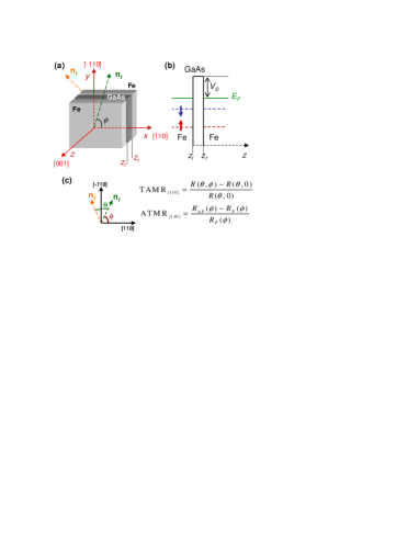
Consider a F/S/F tunnel heterojunction. The semiconductor is assumed to lack bulk inversion symmetry (zinc-blende semiconductors are typical examples). The bulk inversion asymmetry of the semiconductor together with the structure inversion asymmetry (for the case of asymmetric junctions) of the heterojunction give rise to the DresselhausDresselhaus (1955); Rössler and Kainz (2002); Winkler (2003); Fabian et al. (2007) and Bychkov-RashbaBychkov and Rashba (1984); Winkler (2003); Fabian et al. (2007) SOIs, respectively. The interference of these two spin-orbit couplings leads to a net anisotropic SOI with a symmetry which is imprinted onto the tunneling magnetoresistance as the electrons pass through the semiconductor barrier. This was discussed in some details in Refs. Moser et al., 2007; Fabian et al., 2007 for the case of F/S/NM tunnel junctions. Here we generalize the model proposed in Refs. Moser et al., 2007; Fabian et al., 2007 to the case of F/S/F tunnel junctions. For such structures our model predicts the coexistence of both the TAMR and ATMR phenomena.
We consider a F/S/F tunnel junction grown in the direction, where the semiconductor forms a barrier of width between the left and right ferromagnetic electrodes. At first we discuss a simplified model for very thin barriers. In that case the barrier can be approximated by a Dirac delta function and the SOI reduced to the plane of the barrier. In what follows we will refer to this model as the Dirac delta model (DDM). A second model in which Slonczewski’s proposalSlonczewski (1989); Fabian et al. (2007) for ferromagnet/insulator/ferromagnet tunnel junctions is generalized to the case of ferromagnet/semiconductor/ferromagnet junctions by including the Bychkov-Rashba and Dresselhaus SOIs will be referred to as the Slonczewski spin-orbit model (SSOM).
II.1 Dirac delta model (DDM)
We consider here the case of a very thin tunneling barrier. Assuming that the in-plane wave vector is conserved throughout the heterostructure, one can decouple the motion along the growth direction () from the other spatial degrees of freedom. The effective model Hamiltonian describing the tunneling across the heterojunction reads
| (1) |
Here
| (2) |
with the bare electron mass, and and the high and width, respectively, of the actual potential barrier [here modelled with a Dirac delta function ] along the growth direction () of the heterostructure.
The spin splitting due to the exchange field in the left and right ferromagnetic regions is given by
| (3) |
Here and represent the exchange energy in the left and right ferromagnets, respectively, and is the Heaviside step function. The components of the vector are the Pauli matrices, and with is a unit vector defining the in-plane magnetization direction in the left () and right () ferromagnets with respect to the [100] crystallographic direction. The Zeeman splitting in the semiconductor can be neglected.
We note that in recent experiments with Fe/GaAs/Au tunnel junctions,Moser et al. (2007) the reference axis was taken as the [110] direction. Therefore, it is convenient to express the magnetization direction relative to the [110] axis by introducing the angle shifting (). One can then write with giving the magnetization direction in the left () and right () ferromagnets with respect to the [110] crystallographic direction.
Within the DDM, the spin-orbit interaction throughout the semiconductor barrier (including the interfaces) can be written as
| (4) |
with the effective spin-orbit coupling field
| (5) |
Here and represent effective values of the Bychkov-Rashba and linearized Dresselhaus parameters, respectively, and and refer to the and components of the wave vector . In terms of the usual Dresselhaus parameter , the linearized Dresselhaus parameter can be approximatedFabian et al. (2007) as , where stands for the strength of the effective wave vector in the barrier.
The scattering states in the left () and right () ferromagnetic regions are given by
| (6) |
and
| (7) |
respectively. Here we have introduced the wave vector components
| (8) |
and
| (9) |
with denoting the length of the wave vector component corresponding to the free motion in the plane. The spinors
| (10) |
correspond to a spin parallel () or antiparallel () to the magnetization direction in the left () and right () ferromagnets.
The reflection and transmission coefficients can be found by imposing appropriate boundary conditions and solving the corresponding system of linear equations (for details see Appendix A). The transmissivity of an incoming spin- particle can then be evaluated from the relation
| (11) |
Explicit analytical expressions for the transmission coefficients and are given in Appendix A.
II.2 Slonczewski spin-orbit model (SSOM)
We give a generalization of the Slonczewski modelSlonczewski (1989) for ferromagnet/insulator/ferromagnet tunnel junctions to the case in which the insulator barrier is replaced by a zinc-blende semiconductor. Unlike in the DDM, now the spatial extension of the potential barrier is taken into account. The model Hamiltonian is
| (12) |
where
| (13) |
The electron effective mass is assumed to be in the central (semiconductor) region and in the ferromagnets. The exchange splitting in the ferromagnets is now given by
| (14) |
The Dresselhaus SOI can be written asRössler and Kainz (2002); Winkler (2003); Ganichev et al. (2004); Zawadzki and Pfeffer (2004); Fabian et al. (2007)
| (15) |
where and correspond to the and directions, respectively. The Dresselhaus parameter has a finite value in the semiconductor region, where the bulk inversion asymmetry is present, and vanishes elsewhere. Note that because of the step-like spatial dependence of , the Dresselhaus SOI [Eq. (15)] implicitly includes both the interface and bulk contributions.Rössler and Kainz (2002); Zawadzki and Pfeffer (2004); Fabian et al. (2007)
The Bychkov-Rashba SOI is given bynot (a)
| (16) |
and arises due to the ferromagnet/semiconductor interface inversion asymmetry.Fabian et al. (2007) Here () denotes the SOI strength at the left (right) interface (). For the small voltages considered here (up to a hundred mV), the Bychkov-Rashba SOI inside the semiconductor can be neglected.
The -components of the scattering states in the left and right ferromagnets have the same form as in Eqs. (6) and (7), respectively.
In the central (semiconductor) region () we have
| (17) |
| (18) |
The angle is defined through the relation . We have also used the notation
| (19) |
where
| (20) |
is the length of the component of the wave vector in the barrier in the absence of SOI.
The expansion coefficients in Eqs. (6), (7), and (17 can be found by applying appropriate matching conditions at each interface and by solving the corresponding system of linear equations (for details, see Appendix B). Once the wave function is determined, the particle transmissivity can be calculated from Eq. (11). Approximate analytical expressions for the transmission coefficients and are given in Appendix B.
III Tunneling anisotropic magnetoresistance (TAMR)
The magnetoresistance of a tunnel junction can be obtained by evaluating the current through the device or the conductance. The current flowing along the heterojunction is given by
| (21) |
where and are Fermi-Dirac distributions with chemical potentials and in the left and right (metallic or ferromagnetic) leads, respectively. For the case of zero temperature and small voltages, the Fermi-Dirac distributions can be expanded in powers of the voltage . To first order in one obtains with the Dirac delta function and the Fermi energy. One then obtains the following approximate expression for the conductance
| (22) |
We note that although similar, the expression above differs from the linear response conductance. In our case, the transmissivity depends on the Bychkov-Rashba parameter . Recent first-principles calculationsGmitra et al. (2008) have shown that the spin-orbit coupling field is different for different bands, therefore the effective value of is energy dependent. By applying an external voltage the energy window relevant for tunneling can be changed, resulting in voltage-dependent values of . Consequently, the conductance in Eq. (22) depends, parametrically, on the applied voltage.
III.1 TAMR in ferromagnet/semiconductor/normal metal tunnel junctions
The tunneling properties of F/S/NM junctions can be obtained as a limit case of the models proposed in Sec. II for F/S/F tunnel junctions by taking and as the Zeeman splitting in the normal metal region. In the present case , , and refer to the ferromagnetic (left), semiconductor (central), and normal metal (right) regions, respectively.

The TAMR in F/S/NM tunnel junctions refers to the changes of the tunneling magnetoresistance () when varying the magnetization direction of the magnetic layer with respect to a fixed axis. Here we assume the [110] crystallographic direction as the reference axis. The TAMR is then given byFabian et al. (2007)
| (23) |
Since in a F/S/NM tunnel junction only one electrode is magnetic, the conventional TMR effect is absent.
An alternative to the magnetoresistance, which refers to the charge transport, is the spin polarization efficiency of the transmission characterized by the tunneling spin polarizationMaekawa et al. (2002); Žutić et al. (2004)
| (24) |
where is the charge current corresponding to the spin- channel and is the total current. The changes in the tunneling spin polarization when the magnetization of the ferromagnet is rotated in-plane can then be characterized by the tunneling anisotropic spin polarization (TASP), which is defined asFabian et al. (2007)
| (25) |
Taking into account that the Zeeman splitting in the normal metal is small we can approximate . Then for the DDM the conductance is given by Eq. (80). It follows from Eqs. (23) and Eq. (80) that the TAMR is given by
| (26) |
For junctions in which the Bychkov-Rashba and Dresselhaus SOIs can be considered as small perturbations, the anisotropy is small and . In addition, the spin-orbit contribution [see Eqs. (69)-(71)]) to the isotropic part of the conductance is also much smaller than the contribution , corresponding to the system in the absence of the SOI, i.e., . Therefore one can drop the contributions and from the denominator in Eq. (26). The TAMR can then be approximated as
| (27) |
The substitution of Eq. (78) into Eq. (27) leads to
| (28) |
Here we have introduced the dimensionless SOC parameters and . The functions and are given by Eq. (79).
The expression above gives the angular dependence of the TAMR and is consistent with the angular dependence experimentally observed in Fa/GaAs/Au tunnel junctions.Moser et al. (2007) It also suggests that bias-induced changes of the sign of the Bychkov-Rashba parameter result in the inversion (change of sign) of the TAMR (such an inversion has been experimentally observed.Moser et al. (2007)) Furthermore, one can see from Eq. (III.1) that the amplitude of the TAMR is governed by the product and the averages (). When , the two-fold TAMR is suppressed (the suppression of the TAMR was also observed in Ref.Moser et al., 2007), i.e., as long as other anisotropic effects such as uniaxial strain are not present, the Bychkov-Rashba (or Dresselhaus) SOI alone cannot explain the experimentally observed symmetry of the TAMR. The TAMR vanishes also if the spin polarization of both electrodes becomes sufficiently small. In such a case and vanishes [see Eq. (79)], resulting in the suppression of the TAMR. On the contrary, Eq. (III.1) predicts an increase of the TAMR amplitude for F/S/NM tunnel junctions whose constituents exhibit large values of as well as a large spin polarization in the magnetic electrode.
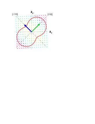
A simple, intuitive explanation of the origin of the uniaxial anisotropy of the TAMR can be obtained by investigating the dependence of the effective spin-orbit coupling field [see Eq. (5)], i.e., the effective magnetic field that the spins feel when traversing the semiconducting barrier. A schematics of the anisotropy of the spin-orbit field is shown in Fig. (2), where the thin arrows represent a vector plot of , while the solid line is a polar plot of the field amplitude for a fixed value of . The spin-orbit field is oriented in the [110] ([-110]) direction at the points of low (high) spin-orbit field, where the field amplitude reaches a minimum (maximum). When the magnetization in the ferromagnet points along the [-110] direction, the direction of the highest spin-orbit field is parallel to the incident, majority spins which are then easily transmitted through the barrier. On the other hand, for a magnetization direction [110], the highest spin-orbit field is perpendicular to the incident spins (to both the majority and minority spins) and the transmission becomes less favorable than in the case the magnetization is in the [-110] direction. This spin-orbit induced difference in the tunneling transmissivities depending on the magnetization direction results in the uniaxial anisotropy of the TAMR.not (b) Furthermore, the magnetization direction dependence of the transmission and reflection of the incident spins should be reflected in the local density of states at the interfaces of the barrier. Within the DDM the left (F/S) and right (S/NM) interfaces are merged into a single plane and one can not distinguish between them. A more detailed view of the role of the interfaces requires the use of the SSOM. It turns out (this will be shown latter in this section) that the F/S interface plays a major role in the TAMR phenomenon while the S/NM interface appears irrelevant. This is intuitively expected since the exchange splitting in the ferromagnet is much larger than the Zeeman splitting in the normal metal. Consequently, the spin-valve effect at the F/S interface is much stronger than in the S/NM interface.
The local density of states reflect also the uniaxial anisotropy of the TAMR with respect to the magnetization orientation in the ferromagnet. In fact, one can introduce the anisotropic, local density of states (ALDOS) through the definition
| (29) |
where
| (30) |
is the total local density of states at position and evaluated at the Fermi surface determined by the Fermi wave vectors
| (31) |
Since we are interested only in propagating states, we may restrict the possible values of to the interval , with given by Eq. (77). Since the spin splitting in the normal metal region is negligibly small, . It follows from Eqs. (7) and (11) that
| (32) |
and, therefore, the conductance [see Eq. (22)] is related to the LDOS at as . One then obtains that
| (33) |
For a numerical illustration we consider an epitaxial Fe/GaAs/Au heterojunction similar to that used in the experimental observations reported in Ref. Moser et al., 2007. We use the value for the electron effective mass in the central (GaAs) region. The barrier width and hight (measured from the Fermi energy) are, respectively, and , corresponding to the experimental samples in Ref. Moser et al., 2007. For the Fe layer a Stoner model with the majority and minority spin channels having Fermi momenta and , Wang et al. (2003) respectively, is assumed. The Fermi momentum in Au is taken as . Ashcroft and Mermin (1976) We consider the case of relatively weak magnetic fields (specifically, ). At high magnetic fields, say, several Tesla, our model is invalid as it does not include cyclotron effects which become relevant when the cyclotron radius approaches the barrier width.
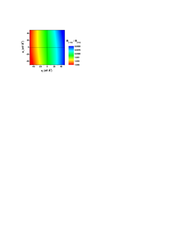
The Dresselhaus spin-orbit parameter in GaAs is .Winkler (2003); Ganichev et al. (2004); Fabian et al. (2007) On the other hand, the values of the interface Bychkov-Rashba parameters , [see Eq. (16)] are not know for metal-semiconductor interfaces. Due to the complexity of the problem, a theoretical estimation of such parameters requires first-principles calculations including the band structure details of the involved materials,Gmitra et al. (2008) which is beyond the scope of the present paper. Here we assume and as phenomenological parameters which must be understood as the values of the interface Bychkov-Rashba parameters at the ferromagnet/semiconductor and semiconductor/normal metal interfaces, respectively, averaged over all the relevant bands contributing to the transport across the corresponding interfaces. In order to investigate how does the degree of anisotropy depend on these two parameters we performed calculations of the ratio (which is a measure of the degree of anisotropyMoser et al. (2007)) as a function of and by using the spin-orbit Slonczewski model described in Sec. II.2. The results are shown in Fig. 3, where one can appreciate that the size of this ratio (and, consequently, of the TAMR) is dominated by . This is because the Zeeman splitting in Au is very small compared to the exchange splitting in Fe and, consequently, the spin flips mainly when crossing the ferromagnet/semiconductor interface. Then, since the values of the TAMR are not very sensitive to the changes of we can set this parameter, without loss of generality, to zero. This leaves as a single fitting parameter when comparing to experiment. The values of the phenomenological parameter were determined in Refs. Moser et al., 2007; Fabian et al., 2007 by fitting the theory to the experimental value of the ratio and a very satisfactory agreement between theory and experiment was achieved. This fitting at a single angle was enough for the theoretical model to reproduce the complete angular dependence of the TAMR, demonstrating the robustness of the model.
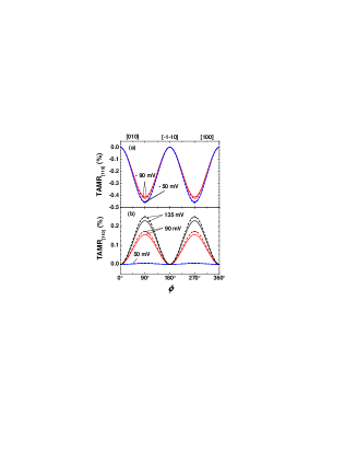
Assuming that the interface Bychkov-Rashba parameter is voltage dependent and performing the fitting procedure for different values of the bias voltage the bias dependence of can be extracted.Moser et al. (2007); Fabian et al. (2007) Here we use the same values of reported in Refs. Moser et al., 2007; Fabian et al., 2007 for computing the angular dependence of the TAMR at different values of the bias voltage. The results are shown in Fig. 4, where the dashed and solid lines correspond to calculations within the DDM and the SSOM, respectively. An overall agreement between the two models can be appreciated. The TAMR exhibits an oscillatory behavior as a function of the magnetization direction [see also Eq. (III.1)] and can be inverted by changing the bias voltage [compare Figs. 4(a) and (b)]. This bias induced inversion of the TAMR was experimentally observed in Fe/GaAs/Au tunnel junctionsMoser et al. (2007) and was explained to occur as a consequence of a bias induced change in the sign of the effective Bychkov-Rashba parameter. Preliminary ab initio calculationsGmitra et al. (2008) for Fe/GaAs structures suggest that the Bychkov-Rashba parameters associated with different bands may have different values and even change the sign. Thus, the effective value of the interface Bychkov-Rashba parameter will depend on which bands are the ones that mainly contribute to the transport across the Fe/GaAs interface (at low temperature those are the ones which have the appropriate symmetry and lie inside the voltage window around the Fermi energy). For different values of the bias voltage different set of bands will be relevant to transport. On the other hand, to different set of bands correspond different effective values of the interface Bychkov-Rashba parameter. Consequently, becomes strongly dependent on the bias voltage. The above analysis leads to the conclusion that the inversion of the TAMR originates from the bias induced sign change of the effective Bychkov-Rashba SOI at the Fe/GaAs interface, as proposed in Refs. Moser et al., 2007; Fabian et al., 2007.
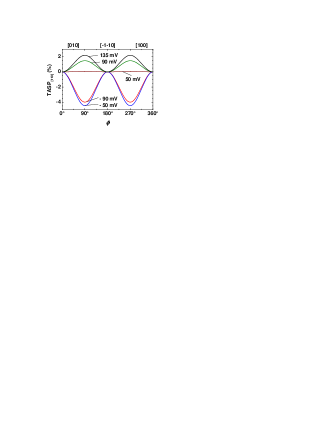
The sign change of the effective Bychkov-Rashba parameter has also influence on the tunneling spin polarization, resulting in the bias induced inversion (change of sign) of the TASP as shown in Fig. 5. Bias induced changes of the sign of the tunneling spin polarization in Fe/GaAs/Cu MTJs has also been reported.Chantis et al. (2007) The anisotropy of the tunneling spin polarization, which also exhibits a two-fold symmetry, indicates that the amount of transmitted and reflected spin at the interfaces depends on the magnetization direction in the Fe layer, resulting in an anisotropic local density of states at the Fermi surface. This is consistent with previous worksGould et al. (2004); Rüster et al. (2005); Park et al. (2008) in which the anisotropy of the density of states with respect to the magnetization direction was related to the origin of the TAMR. In fact, our model calculations reveal that the TAMR, ALDOS [see Eq. (33)], and TASP all exhibit a symmetry with the same kind of angular dependence (compare Figs. 4 and 5).
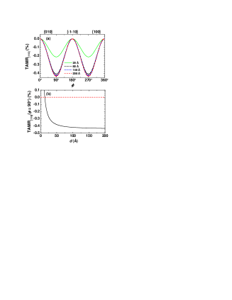
A system parameter that can influence the size of the TAMR is the width of the barrier. The angular dependence of the TAMR calculated within the SSOM for the case of is displayed in Fig. 6(a) for different values of the barrier width . As one would expect, the changes in the barrier width do not affect the two-fold symmetry of the TAMR but only its amplitude, whose absolute value is predicted to increase when increasing the width of the barrier [see Fig. 6(b)].
We remark that our model neglects the contribution of the spin-orbit-induced symmetries of the involved bulk structures. Say, Fe exhibits a four-fold anisotropy, which should be reflected in the tunneling density of states. The fact that this is not seen in the experiment suggests that this effect is smaller than the two-fold symmetry considered in our model.
III.2 TAMR in ferromagnet/semiconductor/ferromagnet tunnel junctions
Our discussion in Sec. III.1 suggests that in the case of a F/S/F tunnel junction, the magnetoresistance will depend on the absolute direction of the magnetization in each of the ferromagnets. In the left and right electrodes, the magnetization directions with respect to the [110] crystallographic direction are given by the angles and , respectively. For convenience we introduce the angle , describing the magnetization direction in the right ferromagnet relative to that in the left ferromagnet (see Fig. 7). Different values of the tunneling magnetoresistance are expected to occur when in-plane rotating the magnetizations of both ferromagnets at the same time, while keeping the relative angle fixed. Thus, the expression for the TAMR in F/S/NM junctions [see Eq. (23)] can now be generalized as
| (34) |
Following the same procedure as in Sec. III.1, one can, in principle, obtain analytical expressions for the TAMR in a F/S/F junction. It turns out however that in the general case defined by Eq. (34) the resulting relations are quite lengthy and not much simpler than the more accurate expressions obtained within the SSOM (see Appendix B). Therefore, we omit here the expressions resulting from the DDM and show only the results obtained within the SSOM.
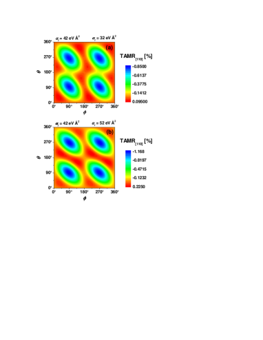
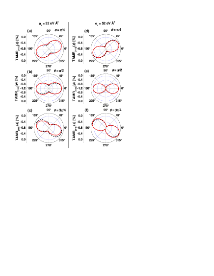
The dependence of the TAMR on the angles and is shown in Fig. 8 for the case of a Fe/GaAs/Fe MTJ. The width of the barrier is Å. Two different cases, corresponding to (a) and (b), are considered. In both cases, the absolute value of the TAMR reaches its maximal amplitude when the magnetization of the left electrode is parallel to the [-110] direction (i.e., ) and the one of the right electrode is perpendicular to it (i.e., ). This is because this configuration, in our parabolic model, corresponds to the case of the stronger structure inversion asymmetry and, consequently, to the largest absolute value of the effective Bychkov-Rashba parameter . We also note that at a fixed value of the TAMR has a two-fold symmetry with respect to and vice versa. It is clear, however, that the angles and play different roles in the symmetry of the TAMR, which manifest in the lack of mirror symmetry with respect to the axis . We have investigated some traces of the TAMR displayed in Fig. 8. The results are shown in Fig. 9 where we present polar plots of the TAMR as a function of for fixed values of . The solid lines correspond to the calculations within the SSOM. The meaning of the dashed lines will be explained in Sec. V. The orientation of the symmetry axis of the two-fold symmetric TAMR is determined by the relative angle rather than by the relative values of the interface Bychkov-Rashba parameters (note for the same , the symmetry axis does not change its orientation with ). The amplitude of the TAMR is bigger for the case of eV Å2 than for eV Å2 and shows a strong dependence on .
IV Anisotropic tunneling magnetoresistance (ATMR)
We now consider the SOI effects on the TMR for the case of a F/S/F tunnel junction. The conventional TMR effect in ferromagnet/insulator/ferromagnet (F/I/F) tunnel junctions relies on the dependence of the magnetoresistance across the junction on the relative magnetization directions in the different ferromagnetic layers and their spin polarizationsSlonczewski (1989); Fabian et al. (2007) and is usually defined as
| (35) |
where () is the magnetoresistance measured when the magnetization of the left and right ferromagnetic layers are parallel (antiparallel).
In the case of F/S/F heterojunctions, the interference between Bychkov-Rashba and Dresselhaus SOIs leads to anisotropic effects. Consequently, the conventional TMR in F/S/F junctions will depend not only on the relative but also on the absolute magnetization directions in the ferromagnets, resulting in an anisotropic magnetoresistance. For quantifying this phenomenon we use the following anisotropic generalization of the TMR,
| (36) |
which now accounts for the magnetoresistance dependence on the absolute magnetization orientations with respect to the [110] crystallographic direction (see Fig. 7). Furthermore, the efficiency of the anisotropic effects on the tunneling magnetoresistance can be defined as
| (37) |
A simplified approximate expression for the ATMR can be found within the DDM by following the same procedure as in Sec. III.1. The result is
| (38) |
where is the conventional TMR in the absence of SOI, and the functions , , , and are given by the Eqs. (87),(88), (A), and (95), respectively. Assuming that the spin-orbit effects on the conventional TMR are small one can approximate the ATMR efficiency as
| (39) |
Note that the angular dependence of the efficiency is similar to that of the TAMR given in Eq. (III.1).
It follows from Eq. (IV) that when both Bychkov-Rashba and Dresselhaus SOIs are present (i.e., when ), the magnetoresistance becomes anisotropic, resulting in the ATMR effect here predicted. One can see also that this effect exhibits a two-fold symmetry with a angular dependence. Unlike the TAMR, when the ATMR becomes isotropic but does not vanish. However, in such a limit the efficiency of the ATMR do vanish [see Eq. (39)], indicating the absence of anisotropy. Like for the TAMR, changes of the sign of result in the inversion (change of sign) of the efficiency of the ATMR. On the other hand, since the TMR contribution in Eq. (IV) is usually the dominant one, the bias-induced changes of the sign of the Bychkov-Rashba parameter will not, in general, cause the inversion (change of sign) of the ATMR. However, the fact that the TMR contribution may change sign in dependence of the applied voltageDe Teresa et al. (1999); Sharma et al. (1999); Moser et al. (2006) can result in the inversion of the ATMR.
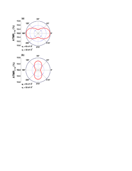
We performed calculations within the SSOM of the angular dependence of the ATMR for a Fe/GaAs/Fe MTJ with a fixed value of the left-interface Bychkov-Rashba parameter ( eV Å2) corresponding to a bias voltage mV . The results are shown in Figs. 10 (a) and (b) for the parameters eV Å2 and eV Å2. The angular dependence of the ATMR is consistent with Eq. (IV). The orientation of the symmetry axis of the ATMR is determined by the sign of the effective value . On the other hand, the amplitude of the ATMR shows a behavior opposite to the one corresponding to the TAMR (see Fig. 9), in the sense that now the amplitude of the anisotropy of the TMR is bigger for the case eV Å2 than for eV Å2 and, unlike for the case of the TAMR (see Fig. 9), the orientation of the symmetry axis of the ATMR can be flipped by varying the value of .
V Phenomenological model of TAMR and ATMR
In order to explain the origin of the angular dependence of the TAMR [see Eq. (III.1)] in F/S/NM junctions, a phenomenological model based on rather general symmetry considerations was proposed in Ref.Moser et al., 2007 and elaborated in more details in Ref.Fabian et al., 2007. Here we extend this phenomenological model to the case of F/S/F tunnel junctions.
For a given , there are three preferential directions in the system: i) the magnetization direction in the left ferromagnet, ii) the magnetization direction in the right ferromagnet, and iii) the direction of the effective spin-orbit field . A scalar quantity such as the transmissivity for the spin channel can be expanded in a series of the all possible scalars one can form with the vectors , , and . Thus, to the second order in , we have
| (40) |
Note that because of symmetry reasons,Fabian et al. (2007) the linear in terms vanishes after averaging over and, therefore, we have omitted them in Eq. (40). The zero order terms have the general form
| (41) |
where and are isotropic expansion coefficients.
Taking into account that and , the general angular dependence of can be extracted from Eq. (41). The result is
| (42) |
This equation describes the dependence of the transmissivity on the relative angle between the magnetizations in the left and right ferromagnetic electrodes in the absence of SOI and is consistent with previous results.Slonczewski (1989); Fabian et al. (2007)
The second order contribution can be cast in the following general form
| (43) | |||||
with the expansion coefficients () being angular independent. To second order in the SOI, the conductance is then given by
| (44) |
where denotes average over and evaluation at the Fermi energy .
Taking into account Eqs. (5), (42), (43), and (44) and performing the corresponding angular averaging in -space one obtains the following, general form of the total conductance ,
| (45) | |||||
where
| (46) |
| (47) |
| (48) |
| (49) |
and
| (50) |
In the equations above the average have the same meaning as in Eq. (76). We note that for systems which are isotropic in the absence of the SOI these equations are quite general. They are valid up to second order in the strength of the spin-orbit coupling field regardless of the specific form of .
One can see that for the case of a F/S/NM junction or for the case of parallel and antiparallel configurations in a F/S/F junction, the general angular dependence given in Eq. (45) is consistent with the corresponding expressions obtained in Appendix A. We want to stress, however, that the relations presented in Appendix A are the result of a specific approximation (the DDM), while Eqs. (45) - (50) are general, and valid for any model or approximation (as far as the system without SOI is isotropic, the effective spin-orbit field is weak, and , , and lie in a plane perpendicular to the current flow). More general relations corresponding to arbitrary orientations of , , and will be given elsewhere.A. Matos-Abiague et al. (2008)
The general form of the TAMR in F/S/NM junctions follows from Eqs. (5), (23) and (45). Proceeding as in Sec. III.1 one finds
| (51) |
which is consistent with the corresponding expression found within the DDM [see Eq. (III.1)]. Similarly, one obtains for the TMR and ATMR in F/S/F junctions the following general expressions,
| (52) |
and
| (53) |
respectively. Note that Eq. (V) is consistent with our previous result in Eq. (IV).
The TAMR in a F/S/F exhibits a more complicated angular dependence, which has the general form
| (54) |
where
| (55) |
and
| (56) |
At the phenomenological level, the expansion constants in Eqs. (45) and (V) can be determined from conductance measurements (or conductance theoretical evaluation) at selected values of and . For example, the values of the phenomenological constants can be determine as follows
| (57) |
| (58) |
| (59) |
| (60) |
and
| (61) |
It is worth noting that although we have referred to the coefficients as constants, strictly speaking, these parameters may exhibit a dependence on the relative angle . Such a dependence may originate from the fact that the averages containing the components of the spin-orbit field [see Eqs. (V) - (50)] are, in principle, -dependent. However, as shown below, this effect is weak for the system here considered.
In order to check the validity of the general angular dependence given in Eqs. (45) and (V) we have computed the expansion coefficients from Eqs. (57) - (61) by using the SSOM. We then evaluate the TAMR by using the phenomenological relation given in Eq. (V) and compare the results (see dashed lines in Fig. 9) with the full angular dependence obtained from the SSOM (solid lines in Fig. 9). The agreement is satisfactory although some small discrepancies appear. We attribute these discrepancies to the fact that when determining the coefficients from Eqs. (57) - (61) we have ignored, as discussed above, that these coefficients are weakly -dependent.
VI Conclusions
We have investigated the spin-orbit induced anisotropy of the tunneling magnetoresistance of F/S/NM and F/S/F MTJs. By performing model calculations we have shown that the two-fold symmetry of the TAMR effect may arise from the interplay of Bychkov-Rashba and Dresselhaus SOIs. The spin-orbit interference effects in F/S/F MTJs lead to the anisotropy of the conventional TMR. Thus, the ATMR depends on the absolute magnetization directions in the ferromagnets. The magnetoresistance dependence on the absolute orientation of the magnetization in the ferromagnets is deduced from general symmetry considerations.
Acknowledgements.
We are grateful to M. Gmitra for useful hints and discussions and to D. Weiss and J. Moser for discussions on TAMR related experiments. This work was supported by the Deutsche Forschungsgemeinschaft (DFG) through the Sonderforschungsbereich (SFB) 689.Appendix A
The eigenfunctions of the Hamiltonian given by Eq. (1) obey the following matching conditions
| (62) |
which, with the scattering states in Eqs.(6) and (7), lead to a system of 4 linear equations for determining the coefficients , , , and . The transmission coefficients are found to be given by
| (63) | |||||
and
| (64) | |||||
where
| (65) |
with
| (66) | |||||
The vectors () are given by
| (67) |
while and .
The transmissivity for an incident particle with spin is given by Eq. (11). For the case of a F/S/NM junction we can approximate and the transmissivity reduces to
| (68) |
In order to obtain a simplified analytical expression for the TAMR in F/S/NM junctions, we consider the case in which the effective spin-orbit field is small. In such a case one can expand Eq. (68) in powers of and obtain the conductance from Eq. (22). The result, up to second order in , reads
| (69) |
The isotropic part of the conductance is given by
| (70) |
where
| (71) |
with
| (72) |
is the conductance in absence of the SOI and
| (73) |
is the isotropic contribution induced by the SOI. Here we have denoted , and
| (74) |
We have also introduced dimensionless SOC parameters as
| (75) |
The function is defined below in Eq. (79). The average
| (76) |
where
| (77) |
denotes the maximum values of for which we have incident and transmitted propagating states. In the average defined in Eq. (76) the corresponding angular integration over [see Eq. (22)] has already been performed.
The spin-orbit induced anisotropy of the conductance is determined by the relation
| (78) |
where
| (79) |
The total conductance can then be written as
| (80) |
with and .
We now consider the case of a F/S/F tunnel junction. For the general case of arbitrary orientations of the magnetization in the left and right ferromagnets, the analytical expressions for the conductance are very lengthy and we therefore omit them here. Simpler expressions are found, however, for the particular cases of parallel (P) and antiparallel (AP) configurations. If we consider that the ferromagnetic electrodes are made of the same material, then and the transmissivity reduces to
| (81) |
Following the same procedure as above, the following expression for the conductance in the parallel configuration is found
| (82) |
The isotropic part is given by
| (83) |
where
| (84) |
and
| (85) |
The anisotropic contribution reads
| (86) |
The functions and are given by
| (87) |
and
| (88) |
respectively.
On the other hand, for the case of antiparallel configuration one obtains the following expressions
| (89) |
where
| (90) |
| (91) |
and
| (92) |
The anisotropic contribution for the antiparallel case reads
| (93) |
and the functions and are given by
| (94) |
and
| (95) |
respectively.
In the derivation of Eqs. (85), (86), (92), and (93) we assumed that the spin orbit parameters and are independent of the relative magnetization orientations in the ferromagnets. Strictly speaking the values of and are -dependent and therefore to the parallel and antiparallel configurations correspond slightly different sets of effective spin orbit parameters. This effect turns out to be negligible for the system here investigated and we therefore omit it.
In both the parallel and antiparallel cases, the averages have the same meaning as in Eq. (76) but now with defined as
| (96) |
It is worth noting that for a junction with structure inversion symmetry the average Bychkov-Rashba parameter vanishes. One may think that since we are considering a structure with leads of the same material the anisotropic term in the conductance corresponding to the parallel configuration (for the parallel configuration the structure becomes symmetric under spatial inversion) will vanishes. This is so for strictly symmetric under spatial inversion structures. In practice, however, the interfaces may not be identical, e.g., one of the interfaces may be epitaxial while the other not. Another possibility is to consider different terminations of the semiconductor at the left and right interfaces. For the case of Fe/GaAs/Fe structures, for example, one of the Fe/Gas interface may be Ga terminated while the other may be As terminated.Erwin et al. (2002); Zega et al. (2006) This interface-induced asymmetry is enough for the average Bychkov-Rashba parameter to have a sizable value.
Appendix B
Here we discuss the details about the solutions of the SSOM and provide approximate expressions for the tunneling coefficients.
By requiring the probability flux conservation across the interfaces one obtains that the eigenfunctions of the Hamiltonian in Eq. (12) should fulfil the following boundary conditions
| (97) |
| (98) | |||||
where and and are the locations of the left and right interfaces, respectively. The interface Bychkov-Rashba parameters are introduced as , , while the Dresselhaus parameter is in the semiconductor and vanishes elsewhere (i.e., ).
Applying the above boundary conditions to the scattering states given in Section II.2 one obtains a system of 8 linear equations for determining the 8 unknown expansion coefficients. The exact expressions for the transmission coefficients and are quite cumbersome. However, simplified analytical expressions for and are found in the limit . In such a case one finds the following approximate relations for the tunneling coefficients,
| (99) |
where , with
| (100) |
and
| (101) |
Furthermore, we have
| (102) |
and
| (103) |
In these equations we introduced the notation
| (104) |
where ,
| (105) |
and
| (106) |
It is worth noting that the approximate expressions for the tunneling coefficients here provided are valid up to first order in . This approximation is appropriate for treating junctions with high and not too thin potential barriers. For the systems here considered the hight of the barrier (with respect to the Fermi level) is about and varies from to . In such cases the approximations here discussed turns out to be excellent.
It is not difficult to show that in the limit , the expressions for the tunneling coefficients here obtained reduce to the ones reported in Ref. Fabian et al., 2007 for the case of vanishing SOI.
We also remark that the expressions above were obtained for the general case of a F/S/F tunnel junction but the corresponding expressions for a F/S/NM junction can easily be obtained by taking the limits and .
References
- Jullierè (1975) M. Jullierè, Phys. Lett. 54 A, 225 (1975).
- Maekawa et al. (2002) S. Maekawa, S. Takahashi, and H. Imamura, in Spin Dependent Transport in Magnetic Nanostructures, edited by S. Maekawa and T. Shinjo (Taylor and Francis, New York, 2002), pp. 143–236.
- Slonczewski (1989) J. C. Slonczewski, Phys. Rev. B 39, 6995 (1989).
- Žutić et al. (2004) I. Žutić, J. Fabian, and S. Das Sarma, Rev. Mod. Phys. 76, 323 (2004).
- Fabian et al. (2007) J. Fabian, A. Matos-Abiague, C. Ertler, P. Stano, and I. Žutić, Acta. Phys. Slovaca 57, 565 (2007).
- Gould et al. (2004) C. Gould, C. Rüster, T. Jungwirth, E. Girgis, G. M. Schott, R. Giraud, K. Brunner, G. Schmidt, and L. W. Molenkamp, Phys. Rev. Lett. 93, 117203 (2004).
- Rüster et al. (2005) C. Rüster, C. Gould, T. Jungwirth, J. Sinova, G. M. Schott, R. Giraud, K. Brunner, G. Schmidt, and L. W. Molenkamp, Phys. Rev. Lett. 94, 027203 (2005).
- Saito et al. (2005) H. Saito, S. Yuasa, and K. Ando, Phys. Rev. Lett. 95, 086604 (2005).
- Brey et al. (2004) L. Brey, C. Tejedor, and J. Fernández-Rossier, Appl. Phys. Lett. 85, 1996 (2004).
- Khan et al. (2008) M. N. Khan, J. Henk, and P. Bruno, J. Phys. Condens. Matter 20, 155208 (2008).
- Efros and Shklovskii (1975) A. L. Efros and B. I. Shklovskii, J. Phys. C 8, L49 (1975).
- Ciorga et al. (2007) M. Ciorga, M. Schlapps, A. Einwanger, S. Geißler, J. Sadowski, W. Wegscheider, and D. Weiss, New J. Phys. 9, 351 (2007).
- Burton et al. (2007) J. D. Burton, R. F. Sabirianov, J. P. Velev, O. N. Mryasov, and E. Y. Tsymbal, Phys. Rev. B 76, 144430 (2007).
- Bolotin et al. (2006) K. I. Bolotin, F. Kuemmeth, and D. C. Ralph, Phys. Rev. Lett. 97, 127202 (2006).
- Giddings et al. (2005) A. D. Giddings, M. N. Khalid, T. Jungwirth, J. Wunderlich, S. Yasin, R. P. Campion, K. W. Edmonds, J. Sinova, K. Ito, K.-Y. Wang, et al., Phys. Rev. Lett. 94, 127202 (2005).
- Jacob et al. (2008) D. Jacob, J. Fernández-Rossier, and J. J. Palacios, Phys. Rev. B 77, 165412 (2008).
- Chantis et al. (2007) A. N. Chantis, K. D. Belashchenko, E. Y. Tsymbal, and M. van Schilfgaarde, Phys. Rev. Lett. 98, 046601 (2007).
- Moser et al. (2007) J. Moser, A. Matos-Abiague, D. Schuh, W. Wegscheider, J. Fabian, and D. Weiss, Phys. Rev. Lett. 99, 056601 (2007).
- Liu et al. (2008) R. S. Liu, L. Michalak, C. M. Canali, L. Samuelson, and H. Pettersson, Nano Lett. 8, 848 (2008).
- Shick et al. (2006) A. B. Shick, F. Máca, J. Mašek, and T. Jungwirth, Phys. Rev. B 73, 024418 (2006).
- Park et al. (2008) B. G. Park, J. Wunderlich, D. A. Williams, S. J. Joo, K. Y. Jung, K. H. Shin, K. Olejník, A. B. Shick, and T. Jungwirth, Phys. Rev. Lett. 100, 087204 (2008).
- Cheng et al. (2007) J. L. Cheng, M. W. Wu, and I. C. da Cunha Lima, Phys. Rev. B 75, 205328 (2007).
- Trushin and Schliemann (2007) M. Trushin and J. Schliemann, Phys. Rev. B 75, 155323 (2007).
- Chalaev and Loss (2008) O. Chalaev and D. Loss, Phys. Rev. B 77, 115352 (2008).
- Averkiev and Golub (1999) N. S. Averkiev and L. E. Golub, Phys. Rev. B 60, 15582 (1999).
- Stano and Fabian (2006) P. Stano and J. Fabian, Phys. Rev. Lett. 96, 186602 (2006).
- Badalyan et al. (2008) S. M. Badalyan, A. Matos-Abiague, G. Vignale, T. L. Reinecke, and J. Fabian, cond-mat/arXiv:0804.3366 (2008).
- Dresselhaus (1955) G. Dresselhaus, Phys. Rev. 100, 580 (1955).
- Rössler and Kainz (2002) U. Rössler and J. Kainz, Solid State Commun. 121, 313 (2002).
- Winkler (2003) R. Winkler, Spin-orbit coupling effects in two-dimensional electron and hole systems (Springer, Berlin, 2003).
- Bychkov and Rashba (1984) Y. A. Bychkov and E. I. Rashba, J. Phys. C 17, 6039 (1984).
- Ganichev et al. (2004) S. D. Ganichev, V. V. Bel’kov, L. E. Golub, E. L. Ivchenko, P. Schneider, S. Giglberger, J. Eroms, J. De Boeck, G. Borghs, W. Wegscheider, et al., Phys. Rev. Lett. 92, 256601 (2004).
- Zawadzki and Pfeffer (2004) W. Zawadzki and P. Pfeffer, Semicond. Sci. Technol. 19, R1 (2004).
- not (a) Eq. (16) can be well justified at semiconductor interfaces.de Andrada e Silva et al. (1997) We propose it here as a phenomenological model for metal/semiconductor interfaces, as the simplest description of the interface-induced SOI symmetry. For metalic surfaces the Bychkov-Rashba SOI has already been investigated.LaShell et al. (1996); Henk et al. (2004) We assume that electrons with small transverse momenta and have sizable tunneling probabilities, justifying the linear character of the SOI.
- Gmitra et al. (2008) M. Gmitra, A. Matos-Abiague, C. Ambrosch-Draxl, and J. Fabian, (unpublished).
- not (b) Note also that when the effective Bychkov-Rashba parameter changes sign, the axes of symmetry of are flipped by and the situation above explained is reversed (i.e., now the transmission corresponding to the magnetization direction [110] becomes the dominant one), leading to the inversion of the TAMR effect.
- Wang et al. (2003) J. Wang, D. Y. Xing, and H. B. Sun, J. Phys.: Condens. Matter 15, 4841 (2003).
- Ashcroft and Mermin (1976) N. W. Ashcroft and N. D. Mermin, Solid State Physics (Saunders, Philadelphia, 1976).
- De Teresa et al. (1999) J. M. De Teresa, A. Barthelemy, A. Fert, J. P. Contour, R. Lyonnet, F. Montaigne, P. Seneor, and A. Vaurès, Phys. Rev. Lett. 82, 4288 (1999).
- Sharma et al. (1999) M. Sharma, S. X. Wang, and J. H. Nickel, Phys. Rev. Lett. 82, 616 (1999).
- Moser et al. (2006) J. Moser, M. Zenger, C. Gerl, D. Schuh, R. Meier, P. Chen, G. Bayreuther, C.-H. Lai, R.-T. Huang, M. Kosuth, et al., Appl. Phys. Lett. 89, 162106 (2006).
- A. Matos-Abiague et al. (2008) A. Matos-Abiague, M. Gmitra, and J. Fabian, (unpublished).
- Erwin et al. (2002) S. C. Erwin, S.-H. Lee, and M. Scheffler, Phys. Rev. B 65, 205422 (2002).
- Zega et al. (2006) T. J. Zega, A. T. Hanbicki, S. C. Erwin, I. Žutić, G. Kioseoglou, C. H. Li, B. T. Jonker, and R. M. Stroud, Phys. Rev. Lett. 96, 196101 (2006).
- de Andrada e Silva et al. (1997) E. A. de Andrada e Silva, G. C. La Rocca, and F. Bassani, Phys. Rev. B 55, 16293 (1997).
- LaShell et al. (1996) S. LaShell, B. A. McDougall, and E. Jensen, Phys. Rev. Lett. 77, 3419 (1996).
- Henk et al. (2004) J. Henk, M. Hoesch, J. Osterwalder, A. Ernst, and P. Bruno, J. Phys.: Condens. Matter 16, 7581 (2004).