Is graphene on Ru(0001) a nanomesh?
Abstract
The electronic structure of a single layer graphene on Ru(0001) is compared with that of a single layer hexagonal boron nitride nanomesh on Ru(0001). Both are corrugated sp2 networks and display a -band gap at the point of their Brillouin zone. Graphene has a distinct Fermi surface which indicates that 0.1 electrons are transferred per unit cell. Photoemission from adsorbed xenon identifies two distinct Xe 5p1/2 lines, separated by 240 meV, which reveals a corrugated electrostatic potential energy surface. These two Xe species are related to the topography of the system and have different desorption energies.
pacs:
79.60.Dp, 79.60.Jv, 73.20.At, 68.65.CdA single layer of an adsorbate strongly influences the physical and chemical properties of a surface. Sticking and bonding of atoms and molecules may change by orders of magnitude as well as the transport properties across and parallel to the interface. For developments in nanotechnology it is particularly useful to have single layer systems which are inert, remain clean at ambient conditions and are stable up to high temperatures. In this field sp2 hybridized graphene and hexagonal boron nitride nanomesh are outstanding examples Novoselov et al. (2004); Corso et al. (2004). On ruthenium both form perfect single layers, where the lattice mismatch between the substrate and the adsorbate causes two dimensional regular super structures with a lattice constant of about Marchini et al. (2007); Pan et al. (2007); de Parga et al. (2008); Goriachko et al. (2007). A nanomesh is a corrugated single layer dielectric. In the case of the -BN/Rh(111) nanomesh, that has an atomic and electronic structure like -BN/Ru(0001), single molecules separated by are observed after adsorption at room temperature Berner et al. (2007). For graphene on Ru (g/Ru(0001)) similar, but also complementary properties are expected.
The purpose of this letter is to establish a comparison between g/Ru(0001) and -BN/Ru(0001) using photoemission and Density Functional Theory (DFT). It is shown that g/Ru(0001) is a metal with a sizeable Fermi surface, while -BN/Ru(0001) is not. Though, the exploration of the electrostatic potential energy landscape by photoemission of adsorbed Xe indicates also a modulation of the local workfunction for g/Ru(0001), analog to -BN/Rh(111) Dil et al. (2008).
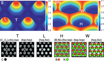
The atomic structure of graphene and boron nitride sp2 networks on transition metals is driven by coincidence or incommensurate lattices (see Figure 1) Land et al. (1992); N’Diaye et al. (2006); Marchini et al. (2007); Pan et al. (2007); de Parga et al. (2008); Paffett et al. (1990); Corso et al. (2004); Morscher et al. (2006); Preobrajenski et al. (2007).
For -BN/Rh(111) BN units coincide with Rh units Corso et al. (2004); Bunk et al. (2007) and similar lattice constants have been observed for adsorbed graphene systems de Parga et al. (2008); Marchini et al. (2007); N’Diaye et al. (2006). The concomitant variation of the local coordination of the substrate and the adsorbate atoms divides the unit cells into regions with different lateral coordination. The notation (B,N)(top,hcp) refers to the local configuration, where a B atom sits on top of the Ru atom in the first substrate layer and N on top of the hexagonal close packed (hcp) site, i.e. on top of the Ru atom in the second layer. Therefore 3 regions (fcc,top), (top,hcp) and (hcp,fcc) can be distinguished (see Figure 1). Whereas BN has a base with two different atoms in the unit cell, the base of graphene consists of two identical carbon atoms C and C which become distinguishable by the local coordination to the substrate. The local coordination of the (B,N) or (C,C) units in the honeycomb overlayer gradually shifts along the diagonal of the unit cell from (hcp,fcc) via (fcc,top) and (top,hcp) back to (hcp,fcc). In g/Ru the local (fcc,top) and (top,hcp) coordination leads to close contact between the (C,C) atoms and the substrate Wang et al. (2008) while (B,N) is strongly interacting only in the (fcc,top) coordination Laskowski and Blaha (2008). As a result, twice as many atoms are bound in strongly interacting regions in g/Ru when compared to -BN/Ru. In the following we call the tightly bound region -region and the loosely bound [(C,C)(hcp,fcc)] -region. This causes the most obvious difference in the atomic structure of the two sp2 networks.
The single layer graphene has been grown in ultrahigh-vacuum by thermal decomposition of () ethene (C2H4) on the hot Ru(0001) surface which had been cleaned by standard procedures. It was characterized with scanning tunneling microscopy and low energy electron diffraction.
Ab initio calculations are performed with the VASP package based on DFT, which implements PAW pseudopotentials Kresse and Joubert (1999) and the PBE exchange correlation functional in the Generalized Gradient Approximation (GGA) Perdew et al. (1996). For the band structure calculations epitaxial () C or BN/Ru structures are investigated with the lattice constant of graphene, a 4-layer Ru slab, a -sampling and cutoff. For the calculation of the atomic structure and the electrostatic potential, large moiré periodicities are considered with asymmetric (structure) and symmetric (potential) slabs.
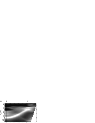
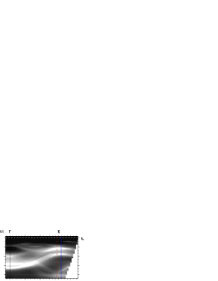
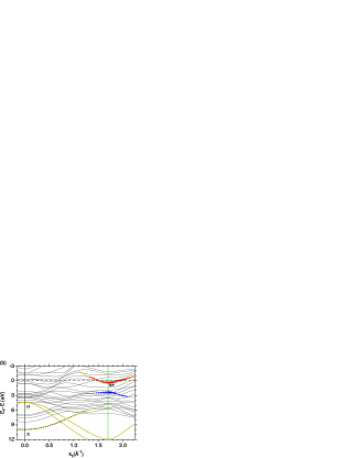
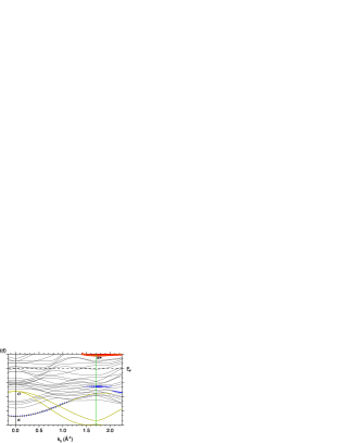
The hybridization of the carbon pz orbitals with the substrate atoms breaks the symmetry between the C and the C atoms. This is reflected in the band structure where a large -band gap opens at . Figure 2(a) shows the measured band structure for g/Ru(0001) along . At the -band levels off at a binding energy of . This strong hybridization is in line with observations on g/Ni(111) Nagashima et al. (1995). The experiment is in good agreement with calculations for a () graphene sheet above the topmost Ru layer with (C,C)(top,hcp) (Figure 2(b)). Figure 2(c) shows the same section of -space for -BN/Ru(0001). The -band levels off at a binding energy of . Also -BN on Ru is well described with calculations for a () (B,N)(fcc,top) sheet above the topmost Ru layer (Figure 2(d)). Theory also shows that the two atoms in the base of the sp2 networks have a different weight on the different bands. For the case of BN the -band is mainly nitrogen derived, while the unoccupied -band has its main weight on the boron atoms. For the () model of graphene only the C atom contributes to the -band while the -band has equal portions from top and hollow site atoms. The effect of C-Ru hybridization is reflected by localized states in the -bandgap that are mainly C-Ru derived. A distinct difference between graphene and -BN nanomesh is the -band splitting of for the BN bands that belong to the ‘wires’ and the ‘holes’ respectively Goriachko et al. (2007). The band splitting of -BN was assigned to the dielectric nature of -BN and the workfunction difference between the ‘hole’ and the ‘wire’ regions. For graphene no splitting is observed, where a splitting smaller than could not be resolved by the experiment. This can be explained by a smaller corrugation of the graphene layer or by the metallic nature of graphene.
The metallicity of g/Ru(0001) is reflected in the measured Fermi surface map (FSM) which is compared to that of -BN/Ru(0001) in Figure 3.


The FSM of -BN/Ru(0001) shows only bands that are also seen on the bare Ru(0001) surface. On the other hand, g/Ru(0001) displays states at the Fermi level that are reminiscent to the Dirac points at the points of free standing graphene Bostwick et al. (2007). The bandstructure measurements in Figure 2(a) demonstrate that these graphene related states are part of the -band, which means that charge is transferred from the substrate to the graphene. The Luttinger volume of the electron pockets near corresponds to the number of transferred electrons , where is taken as the full width at half maximum of the intensity on an azimuthal cut across , in radians (Figure 3(c)). For the FSM in Figure 3(a) we find , which translates to electrons per graphene unit cell. Of course, this value is the average for the whole graphene unit cell.
The differences in the atomic and electronic structure are also reflected in the potential energy surfaces that drive the functionality of the super structures as templates for the formation of molecular arrays. In Figure 4(a) the calculated electrostatic potential for g/Ru(0001) above the carbon atoms is shown.
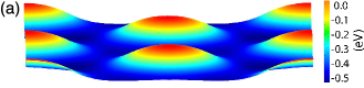


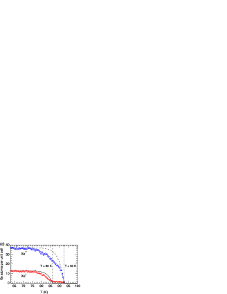
As for the case of -BN/Rh(111) nanomesh the energy corrugation correlates with the atomic corrugation Dil et al. (2008). This potential is measured with photoemission of adsorbed xenon Wandelt (1984). Also for g/Ru(0001) two Xe bonding regions can be distinguished with distinct Xe 5p1/2 photoemission binding energies and spectral weight (Figure 4(b)). Assuming a Xe van der Waals radius of , 50 Xe atoms per g/Ru(0001) unit cell are expected for the monolayer coverage Martoccia et al. (2008). From the spectral weight and the known atomic structure it can be deduced that the XeT species on the tightly bonded graphene has the higher Xe 5p1/2 photoemission binding energy and contains 37 atoms at full coverage. The XeL species with lower photoemission binding energy corresponds to Xe adsorbed on the loosely bonded graphene. The binding energy difference between these two species of is determined from a fit of two Gaussians with equal width and does not depend on the coverage. This value reflects a local work function difference between - and -graphene and is in agreement with the theoretical result shown in Figure 4(a). Like on the -BN nanomesh the tightly bonded regions have a lower work function. However, for g/Ru(0001) the local work function difference is about lower than for the case of -BN/Rh(111). Intuitively, this is related to the metallic nature of the graphene that screens out lateral electric fields in the graphene. The better screening of graphene is indeed reflected in the Xe 5p1/2 final state binding energy as referred to the vacuum level Kaindl et al. (1980). Table 1 shows that of XeT on g/Ru(0001) is 210 meV smaller than that of XeH on -BN/Rh(111).
From the thermal desorption the Xe adsorption energy is inferred. In Figure 4(d) the spectral weights of the Xe species are shown as a function of temperature (heating rate ). The temperatures at which the two Xe species disappear indicate that XeT is about stronger bound than XeL. In order to compare g/Ru with -BN/Rh Dil et al. (2008), the temperature dependent weights of the two Xe species were fitted to zero order desorption. From the desorption energies are found (see Table 1).
| -BN/Rh(111) | g/Ru(0001) | ||||
|---|---|---|---|---|---|
| Phase | XeL | XeT | |||
| 25 | 17 | 12 | 13 | 37 | |
The values are slightly smaller than the desorption energies on graphite ( Ulbricht et al. (2006)) and higher with respect to -BN/Rh. The fits for zero order desorption show that the XeT species are not well described with a single desorption energy (dashed line in Figure 4(d)). In the -BN/Rh case two XeH phases (CH and RH) had been identified by a pronounced kink in the desorption spectrum of XeH. The more strongly bound of these two phases was assigned to XeH atoms at the rims of the holes where dipole rings induce an enhanced polarization and bonding. For g/Ru(0001) a clear kink is not visible, but the deviations from the fit also indicate variations in bonding strength of the XeT atoms. The difference to -BN/Rh may be understood by the different shape of the potential energy surface. If one nevertheless fits two XeT phases binding energies of and are obtained for g/Ru(0001). The small difference of is not unreasonable considering the lower work function modulation than for -BN/Rh.
In conclusion, the presented findings suggest that g/Ru is not a nanomesh, i.e. a corrugated single layer dielectric, but a corrugated single layer metal. However, it is also expected to act as a template for molecular trapping, where the metallicity of graphene imposes a stronger electronic coupling of adsorbates to the underlying transition metal.
Fruitful discussions with Peter Blaha and technical support by Martin Klöckner are gratefully acknowledged. We thank the Swiss National Science Foundation and the German Research Foundation for their financial support. M.L.B thanks the Humboldt foundation for a research fellowship. Part of this work was performed at the Swiss Light Source.
References
- Novoselov et al. (2004) K. S. Novoselov, A. K. Geim, S. V. Morozov, D. Jiang, Y. Zhang, S. V. Dubonos, I. V. Grigorieva, and A. A. Firsov, Science 306, 666 (2004).
- Corso et al. (2004) M. Corso, W. Auwärter, M. Muntwiler, A. Tamai, T. Greber, and J. Osterwalder, Science 303, 217 (2004).
- Marchini et al. (2007) S. Marchini, S. Günther, and J. Wintterlin, Physical Review B 76, 075429 (2007).
- Pan et al. (2007) Y. Pan, D. X. Shi, and H. J. Gao, Chinese Physics 16, 3151 (2007).
- de Parga et al. (2008) A. L. V. de Parga, F. Calleja, B. Borca, M. C. G. Passeggi, J. J. Hinarejos, F. Guinea, and R. Miranda, Physical Review Letters 100, 056807 (2008).
- Goriachko et al. (2007) A. Goriachko, Y. B. He, M. Knapp, H. Over, M. Corso, T. Brugger, S. Berner, J. Osterwalder, and T. Greber, Langmuir 23, 2928 (2007).
- Berner et al. (2007) S. Berner, M. Corso, R. Widmer, O. Groening, R. Laskowski, P. Blaha, K. Schwarz, A. Goriachko, H. Over, S. Gsell, et al., Angewandte Chemie-International Edition 46, 5115 (2007).
- Dil et al. (2008) H. Dil, J. Lobo-Checa, R. Laskowski, P. Blaha, S. Berner, J. Osterwalder, and T. Greber, Science 319, 1824 (2008).
- Land et al. (1992) T. A. Land, T. Michely, R. J. Behm, J. C. Hemminger, and G. Comsa, Surface Science 264, 261 (1992).
- N’Diaye et al. (2006) A. T. N’Diaye, S. Bleikamp, P. J. Feibelman, and T. Michely, Physical Review Letters 97, 215501 (2006).
- Paffett et al. (1990) M. T. Paffett, R. J. Simonson, P. Papin, and R. T. Paine, Surface Science 232, 286 (1990).
- Morscher et al. (2006) M. Morscher, M. Corso, T. Greber, and J. Osterwalder, Surface Science 600, 3280 (2006).
- Preobrajenski et al. (2007) A. B. Preobrajenski, A. S. Vinogradov, M. L. Ng, E. Cavar, R. Westerstrom, A. Mikkelsen, E. Lundgren, and N. Mårtensson, Physical Review B 75, 245412 (2007).
- Bunk et al. (2007) O. Bunk, M. Corso, D. Martoccia, R. Herger, P. R. Willmott, B. D. Patterson, J. Osterwalder, I. van der Veen, and T. Greber, Surface Science 601, L7 (2007).
- Wang et al. (2008) B. Wang, M. L. Bocquet, S. Marchini, S. Günther, and J. Wintterlin, Physical Chemistry Chemical Physics 10, 3530 (2008).
- Laskowski and Blaha (2008) R. Laskowski and P. Blaha, Journal of Physics-Condensed Matter 20, 064207 (2008).
- Kresse and Joubert (1999) G. Kresse and D. Joubert, Physical Review B 59, 1758 (1999).
- Perdew et al. (1996) J. P. Perdew, K. Burke, and M. Ernzerhof, Physical Review Letters 77, 3865 (1996).
- Nagashima et al. (1995) A. Nagashima, N. Tejima, Y. Gamou, T. Kawai, and C. Oshima, Physical Review B 51, 4606 (1995).
- Bostwick et al. (2007) A. Bostwick, T. Ohta, T. Seyller, K. Horn, and E. Rotenberg, Nature Physics 3, 36 (2007).
- Wandelt (1984) K. Wandelt, Journal of Vacuum Science & Technology A: Vacuum, Surfaces, and Films 2, 802 (1984).
- Martoccia et al. (2008) D. Martoccia, et al., Physical Review Letters (2008), submitted.
- Kaindl et al. (1980) G. Kaindl, T. C. Chiang, D. E. Eastman, and F. J. Himpsel, Physical Review Letters 45, 1808 (1980).
- Ulbricht et al. (2006) H. Ulbricht, R. Zacharia, N. Cindir, and T. Hertel, Carbon 44, 2931 (2006).