High-Frequency Properties of a Graphene Nanoribbon Field-Effect Transistor
Abstract
We propose an analytical device model for a graphene nanoribbon field-effect transistor (GNR-FET). The GNR-FET under consideration is based on a heterostructure which consists of an array of nanoribbons clad between the highly conducting substrate (the back gate) and the top gate controlling the dc and ac source-drain currents. Using the model developed, we derive explicit analytical formulas for the GNR-FET transconductance as a function of the signal frequency, collision frequency of electrons, and the top gate length. The transition from the ballistic and to strongly collisional electron transport is considered.
pacs:
73.50.Pz, 73.63.-b, 81.05.UwI Introduction
The utilization of the patterned graphene which constitutes an array of sufficiently narrow graphene nanoribbons as the basis for field-effect transistors (GNR-FETs) opens up wide opportunities for the energy band engineering promoting the achievement of the optimal device parameters. By properly choosing the width of the nanoribbons, one can fabricate the graphene structures with relatively wide band gap but rather high electron (hole) mobility 1 ; 2 (see also Refs. 3 ; 4 ; 5 ; 6 ; 7 and the references therein).
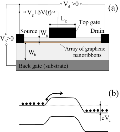
In this paper, we present an analytical device model for a graphene-nanoribbon FET (GNR-FET) and obtain the device characteristics. The GNR-FET under consideration is based on a patterned graphene layer which constitutes a dense array of parallel nanoribbons of width with the spacing between the nanoribbons . The nanoribbon edges are connected to the conducting pads serving as the transistor source and drain. A highly conducting substrate plays the role of the back gate, whereas the top gate serves to control the source-drain current. The device structure is schematically shown in Fig. 1. Using the developed model, we calculate the potential distributions in the GNR-FET as a function of the back gate, top gate, and drain voltages, , , and (reckoned from the potential of the source contact), respectively, and the GNR-FET dc characteristics. This corresponds to a GNR-FET in the common-source circuit. The case of common drain will briefly be discussed as well. For the sake of definiteness, the back gate voltage and the top gate voltage are assumed to be, respectively, positive and negative ( and ) with respect to the potential of the source contact, so we consider GNR-FETs with the channel of n-type.
The paper is organized as follows. In Sec. II, the GNR-FET device model is considered. Here the main equations governing the GNR-FET operation are presented. Section III deals with the derivation of the GNR-FET steady-state characteristics. The results of this section generalize those obtained previously 7 for the case of ballistic electron transport for arbitrary values of the electron collision frequency. In Sec. IV, we derive a general formula for the ac source-drain current as a function of the signal frequency and the device material and structural parameters. Section V is devoted to the analysis of the GNR-FET transconductance in a wide range of the signal frequencies and device parameters. Section VI deals with the interpretation of the obtained characteristics and discussion of their limitations. In Sec. VII, we draw the main results.
II GNR-FET model
We consider a GNR-FET with the structure shown in Fig. 1(a). The back gate and drain voltages and (with ) are positive. As a result, the electron densities in the channel sections adjacent to the sourse and drain (not covered by the top gate) are, respectively, given by 7
| (1) |
where is the dielectric constant, is the thickness of the layer between the GNR array and the back gate. The top gate voltage comprises the dc and ac components, and , respectively (). When the absolute value of the dc component of the top gate voltage is sufficiently large (), the channel section beneath the top gate is essentially depleted and potential barriers for the electrons incident from the source and drain sections of the channel are formed (see Fig. 1(b)). In the case of a GNR-FET with sufficiently long top gate (), the height of the barriers can be presented as 7
| (2) |
where and . As seen from Eq. (2), the variation of the top gate voltage leads to the variarion of the potential barrier heights and, consequetly, to the variation of the electron current above the barrier.
We assume that the electron energy spectrum of the lowest GNR subband can be presented as
| (3) |
Here the energy is reconed from the subband bottom, is the energy gap, is the momentum in along the nanoribbon, is the electron effective mass (near the subband bottom), and cm/s is the characteristic velocity of electrons in graphene (and in GNRs). The energy gap and the effective mass depend on the GNR widths . In the simplest model, . The electron transport in the section of the electron channel beneath the top gate (the gated section), in which the electron density is small, so that one can neglect the electron-electron scattering, can be described by the following kinetic equation for the electron distribution function:
| (4) |
Here
| (5) |
is the electron velocity with the momentum , is the collision frequency of electrons associated with the disorder (including edge roughnesses) and acoustic phonons. We disregard the inelasticity of the scattering on acoustic phonons, so that all the scattering mechanisms under consideration result in the change of the electron momentum from to . The probability of the electron elastic scattering is essentially determined by the density of state. Taking into account collisional broadening 8 ; 9 (see also, Refs. 10 ; 11 , we approximate the dependence in question as , where is the value of the collisional frequency of thermal electrons, chracterizes the collision broadening, and . If , , whereas at (but ), one obtains .
The bondary conditions for are set at the points in the electron channel beneath the edges of the top gate, i.e., at and :
| (6) |
Here
are the distribution functions of the electrons incoming to the channel section in question from the source and drain sides, respectively, is the Boltzmann constant, and is the temperature,
III Steady-State Characteristics
Solwing Eq. (4) with boundary conditions (6) at , for the dc component of the electron distribution function we obtain the following relationship:
| (7) |
Here . For definiteness, here and in the following we assume that the modulus of the top gate voltage is sufficiently large, so that the channel beneath this gate is essentially depleted 7 . At such top gate voltages, the GNR-FET dc transconductance is much larger that when is small.
The source-drain dc current can be calculated using the following formula:
| (8) |
Considering Eqs. (7) and (8), we obtain
| (9) |
As follows from Eq. (3),
| (10) |
Since the kinetic energy of electrons propagating in the gated section of the channel of realistic GNR-FETs can be assumed small in comparison with the energy gap (), from Eq. (11) one obtains the following simple relation: . Taking this into account, from Eq. (9) we obtain
| (11) |
Here
| (12) |
is the dc source-drain current in the ballistic regime 7 , and the factor
| (13) |
describes the effect of electron collisions. Here can be called the ballistic parameter This parameter can also be presented as , where is the characteristic electron transit time beneath the top gate and is the thermal electron velocity. The case corresponds to near ballistic transport of the majority of electrons (except, possibly, a fraction of low energy electrons). In the opposite case , the collisions substantially affect the electron transport. When tends to zero, turns to unity. Hence, in the ballistic regime of the electron transport through the section of the channel covered by the top gate, Eq. (11) yields , where the value as a function of the gate and drain voltages coincides with that obtained previously 7 . In the case of collision-dominated electron transport , from Eq. (13) we obtain
| (14) |
where is a coefficient (weakly dependent on ).
Equations (11) - (14) desribe the GNR-FET dc current-voltage characteristics, i.e., the dependences of the dc source-drain current on the gate voltages as well as the drain voltage, which generalize those derived previously 7 for the purely ballistic transport.
IV Small-signal analisis
Consider now the case when the top gate voltage comprises a small-signal comonent , where and are the signal amplitude and frequency. In such a case, Eq. (4) for the ac component of the distribution function in the channel section beneath the top gate reduces to the following:
| (15) |
As follows from Eq. (6), the bondary conditions for in the most practical case can be presented in the following form:
| (16) |
Solwing Eq. (15) with boundary conditions (16) and using Eq. (2), we arrive at the following formula:
| (17) |
where . Taking into account that the ac component of the electron current in the channel beneath the top gate is given by
| (18) |
and using Eq. (20), we obtain
| (19) |
In particular, near the drain-side edge of the top gate (), Eq. (19) yields
| (20) |
Equation (20) can be presented as
| (21) |
where
| (22) |
where is given by Eq. (12) and .
In this case, setting in Eq. (22), we obtain
| (23) |
Naturally, at , Eq. (23) yields .
V Transconductance
The electrons passing from the the channel section beneath the top gate into the drain section of the channel between the edge of the top gate () and the edge of the highly conducting regions adjucent to the drain contact (), induce the current through the latter. This induced source-drain terminal ac current can be calculated using the Shockley-Ramo theorem 12 ; 13 accounting for the features of the geometry of all highly conducting contacts 14 ; 15 . The terminal ac current is given by
| (24) |
Here is the length of the depleted region between the top gate and the drain (see Fig. 1) determined by the applied dc voltages. In particular, if , this depleted region extends to the drain contact. The electron drain transit-time factor can be calculated using the following formula:
| (25) |
where is the electron transit time across the gate-drain region, and is the form-factor accounting for the shape of the highly conducting regions (top gate and drain contact as well as the higly conducting portion of the channel near the latter contact). The electric field in the gate-drain region, so that their average velocity can substantially exceed the electron thermal velocity. Hence, one might expect that the electron transit time across the gate-drain region is sufficiently short . As a result, in the most interesting frequency range , one obtains . In this case, one can put . The transit-time effects which lead to a significant frequency dependence of and, in particular, to a marked decrease in at elevated frequencies are discussed in the following.
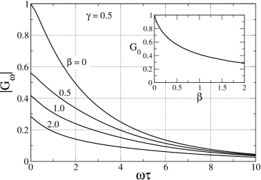
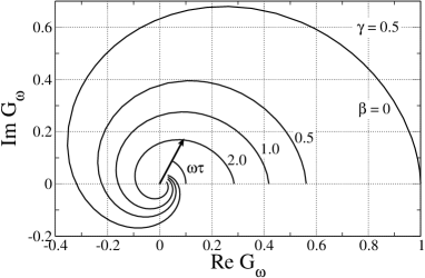
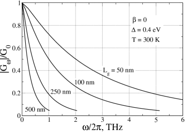
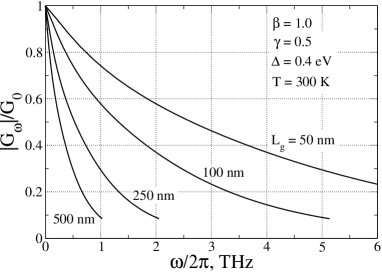
Figure 2 shows the frequency dependences of the GNR-FET transconductance modulus calculated for different values of the ballistic parameter . It was assumed that . The inset shows as a function of . As it was demonstrated the vs dependence is almost insensitive to variations of parameter ; the maximum deviation from the dependence shown in the inset in Fig. 2 was less than when varied from to 2. In this and the following figures, we set eV and K. Figure 3 demonstrates the amplitude-phase diagram calculated for the same parameters as in Fig. 2. The normalized transconductance as a function of the signal frequency calculated for GNR-FETs with different top gate lengths is show in Figs. 4 and 5.
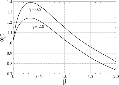
Figure 6 shows the dependence of the normalized theshold frequency at which . It is instructive that the obtained dependences exhibit maxima at certain values of the ballistic parameter (not at as one might expect). Moreover, the height of these maxima decreases with increasing parameter , which characterizes the collisional broadening (see Sec. II).

VI Discussion
The effect of the dependence of the threshold frequency on parameters and can be attributed to the following. First, at the ballistic electron transport, the frequency dependence of is actually determined not only by the characteristic transit time but also by the thermal spread in the electron velocities 16 ; 17 . The latter is about the thermal electron velocity . The scattering of electrons, particularly strongly dependent on the electron momentum, can influence the effective spead in velocities. Indeed, when , i.e., when the low-energy electrons (with small ) exhibit rather strong scattering, their contribution to the current decreases with simultanious decrease in the effective spead in velocities. This can be seen, in particular, from Eq. (7) in which the asymmetric part of the distribution function is . Since the term sharply increases when tends to zero, this function can be fairly small in the range of small (especially at small ), while at large it tends to the Maxwellian function. This implies that, the momentun distribution can shrink and the velocity spread can decrease due to specific feature of the electron scattering in GNRs. A significant increase in the threshold frequency can be achieved if the directional electron velocity markedly exceeds the thermal velocity. This can occur in GNR-FETs with the GNRs with varied widths (increasing from the source-side edge of the top gate to its drain-side) and the pertinent decrease in the energy gap. In such hetero-GNRs, the electrons can accelerate propagating from the source to drain (see, for instance, Ref. 18 ).
As was mentioned above, factor associated with the electron transit-time effects in the region between the top gate and drain contact depends on the transit angle and the form-factor . Figure 7 shows the frequency dependence of for the following two cases: (a) and (b) 14 ; 15 . The form-factor (a) can be attributed to the case when the drain contact is rather bulk, so that the source-drain ac current is induced primarily in this contact (not in the highly conducting portion of the channel adjacent to the drain contact). The form-factor (b) corresponds to the case when the ac current is induced mostly in the highly conducting region or when the drain contact is a blade-like. Both such cases can take place depending on the spacing, , between the top gate and the drain contact and the bias voltages and . At , the region of the channel between the top gate and the drain contact is virtually depleted. Hence, if the drain contact is bulk, with . The frequency dependences of calculated for the cases under consideration are shown in Fig. 7. As seen from Fig. 7, markedly drops with increasing transit angle when the latter exceeds unity. This effect is not important if the frequency-dependent GNR-FET transconductance is mainly limited by the electron delay under the top gate, i.e., if . However, at , the net transconductance is determined by the product of and corresponding to curves shown in Fig. 4 and Fig. 7, respectively.
VII Conclusions
(1) We proposed an analytical device model for a GNR-FET based on a heterostructure which consists of an array of nanoribbons clad between the highly conducting substrate (the back gate) and the top gate.
(2) Using this model, we derived explicit analytical formulas for the GNR-FET transconductance as a function of the signal frequency in wide ranges of the collision frequency of electrons and the top gate length.
(3) The variation of the GNR-FET high-frequency characteristics due to the transition from the ballistic and to strongly collisional electron transport was traced. It was shown that the threshold frequency can nonmonotonically depend on the ballsitic parameter.
VIII Acknowledgment
The work was supported by CREST the Japan Science and Technology Agency, CREST, Japan.
References
- (1) B. Obradovic, R. Kotlyar, F. Heinz, P. Matagne, T. Rakshit, M. D. Giles, M. A. Stettler, and D. E. Nikonov, Appl. Phys. Lett. 88, 142102 (2006).
- (2) Z. Chen, Y.-M. Lin, M. J. Rooks, and P. Avouris, Physica E 40, 228 (2007).
- (3) K. Wakabayshi, Y. Takane, and M. Sigrist, Phys. Rev. Lett. 99, 036601 (2007).
- (4) Y. Quyang, Y. Yoon, J. K. Fodor, J. Guo, Appl. Phys. Lett. 89, 203107 (2006).
- (5) G. Liang, N. Neophytou, D. E. Nikonov, and M. S. Lundstrom, IEEE Tran. Electron Devices 54, 677 (2007).
- (6) G. Fiori and G. Iannaccone, IEEE Electron Device Lett. 28, 760 (2007).
- (7) V. Ryzhii, M. Ryzhii, A. Satou, and T. Otsuji, J. Appl. Phys. 103, 094510 (2008).
- (8) S. Briggs and J. P. Leburton, Phys. Rev. B 38, 8163 (1988).
- (9) S. Briggs, B. A. Mason, and J. P. Leburton, Phys. Rec. B 40, 12001 (1989).
- (10) G. Pennington and N. Goldsman, Phys. Rev. B 68 045426 (2003)
- (11) J. Guo and M. Lundstrom, Appl. Phys. Lett. 86, 133103 (2005)
- (12) W. Shockley, J. Appl. Phys. 9, 635 (1938)
- (13) S. Ramo, Proc. IRE 27, 584 (1939).
- (14) V. Ryzhii and G. Khrenov, IEEE Trans. Electron Devices 42, 166 (1995).
- (15) V. Ryzhii, A. Satou, M. Ryzhii, T. Otsuji, and M. S. Shur, J. Phys. Cond. Mat. (in press).
- (16) V. I. Ryzhii, V. A. Fedirko, and I. I. Khmyrova, Sov. Phys. Semicond. 18, 527 (1984).
- (17) V. I. Ryzhii, N. A. Bannov, and V. A. Fedirko, Sov. Phys. Semicond. 18, 481 (1984).
- (18) V. I. Ryzhii and V. A. Fedirko, Sov. Phys. Semicond. 18, 691 (1984).
- (19) M. Shur, Physics of Semiconductor Devices (Prentice Hall, New Jersey, 1990).
- (20) S. M. Sze, Physics of Semiconductor Devices (Wiley, New York, 1981).