Medium-Energy Ion Scattering study of strained holmium silicide nanoislands grown on silicon (100)
Abstract
We have used medium-energy ion scattering (MEIS) to quantitatively analyse the structure of holmium silicide islands grown on the Si(100) surface. Structure fitting to the experimental data unambiguously shows that the tetragonal silicide phase is present and not the hexagonal phase which is associated with the growth of nanowires at submonolayer coverages. Islands formed with a lower holmium coverage of 3 ML are also shown to be tetragonal which suggests that the hexagonal structure is not a low coverage precursor to the growth of the tetragonal phase. MEIS simulations of large nanoislands which include the effects of lateral strain relief have been performed and these compare well with the experimental data.
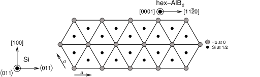
Whilst there have been many studies of rare-earth (RE) silicides on the Si(111) surface, relatively little was known about the growth mechanisms on the Si(100) surface until the discovery of self-assembled nanowires by Preinesberger et al. Preinesberger et al. (1998) These novel structures form when a suitable RE metal, eg. Gd, Kirakosian et al. (2002); McChesney et al. (2002); Chen et al. (2002a); Lee and Kim (2003); Liu and Nogami (2003a) Sc, Chen et al. (2002a) Dy, Preinesberger et al. (1998); Chen et al. (2003); Nogami et al. (2001); Liu and Nogami (2001, 2003b) Sm, Chen et al. (2002a) Er, Chen et al. (2003); Nogami et al. (2001); Chen et al. (2000, 2002b); Cai and Zhou (2004) Ho Nogami et al. (2001); Ohbuchi and Nogami (2002) or Y, Katkov and Nogami (2002) is deposited onto a clean Si(100) substrate held at an elevated temperature. Characteristic ‘wires’ measuring up to a micrometre in length, and typically only a few nanometres wide were observed by scanning tunneling microscopy (STM). This discovery and the potential technological applications of such conducting nanowires has motivated considerable interest over the last ten years Frangis et al. (1996, 1997); Chen et al. (1998, 2000); Nogami et al. (2001); Liu and Nogami (2001); Chen et al. (2002b); Ohbuchi and Nogami (2002); Chen et al. (2002c); Kirakosian et al. (2002); McChesney et al. (2002); Katkov and Nogami (2002); Chen et al. (2002a); Chi et al. (2003); Liu and Nogami (2003a, b); Lee and Kim (2003); Chen et al. (2003); Kuzmin et al. (2004); Cai and Zhou (2004); He et al. (2004); Harrison and Boland (2005); Pető et al. (2005); Tsai et al. (2005); Pasquali and Nannarone (2005); Ye et al. (2006a, b). Chen et al. have demonstrated that the growth of nanowires with extremely high aspect ratios is the result of the anisotropic lattice mismatch that results from the growth of the hexagonal, defect-AlB2 RE silicide on the Si(100) surface (see Fig. 1) Chen et al. (2000).
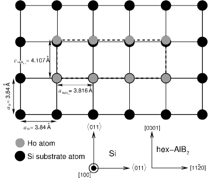
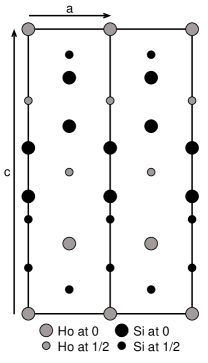
Depositing more RE metal causes islands to form with the surface displaying a periodicity. The structure of these RE silicide islands has been proposed to be either hexagonal, tetragonal (ThSi2) or orthorhombic (GdSi2) Preinesberger et al. (1998); Frangis et al. (1996, 1997); Chen et al. (2002b); Liu and Nogami (2003b, a); Cai and Zhou (2004); He et al. (2004); Ye et al. (2006a, b). All three of these phases are known to exist in the bulk and their lattice constants have been measured and it is known that the bulk orthorhombic phase is only a small distortion of the tetragonal phase Maex and Rossum (1995). A side-view schematic of the ThSi2 structure is shown in Fig. 2. Evidence for the growth of the tetragonal form has generally been inferred from lattice mismatch arguments, along with STM measurements of step heights in the silicides on the Si(100) surface Cai and Zhou (2004). SXRD measurements also yield information which appears to confirm that Er silicide islands adopt the tetragonal form, with the surface periodicity interpreted as being due to Si adatoms Chen et al. (2002b).
STM experiments reveal that the island morphology is very sensitive to the RE metal deposited and to the annealing temperature used. Those RE metals (Nd, Sm, Yb) that have a low anisotropy in their lattice match to the substrate form compact 3D islands Nogami et al. (2001). Those that have a high anisotropy form both elongated and compact islands, depending upon the growth temperature. Growth at lower temperatures (600∘C) causes the formation of elongated islands and growth at temperatures above 650∘C results in compact 3D islands. However, the two island morphoplogies have been observed to coexist, especially when using intermediate annealing conditions.
Dysprosium silicide provides an interesting case study. The elongated islands have typical dimensions 2 nm high, 15 nm wide, and 500 nm long and the smaller compact islands have typical dimensions 5 nm high, 50 nm wide and 200nm long He et al. (2004). Using high resolution cross-sectional TEM, Ye et al. demonstrated that elongated and non-elongated islands coexist when Dy silicide is grown at 600 ∘C 650 ∘C on the Si(100) surface Ye et al. (2006a). They proposed that the structure of the elongated islands was hexagonal, and the excessive stress within this structure (due to the large -axis mismatch) is relieved through dislocations and tilting across the width of the island. The non-elongated islands were found to be a tetragonal or orthorhombic structure with only a small amount of tilting required to relieve the stress, since the lattice match is relatively small in both directions. It was also noted that there was some expansion of the -axis to relieve the stress in much the same way as has been demonstrated for the 2D and 3D RE silicides on Si(111) Bonet et al. (2005); Wood et al. (2006). However, the recent HR-TEM study by He et al. claims that the compact 3D Dy silicide islands are in fact a fully relaxed, and hence stress free, hexagonal form, whilst the elongated nanowire islands are tetragonal/orthorhombic, with the faulted stacking relieving the stress in the structure He et al. (2004). The delicate energy balance within the silicide in this particular example is also highlighted by the fact that there is both a tetragonal and an orthorhombic phase of Dy silicide in the bulk.
Despite the many studies that have been conducted, it has been noted in recent work that no ideal crystallographic determination has been possible to clearly prove once and for all the true nature of the 3D islands Pasquali and Nannarone (2005); He et al. (2004); Ye et al. (2006b) created when the rare earth metals form a silicide in this way. MEIS is of particular value in the study of these nanostructures since the large mass contrast of Ho and Si allows the elucidation of the silicide structure free from substrate effects. This also means that the technique is able to isolate the regions of interest on the surface by only selecting the Ho signal for the structural optimisation.
I EXPERIMENT
All MEIS data were obtained at the UK MEIS facility at STFC Daresbury Laboratory. The experiments were conducted under ultra-high vacuum (UHV), with typical base pressures of mbar. Clean Si(100) samples (cut from a lightly doped n-type wafer) were prepared by e-beam heating to ∘C for 1 min, then slowly cooled ( 100 ∘C min-1) between 1000 ∘C and 600 ∘C to ensure an ordered surface was obtained. Temperature measurements were made using an infrared pyrometer. The heating cycles were repeated until a sharp low-energy electron diffraction (LEED) pattern was observed. The 3D silicide islands were then formed by depositing approximately 6 ML of Ho from a quartz crystal calibrated tantalum boat source onto this clean Si(100) surface, which was held at ∘C during deposition and for 5 min afterwards. When a LEED pattern was observed and the Auger electron spectrum showed the samples to be free from contamination, they were transferred under UHV into the ion scattering chamber.
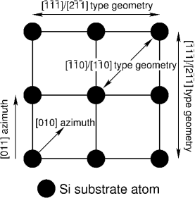
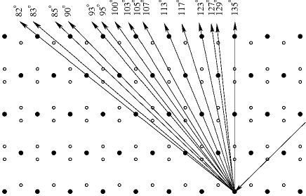
The ion scattering data were taken using 100 keV H+ ions incident upon the sample and the scattered ions were detected using an angle-resolving toroidal-sector electrostatic ion-energy analyser and its microchannel plate detector. The MEIS spectra confirmed that the samples were free of contaminants and data were acquired with a total dose of ions cm-2. Further details about the Daresbury MEIS facility can be found in the literature Spence et al. (2000a, 2002, b); Bonet et al. (2005); Wood et al. (2005). During each experiment two different incident beam directions onto the sample were used. These beam directions are shown with respect to the substrate in fig. 3. The notation for each geometry defines the ingoing crystal direction and an outgoing crystal direction that lies in the detected angular range of the scattered ions.
II STRUCTURE FITTING: TETRAGONAL OR HEXAGONAL?
Due to the contention in the literature regarding whether these islands take the hexagonal, tetragonal or orthorhombic form, MEIS proves particularly powerful since it can clearly demonstrate the presence of one of these structures. In this work we have used the XVegas code Frenken et al. (1986) which uses Monte-Carlo methods to simulate the blocking curves of a proposed structural model.
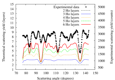
Fig. 4 shows the simulated blocking curves obtained when differing numbers of layers of RE are present in the hexagonal structure for the / geometry. The interlayer separation of all the Ho layers has been optimised to give the best visual agreement with experimental data, with the two intermediate Si layers lying 1/3 and 2/3 of this layer separation from the Ho layer beneath. A Ho–Ho layer separation of 3.28 Å has been found to give the best-fit. However, the quality of the fits obtained is very poor, clearly demonstrating that this is not the correct structure. To make this clearer, the fit for 6 layers of Ho is shown in Fig. 4. At scattering angles of 88, 90, 100, 106, 118, 127 and 142 there are major discrepancies between the experimental data and the best-fit simulations. The fully relaxed hexagonal structure that was proposed by He et al. He et al. (2004) does not explain the experimental blocking curves either, as such a structure would produce almost identical blocking curves, but would yield a smaller -axis of the silicide.
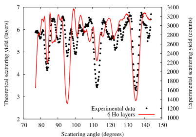
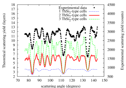
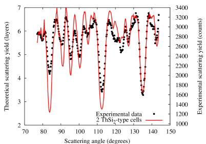
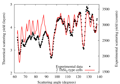
The tetragonal structure has also been fitted to the data, since it is assumed that the silicide takes the same and values as the Si substrate to form an epitaxial overlayer. This goes against the available data in the literature regarding the structure of the bulk Ho silicides, as no tetragonal phase has been observed (though the orthorhombic GdSi2 form has been reported with lattice parameters of = 4.03 Å, = 3.944 Å and = 13.30 Å) Maex and Rossum (1995). Conducting simulations of such a tetragonal structure gives the fits for the / geometry shown in Fig. 5, which are for structures that are one, two and three ThSi2-type cells in height. It is clear that a crystal with a depth of two ThSi2 cells produces the best match. The detailed structure fits are shown in figures 5 and 5. The r.m.s. thermal vibrations of the Ho atoms were set to the bulk metal value of 0.13 Å, whilst a fitting of the Si vibrations gives an enhanced value of 0.15 Å. These vibrations are consistent with the previous MEIS studies of 2D and 3D RE silicides on Si(111) Wood et al. (2005, 2006), with the factor of two enhancement for the Si atoms possibly indicating the presence of static disorder in these layers. This could be due to the presence of Si vacancies Chi et al. (2003); Tsai et al. (2005).
III AN ANOMALOUS C-AXIS VALUE
The assumption that the silicide grows epitaxially on the Si(100) surface yields a constant -axis value throughout this silicide (13.14 Å) that is much smaller than the value of 13.30 Å for the bulk silicide. We would expect that the stress induced through a contraction of the Ho silicide - and -axes at the interface, would be released through an expansion in the perpendicular direction and such behaviour has been directly observed in other rare earth silicide surfaces Bonet et al. (2005); Wood et al. (2006). In particular, Ye et al. have reported an expansion in the -axis of the silicide relative to the bulk value for Dy on Si(100) Ye et al. (2006a).
One explanation of this observation could be that the silicide is incommensurate with the Si substrate. Hence it would seem reasonable to assume that the silicide takes the orthorhombic form that is observed for bulk Ho silicide. Refitting the experimental data to simulations of this structure, where = 4.030 Å and = 3.944 Å, yields almost identical fits, but with a -axis of 13.70 Å. This large value of the silicide -axis does not make sense according to the established trend in strain either, as it would be expected that the lack of strain at the interface would not cause any expansion in the -axis of the silicide relative to the bulk value. Thus it can be concluded that it is not the bulk form of the silicide that is present on the surface; it must be some intermediate form.
One of the limitations of MEIS when only using the Ho blocking curves to solve crystallographic structure is that it is not possible to exclusively determine both the - and -axis lattice constants of the silicide. This is because any difference in the silicide -axis could be compensated by a change in the -axis to produce blocking curves with blocking dips in the same positions. Hence, a particular ratio will yield a series of blocking curves that are exactly the same, even though the actual lattice parameters may be very different. We have performed a series of simulations, each with a fixed -axis, in which the -axis has been optimised by varying the layer separation of a silicide that is two ThSi2 cells in height. These results are shown in Table 1.
| (Å) | ( 0.04 Å) | ( 0.04 Å) | ( 0.04 Å) | |||
|---|---|---|---|---|---|---|
| 3.84 | 13.12 | 13.16 | 13.14 | |||
| 3.88 | 13.24 | 13.28 | 13.26 | |||
| 3.92 | 13.40 | 13.44 | 13.42 | |||
| 3.96 | 13.52 | 13.56 | 13.54 | |||
| 4.00 | 13.68 | 13.72 | 13.70 |
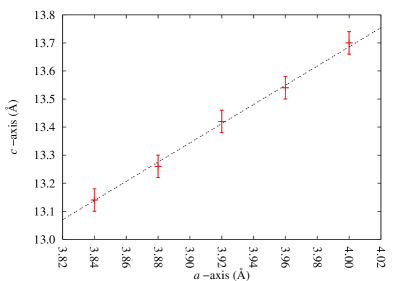
The data from Table 1 are plotted in Fig. 6 and the straight line fit defines a ratio of 3.42 0.01. The positive gradient suggests that as the lateral lattice constant of the tetragonal unit cell is reduced to match that of the substrate, the lattice constant perpendicular to the surface also contracts and this is true for all pairs of , values. As noted earlier, we might expect the opposite to occur and the -axis to expand in order to maintain the volume of the unit cell.
IV SIMULATION OF STRAINED ISLANDS
There is another reason that might explain the unusually low -axis suggested by the fitting procedure. If the lateral lattice constant of the unit cell is constrained to match that of the substrate at the interface and is allowed to expand to relieve strain as we move away from the interface then the blocking angles will be shifted. The average -axis throughout the structure will increase and so will the fitted -axis in order to maintain the ratio of 3.42. This effect would allow for interfacial matching and would at the same time provide a more physically meaningful thickness for the silicide.
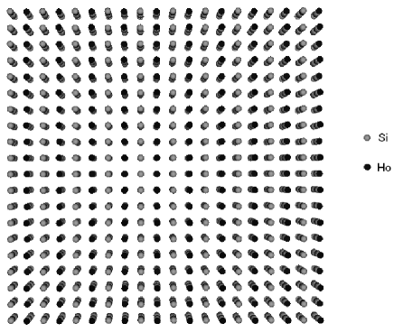
Simulation of this effect is computationally intensive. Unit cells with lateral strain as a function of height do not laterally tesselate ad-infinitum and a structure with finite lateral extent must be considered. This must be large enough to approach the size of a typical surface island but small enough to be computationally tractable. We have taken a unit cell with a 1010 lateral extent, making an island 38.438.4 Å2. This is two tetragonal unit cells deep and in total includes 2500 atoms. Computational resources prohibit us from a full optimisation of the strained structure in terms of interlayer spacings or vibrational amplitudes. Instead we have taken values suggested from the structure fitting carried out on the 112 cells detailed earlier in this work. The lateral lattice constants are allowed to relax from a value of 3.84 Å at the bottom of the supercell (interfacial matching to Si(100)) to 3.99 Å at the top of the supercell (the averaged unstrained lateral lattice constant of bulk orthorhombic holmium silicide). The strain relief is just a linear function of height and, for example, we have not considered a case in which only the few layers near the interface are significantly strained. The strained island is shown from above in Fig. 7.
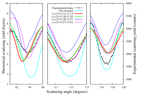
Since we cannot currently fully optimise the -axis in such a strained island we have simulated the blocking curves for four such islands, each with a different depth. This depth is varied by choosing two different -axes for the two unit cells that form the island. These four -axis values are; 1) both as bulk -axis values (13.30 Å), 2) both at the values obtained earlier in structure fitting with 112 cells with no strain relief (13.14 Å), 3) expansion of the -axis of the cell nearest the interface by 2% and a bulk -axis value in the top unit cell (13.57 Å, 13.30 Å) and 4) expansion of the -axis of the cell nearest the interface by 4% and the top cell by 2% (13.83 Å, 13.57 Å). The calculated blocking curves are shown in Fig. 8 for the / geometry, the / geometry not being calculated because it would require averaging over two possible domains and thus twice as many simulations.
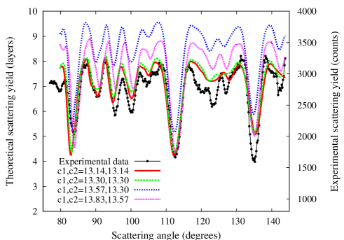
On first viewing the incorporation of strain appears to make the fit worse (compare with the fit for the 112 cell in Fig. 5). The region with a scattering angle in the approximate range 117∘-129∘ is especially bad. The scattering plane is shown schematically in Fig. 9. We can see from this that in the regions where the fit is bad it is the positions of the silicon atoms that are responsible for the poor fit of the blocking dips. Another minor silicon atom blocking dip at around 107∘ is also a poor fit. Given that the positions and the thermal vibrations of the silicon atoms have not been optimised it is no surprise that the fit is made worse by the introduction of strain.
However, the blocking dips produced by this structure are dominated by those caused by holmium atoms and close inspection of the major blocking dips at roughly 82∘, 113∘ and 135∘ supports the possibility of strain in these structures. The detail around these blocking dips is shown in Fig. 10. In the strained cells as the -axes are changed from the unrealistically low value obtained in the fit on an unstrained cell (13.14 Å) through the bulk silicide value (13.30 Å) and into the two cases where the -axis is expanded the blocking dip is shifted to become closer and closer to the experimentally measured dip. Indeed, at 84∘ and 113∘ the blocking dip for the strained cells is a better fit to experiment than that for the unstrained, fully optimised and multilayer averaged fit.
Thus far, the question of the surface termination has not been addressed. The unit cells involved in the simulations are holmium terminated which is not physically reasonable. Also, the LEED pattern shows a periodicity which is not accounted for in any of the simulated cells. We have attempted to investigate the surface termination but the simulated blocking curves show very little sensitivity to an extra layer of silicon atoms that form a surface termination. Other experiments that are more sensitive to the very top atomic layer may be better suited to resolving the issue of the surface termination (such as MEIS itself at normal incidence with 50 keV He+ ions).
V Lower Coverages
The work presented here suggests that at a coverage of 6 ML and under our preparation conditions strained tetragonal silicide islands are formed when holmium is grown on Si(100). At lower coverages (1 ML) nanowires form that are believed to be related to the hexagonal structure. The question naturally arises as to what structure forms in the intermediate coverage regime. Does the tetragonal structure grow atop the hexagonal phase? Or is there a phase change at a certain minimum coverage which results in tetragonal rather than hexagonal growth? To attempt to answer these question we have taken experimental data at a coverage of 3ML under the same growth conditions. Fig. 11 shows these data from the 3 ML sample compared with that from the sample grown using 6 ML of holmium.
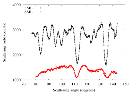
The principal blocking dips at 113∘ and 135∘ are present in both samples. In the 6 ML sample there are blocking dips at 90, 95 and 100 that are not produced from the 3 ML sample. If we refer to Fig. 9 we can see that these blocking dips are produced by holmium atoms in the upper region of the structure. We would not expect to see these features in a thinner silicide layer. In the hexagonal structure the dominant blocking dip is at a scattering angle of approximately 95∘ (see fig. 4). The simulations suggest that this feature should be present in hexagonal silicides that contain as few as 3 layers of holmium. We can see no evidence for any blocking dips in this region in the experiment with 3ML coverage and we must conclude that even at this coverage the structure is tetragonal.
VI Summary and Conclusion
Holmium silicide islands have been grown on the Si(100) surface and characterised using MEIS. Two structures have been fitted to the experimental data and this process clearly shows that under our growth conditions it is the tetragonal phase of the silicide that is formed and not the hexagonal phase and that these two structures do not coexist on the surface (the orthorhombic phase is too similar to the tetragonal phase for us to be able to determine if some of the orthorhombic nature of bulk HoSi is present in this surface tetragonal phase). A further experiment using a lower holmium coverage of 3 ML has also been shown to have the tetragonal structure which confirms that the hexagonal phase is not the phase adopted at low coverages in this system.
Other authors have reported growth of the hexagonal phase under similar growth conditions for some of the other RE silicides. It is interesting to speculate as to why similar experiments have reached different structural conclusions. It would appear that the structure that is formed is very sensitive to the growth conditions. Island morphology is very sensitively dependent upon the particular RE metal deposited and the annealing temperature used. In the paper by He et al. He et al. (2004) they report a deposition rate of 0.5 ML per minute during the formation of DySi2 whereas Ye et al. Ye et al. (2006a) report 0.3 ML per minute. It could be that the mobility of the RE metal and/or the lattice mismatch anisotropy of the particular silicide in question are important enough factors during the very early stages of silicide formation to dictate the final structure.
Using a simple 112 tetragonal unit cell the structure fitting suggests a -axis value that is too small to be physically reasonable when compared to the bulk structure. The blocking curves from a large 2500 atom 10102 nanoisland with lateral strain relaxation as a function of the distance from the interface have been simulated. The major blocking dips produced by this structure are a better fit to the experimental data than those produced by a non-strained periodic structure. The lesser blocking dips produced by silicon atoms in the simulations do not show good agreement with experiment. This is to be expected because the thermal vibrations and the positions of these atoms have not been optimised in the structure fit. The results of the comparison of MEIS data with simulations clearly show that a physically reasonable -axis value for the holmium silicide can only be obtained if the islands are strained to fit the Si(100) at the interface and the strain allowed to relax towards the top of the islands.
A full structural fit for this system would require an optimisation of the experiment-theory match with respect to all of the lateral and vertical spacings in the unit cell and their variation with distance from the interface, taking into account lateral strain relief, vertical relaxation and the particular vibrations of each individual atom. This task is not currently tractable in terms of computational resources and the available computer codes.
Acknowledgements.
The authors would like to acknowledge the Engineering and Physical Science Research Council for funding this research. Paul Quinn and the FOM Institute are thanked for supplying the XVegas and Vegas simulation codes. The assistance and technical support of Kevin Connell and Mark Pendleton are also much appreciated.References
- Preinesberger et al. (1998) C. Preinesberger, S. Vandré, T. Kalka, and M. Dähne-Prietsch, J. Phys. D: Appl. Phys. 31, L43 (1998).
- Kirakosian et al. (2002) A. Kirakosian, J. L. McChesney, R. Bennewitz, J. N. Crain, J.-L. Lin, and F. J. Himpsel, Surf. Sci. 498, L109 (2002).
- McChesney et al. (2002) J. L. McChesney, A. Kirakosian, R. Bennewitz, J. N. Crain, J. L. Lin, and F. J. Himpsel, Nanotechnology 13, 545 (2002).
- Chen et al. (2002a) Y. Chen, D. A. A. Ohlberg, and R. S. Williams, J. Appl. Phys. 91, 3213 (2002a).
- Lee and Kim (2003) D. Lee and S. Kim, Appl. Phys. Lett. 82, 2619 (2003).
- Liu and Nogami (2003a) B. Z. Liu and J. Nogami, Nanotechnology 14, 873 (2003a).
- Chen et al. (2003) Y. Chen, D. A. A. Ohlberg, G. Medeiros-Ribeiro, and R. S. Williams, J. Crystal Growth 251, 657 (2003).
- Nogami et al. (2001) J. Nogami, B. Z. Liu, M. V. Katkov, C. Ohbuchi, and N. O. Birge, Phys. Rev. B 63, 233305 (2001).
- Liu and Nogami (2001) B. Liu and J. Nogami, Surf. Sci. 488, 399 (2001).
- Liu and Nogami (2003b) B. Z. Liu and J. Nogami, J. Appl. Phys. 93, 593 (2003b).
- Chen et al. (2000) Y. Chen, D. A. A. Ohlberg, G. Medeiros-Ribeiro, Y. A. Chang, and R. S. Williams, Appl. Phys. Lett. 76, 4004 (2000).
- Chen et al. (2002b) G. Chen, J. Wan, J. Yang, X. Ding, L. Ye, and X. Wang, Surf. Sci 513, 203 (2002b).
- Cai and Zhou (2004) Q. Cai and W. Zhou, J. Phys.: Condens. Matter 16, 6835 (2004).
- Ohbuchi and Nogami (2002) C. Ohbuchi and J. Nogami, Phys. Rev. B 66, 165323 (2002).
- Katkov and Nogami (2002) M. Katkov and J. Nogami, Bull. Am. Phys. Soc. 47, 283 (2002).
- Frangis et al. (1996) N. Frangis, G. V. Tendeloo, J. V. Landuyt, G. Kaltsas, A. Travlos, and A. G. Nassiopoulos, Phys. Stat. Sol. (a) 158, 107 (1996).
- Frangis et al. (1997) N. Frangis, J. V. Landuyt, G. Kaltsas, A. Travlos, and A. G. Nassiopoulos, J. Crystal Growth 172, 175 (1997).
- Chen et al. (1998) J. C. Chen, G. H. Shen, and L. J. Chen, J. Appl. Phys. 84, 6083 (1998).
- Chen et al. (2002c) G. Chen, X. Ding, Z. Li, and X. Wang, J. Phys.: Condens. Matter 14, 10075 (2002c).
- Chi et al. (2003) K. S. Chi, W. C. Tsai, and L. J. Chen, J. Appl. Phys. 93, 153 (2003).
- Kuzmin et al. (2004) M. Kuzmin, P. Laukkanen, R. E. Perala, R. L. Vaara, and I. J. Varyrynen, Appl. Surf. Sci. 222, 394 (2004).
- He et al. (2004) Z. He, D. J. Smith, and P. A. Bennett, Phys. Rev. B 70, 241402(R) (2004).
- Harrison and Boland (2005) B. C. Harrison and J. J. Boland, Surf. Sci. 694, 93 (2005).
- Pető et al. (2005) G. Pető, G. Molnár, Z. E. Horváth, C. S. Daróczi, E. Zsoldos, and J. Gyulai, Surf. Sci. 578, 142 (2005).
- Tsai et al. (2005) W. C. Tsai, H. C. Hsu, H. F. Hsu, and L. J. Chen, Appl. Surf. Sci. 244, 115 (2005).
- Pasquali and Nannarone (2005) L. Pasquali and S. Nannarone, Nucl. Instrum. Methods Phys. Res. B 230, 340 (2005).
- Ye et al. (2006a) G. Ye, J. Nogami, and M. A. Crimp, Thin Solid Films 497, 48 (2006a).
- Ye et al. (2006b) G. Ye, M. A. Crimp, and J. Nogami, Mater. Res. Soc. Symp. Proc. 901, Ra13 (2006b).
- Maex and Rossum (1995) K. Maex and M. V. Rossum, eds., Properties of Metal Silicides (Institution of Engineering and Technology, 1995).
- Bonet et al. (2005) C. Bonet, I. M. Scott, D. J. Spence, T. J. Wood, T. C. Q. Noakes, P. Bailey, and S. P. Tear, Phys. Rev. B 72, 165407 (2005).
- Wood et al. (2006) T. J. Wood, C. Bonet, T. C. Q. Noakes, P. Bailey, and S. P. Tear, Phys. Rev. B 73, 235405. (2006).
- Spence et al. (2000a) D. J. Spence, S. P. Tear, T. C. Q. Noakes, and P. Bailey, Phys. Rev. B 61, 5707 (2000a).
- Spence et al. (2002) D. J. Spence, T. C. Q. Noakes, P. Bailey, and S. P. Tear, Surf. Sci. 512, 61 (2002).
- Spence et al. (2000b) D. J. Spence, T. C. Q. Noakes, P. Bailey, and S. P. Tear, Phys. Rev. B 62, 5016 (2000b).
- Wood et al. (2005) T. J. Wood, C. Bonet, T. C. Q. Noakes, P. Bailey, and S. P. Tear, Surf. Sci. 598, 120 (2005).
- Frenken et al. (1986) J. W. M. Frenken, J. F. van der Veen, and R. M. Tromp, Nucl. Instrum. Methods Phys. Res. B 17, 334 (1986).