Non-invasive detection of molecular bonds in quantum dots
Abstract
We performed charge detection on a lateral triple quantum dot with star-like geometry. The setup allows us to interpret the results in terms of two double dots with one common dot. One double dot features weak tunnel coupling and can be understood with atom-like electronic states, the other one is strongly coupled forming molecule-like states. In nonlinear measurements we identified patterns that can be analyzed in terms of the symmetry of tunneling rates. Those patterns strongly depend on the strength of interdot tunnel coupling and are completely different for atomic- or molecule-like coupled quantum dots allowing the non-invasive detection of molecular bonds.
pacs:
73.21.La, 73.23.Hk, 73.63.KvQuantum dots are often called artificial atoms Kouwenhoven et al. (1997) due to their discrete electronic level spectrum. When several quantum dots are connected, they start to interact van der Wiel et al. (2003). If the tunneling rate between the dots is small, the electronic wavefunctions are still constricted to the single quantum dots and the interaction is dominated by electrostatics with sequential interdot tunneling. In contrast, for large tunneling rates electronic states can be found extended over several dots. These extended states introduce covalent bonding as in real molecules Blick et al. (1996). Whether or not the interdot tunneling rates are sufficient to form coherent molecule-like states is a crucial information in order to properly describe a quantum dot system. Especially for quantum computing purposes Loss and DiVincenzo (1998) coherent states are necessary to form and couple qubits and to implement SWAP gates for qubit manipulation Petta et al. (2005); Hanson et al. (2007).
With dc-transport experiments there are only a few methods that can give hints for molecular bonds. The width of anticrossings visible in charging diagrams is a measure Golden and Halperin (1996), although anticrossings appear for capacitively coupled dots as well. In addition the curvature of the lines forming an anticrossing can be used Blick et al. (1998) and also the visibility of lines in non-parallel quantum dots Rogge et al. (2004). Another alternative is to study excited states. Strongly coupled quantum dots form bonding and antibonding states that are visible in nonlinear measurements Hüttel et al. (2005).
We have studied the impact of the coupling strength on the mean charge of multiple quantum dot systems coupled in series. Using a quantum point contact Field et al. (1993) we analyzed the mean charge in stability diagrams. We found that depending on the symmetry of tunneling rates and on the coupling strength characteristic patterns are formed in nonlinear measurements. This allows to non-invasively detect the symmetry of tunneling rates and the quality of the interdot coupling.
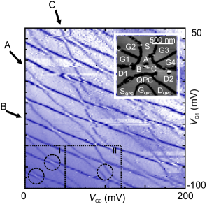
The measurements were performed on a device containing three quantum dots A, B and C (see inset of Fig. 1). The device was produced using local anodic oxidation on a GaAs/AlGaAs-heterostructure Ishii and Matsumoto (1995); Keyser et al. (2000). The three dots are positioned in a star-like geometry with one lead for each dot (Source S at A, Drain1 D1 at B and Drain2 D2 at C). The barriers and the potentials can be tuned with four sidegates G1 to G4. A quantum point contact (QPC) is placed next to the three dots for charge detection. The device is described in detail in Ref. Rogge et al. (2008).
Figure 1 shows a charging diagram of the triple dot device as a function of the voltages applied to gates G3 and G1. The derivative of the QPC-current with respect to is plotted. Dark lines correspond to an increase of charge detected by the QPC (e.g. charging a dot with an electron), bright features appear when the QPC detects a decrease of charge. Three sets of lines are visible that denote charging of the three dots. Lines with a shallow slope correspond to dot B, those with steap slopes appear due to charging of dot C. Intermediate slopes correspond to dot A. Whenever two lines from different sets intersect, an anticrossing appears due to finite coupling between the dots. At these anticrossings, two of the dots are in resonance and can thus be treated as double quantum dot. From transport measurement we know that the double dots A-B and A-C feature finite interdot tunnel coupling, while the double dot B-C is coupled capacitively only (see Ref. Rogge et al. (2008)). Therefore B-C is not interesting for the purpose of this paper. In the following we concentrate on the analysis of the two double dots A-B and A-C. This analysis is done in the two sections I and II with I showing anticrossings due to resonance of dots A and B, II showing an anticrossing due to resonance of dots A and C (circles).
Figure 2 shows three graphs measured in the region of section I. Charge detection is performed in the linear regime with (center image) and in the nonlinear regime with mV (left) and mV (right). While the center image shows the same pattern as observed in Fig. 1 with two sets of lines for dots A and B and two anticrossings, the situation changes in the nonlinear regime showing a more complex pattern with ground and excited states. The anticrossings appear shifted to the upper left for mV and to the lower right for mV. A triangular shaped pattern with additional lines is connected to the right ( mV) and to the left respectively ( mV). These triangles are familiar from nonlinear transport measurements in weakly coupled quantum dots Dixon et al. (1996); van der Wiel et al. (2003) and have recently been measured with charge detection as well Johnson et al. (2005). However, triangles with such patterns have not been reported so far. Dark and bright features alternate corresponding to alternating increase and decrease of mean charge measured with the QPC.
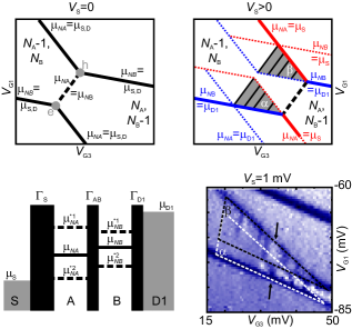
The origin of this pattern is explained with the schematics shown in Fig. 3. Assuming the total number of electrons to be or on dot A and or on dot B with ground state energies or and or , two transitions are possible:
If these chemical potentials equal those of the leads ( and ) lines are visible in the charging diagram. At (left schematic) and are degenerate. Therefore each chemical dot potential produces a single line forming the typical hexagonal cells with the so called triple points (marked with e and h) at the edges. At e transport through the serial double quantum dot can be described by sequential tunneling of one electron at a time through the otherwise empty dot states. At h transport occurs by sequential tunneling of one hole at a time through the otherwise filled dot states. In between the two triple points the chemical potentials of both dots are equal () and an electron can move from dot B to dot A with increasing . As dot A is further away from the QPC, the QPC detects a decrease of charge. Thus a white feature is visible at the anticrossings in the center image of Fig. 2.
The nonlinear regime is described with the schematic on the right (). The discussion for is analog. At the degeneracy of and is lifted, . Therefore there are two possible resonance conditions for each chemical dot potential. But as each dot does only couple to one lead, only one resonance condition per dot is relevant. Thus still only one line is visible per ground state transition (with and ). The other resonance conditions do not appear (dotted lines). However, as the two dots use different chemical lead potentials the anticrossings are shifted to the lower right as observed in the right image of Fig. 2. Therefore the exchange of an electron between the dots does not appear at , but at the dashed black line (right schematic). Left to this line there are two triangles (grey) where both chemical potentials, and , are between and and (Fig. 3, bottom left). These are the triangles described above. At the left border of these triangles the resonance condition is fulfilled opening a transport channel. Further transport channels within the triangles can appear due to excited atomic states.
As an example we take into account two excited states per dot with total energies and . Now two additional transitions are possible for each dot with new chemical potentials (Fig. 3, bottom left):
Additional transport channels form for , if the following resonance conditions are fulfilled (other channels are forbidden due to trapping):
Together with the resonance condition those are the four solid lines drawn in each grey triangle in the schematic. They can appear in conductance measurements with electron-like transport in triangle and hole-like transport in triangle .
With charge detection resonances are only visible, if they feature
a different mean charge than what is given in the grey regions.
Within the grey triangles at electrons can enter
dot B via Drain1, holes can enter dot A via Source (electrons can
leave A). Off resonance no transport between the dots is possible.
Therefore the mean charge in the grey regions, added to the charge
background of and electrons, is one
electron on dot B. On resonance, transport between the dots is
possible. Now the mean charge depends on the symmetry of the
tunneling rates between Source and dot A,
between Drain1 and dot B and the interdot
tunneling rate . Three different symmetries
are possible that define the mean charge on resonance within
triangles and
:
(i) , :
: one electron on B.
: one electron on B.
(ii) , :
: no electron on A and B.
: one electron equally occupying both dots.
(iii) , :
: one electron equally occupying both dots.
: one electron on both dots each.
In (i) no lines are visible with charge detection as the mean
charge on resonance is identical to the mean charge off resonance
in the grey regions. In (ii) and (iii) a resonance changes the
mean charge in both triangles and becomes visible. Thus it is much
more probable to observe excited states in weakly coupled double
dots than in single dots, where excited states can only appear
with symmetric tunneling rates Rogge et al. (2005).
Therefore (ii) or (iii) must be true for the measurements presented in Fig. 2. A more detailed analysis reveals the actual ratio of tunneling rates. The bottom of Figure 3 shows a section of the right image in Fig. 2 with the triangles and marked with white and black lines. As the difference between and is bigger than the splitting of the anticrossing, both triangles overlap. Within the triangles the additional lines are visible. Following the line marked with arrows from bottom to top, one first observes a dark feature in triangle and then a bright feature in triangle . Thus the effect on the mean charge must be vice versa in both triangles. This is only possible in (iii) with a decrease of mean charge in (iii) (as dot B is closer to the QPC than dot A) and an increase in (iii).
Within the overlapped region an electron can enter the possibly empty dots via Drain1, as the system is within triangle . This electron can now leave the dots again via Source, or another electron can enter via Drain1, as the system is in triangle as well. As , it is much more probable for a second electron to enter the system than for the first one to leave. Therefore the process related to triangle is favored.
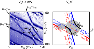
Triangular patterns are visible for A-B over a wide range of parameters. They finally fade out with increasing gate voltages as the tunneling rates are changed. In contrast no such patterns appear for A-C, although measured under the same conditions within the same device. Instead a different pattern is found. The left of Figure 4 shows a measurement at mV, taken within section II (as the lines of dot A appear steeper than those of B, but shallower than those of C, patterns of A-B at must be compared with patterns of A-C with ). The measurement shows an anticrossing (circle), that is almost not shifted compared to the one observed at (see Fig. 1). Another striking feature is the step that appears on the left of the anticrossing (ellipse). The left line of the anticrossing disappears and comes up again with a huge offset to the left. There are no triangular shaped patterns or lines for excited states.
The origin of this pattern is described using the schematic at the right of Fig. 4 assuming molecular bonds. With a relative width of anticrossings of (with 1 being the maximum Golden and Halperin (1996)) the double dot A-C is coupled stronger than A-B, which has a relative width of ca. 0.33. As for the schematics shown before for the resonances for ground state transitions split into two resonances as the chemical potentials in the leads differ. Here with resonances with appear shifted to the lower left compared to those with . Far off the anticrossing states of the two dots can be described as atomic with chemical potentials and . As dot A is coupled to Source and C to Drain2, the resonances and must appear (solid straight lines). Due to the strong coupling of A and C the pattern around the anticrossing cannot be described with atomic states any longer. Instead a common symmetric molecular state with energy evolves that is extended over the whole double dot. With the double dot energies for no added electrons and for two electrons added, two new transitions are possible:
These new chemical potentials can create two resonances each, one with , one with . Which of those involves a change of the mean charge depends on the tunneling rates again. If , charging appears at resonance with . If , charging appears at resonance with instead. The latter case results in the two curved solid lines in the schematic, that properly describes the experiment. In the area close to the anticrossing the double dot shows charging at resonance with as well as dot C far off the anticrossing. Dot A shows charging at resonance with instead. Therefore a jump must occur when the system changes from the molecular common state to the atomic state of dot A. Two of those jumps are shown in the schematic, but only one is visible in the measurement as the other one is disturbed by a line of dot B. However, the symmetry of tunneling rates is detected for double dot A-C as well.
Thus with charge measurements it is possible to detect the symmetry of tunneling rates for weakly and for strongly coupled double quantum dots. For the two double dots in this device the same symmetry was detected: , . However, depending on the strength of tunnel coupling two completely different patterns were found. Thus non-invasive charge measurement is capable of detecting molecular bonds in quantum dots.
For the heterostructure we thank M. Bichler, G. Abstreiter, and W. Wegscheider. This work has been supported by BMBF via nanoQUIT.
References
- Kouwenhoven et al. (1997) L. P. Kouwenhoven, C. M. Marcus, P. L. McEuen, S. Tarucha, R. M. Westervelt, and N. S. Wingreen, in Mesoscopic Electron Transport, edited by L. L. Sohn, L. P. Kouwenhoven, and G. Schön (Kluwer, Dordrecht, 1997), vol. 345 of Series E, pp. 105–214.
- van der Wiel et al. (2003) W. G. van der Wiel, S. D. Franceschi, J. M. Elzerman, T. Fujisawa, S. Tarucha, and L. P. Kouwenhoven, Rev. Mod. Phys. 75, 1 (2003).
- Blick et al. (1996) R. H. Blick, R. J. Haug, J. Weis, D. Pfannkuche, K. v. Klitzing, and K. Eberl, Phys. Rev. B 53, 7899 (1996).
- Loss and DiVincenzo (1998) D. Loss and D. P. DiVincenzo, Phys. Rev. A 57, 120 (1998).
- Petta et al. (2005) J. R. Petta, A. C. Johnson, J. M. Taylor, E. A. Laird, A. Yacoby, M. D. Lukin, C. M. Marcus, M. P. Hanson, and A. C. Gossard, Science 309, 2180 (2005).
- Hanson et al. (2007) R. Hanson, L. P. Kouwenhoven, J. R. Petta, S. Tarucha, and L. M. K. Vandersypen, Rev. Mod. Phys. 79, 1217 (2007).
- Golden and Halperin (1996) J. M. Golden and B. I. Halperin, Phys. Rev. B 54, 16757 (1996).
- Blick et al. (1998) R. H. Blick, D. Pfannkuche, R. J. Haug, K. v. Klitzing, and K. Eberl, Phys. Rev. Lett. 80, 4032 (1998).
- Rogge et al. (2004) M. C. Rogge, C. Fühner, U. F. Keyser, and R. J. Haug, Appl. Phys. Lett. 85, 606 (2004).
- Hüttel et al. (2005) A. K. Hüttel, S. Ludwig, H. Lorenz, K. Eberl, and J. P. Kotthaus, Phys. Rev. B 72, 081310(R) (2005).
- Field et al. (1993) M. Field, C. G. Smith, M. Pepper, D. A. Ritchie, J. E. F. Frost, G. A. C. Jones, and D. G. Hasko, Phys. Rev. Lett. 70, 1311 (1993).
- Ishii and Matsumoto (1995) M. Ishii and K. Matsumoto, Jpn. J. Appl. Phys. 34, 1329 (1995).
- Keyser et al. (2000) U. F. Keyser, H. W. Schumacher, U. Zeitler, R. J. Haug, and K. Eberl, Appl. Phys. Lett. 76, 457 (2000).
- Rogge et al. (2008) M. C. Rogge and R. J. Haug, Phys. Rev. B 77, 193306 (2008).
- Dixon et al. (1996) D. Dixon, L. P. Kouwenhoven, P. L. McEuen, Y. Nagamune, J. Motohisa, and H. Sakaki, Phys. Rev. B 53, 12625 (1996).
- Johnson et al. (2005) A. C. Johnson, J. R. Petta, C. M. Marcus, M. P. Hanson, and A. C. Gossard, Phys. Rev. B 72, 165308 (2005).
- Rogge et al. (2005) M. C. Rogge, B. Harke, C. Fricke, F. Hohls, M. Reinwald, W. Wegscheider, and R. J. Haug, Phys. Rev. B 72, 233402 (2005).