Highly-flexible wide angle of incidence terahertz metamaterial absorber
Abstract
We present the design, fabrication, and characterization of a metamaterial absorber which is resonant at terahertz frequencies. We experimentally demonstrate an absorptivity of 0.97 at 1.6 terahertz. Importantly, this free-standing absorber is only 16 microns thick resulting in a highly flexible material that, further, operates over a wide range of angles of incidence for both transverse electric and transverse magnetic radiation.
The initial impetus driving metamaterials research was the realization that a negative refractive index n = could be obtained by creating subwavelength composites where the effective permittivity and effective permeability are independently specified smith1 ; shelby ; veselago . Additionally, metamaterials allow for tailoring the impedance Z = in a manner not easily achieved with naturally occurring materials. This newfound approach to engineering n and Z offers unprecedented opportunities to realize novel electromagnetic responses from the microwave through the visible. This includes cloaks, concentrators, modulators, spoof plasmons, with many more examples certain to be discovered in the coming years schurig06a ; pendry06 ; rahm2008 ; padilla06 ; chen06 ; garcia-vidal05 .
Quite recently, there has been considerable interest in creating resonant metamaterial absorbers which, through judicious design of n and Z, offer the potential for near unity absorption landy07 ; tao08 ; landy2008 . The idea is to minimize the transmission and to simultaneously minimize, through impedance matching, the reflectivity. This has been experimentally demonstrated at microwave and terahertz frequencies landy07 ; tao08 ; landy2008 . Recently, other approaches have been theoretically put forward to extend these ideas to higher frequencies or to increase range of angles of incidence over which the absorptivity remains sufficiently large for applications diem2008 ; puscasu2008 ; avitzour2008 .
While the idea of designing a resonant absorber could be of potential use throughout the electromagnetic spectrum, this concept is expected to be especially fruitful at terahertz frequencies where it is difficult to find strong absorbers. Such absorbers would clearly be of use for thermal detectors or as a coating material to mitigate spurious reflections using continuous wave sources such as quantum cascade lasers landy07 ; tao08 ; williams06 ; tonouchi07 . Progress has been promising where the initial design yielded an absorptivity of 0.70 at 1.3 THz tao08 . This work has been extended to a polarization insensitive design with a demonstrated absorptivity of 0.65 at 1.15 THz landy2008 .
In this letter, we experimentally demonstrate a resonant metamaterial with an absorptivity of 0.97 at 1.6 THz. In comparison to previous designs tao08 ; landy2008 , the current design has several important advantages. Most importantly, the present design is on a freestanding highly-flexible polyimide substrate 8m thick which enables its use in nonplanar applications as it can easily be wrapped around objects as small a 6 mm in diameter. In addition, we demonstrate, through simulation and experiment, that this metamaterial absorber operates over a very wide range of angles of incidence for transverse electric (TE) and transverse magnetic (TM) configurations. Finally, the bottom layer of the absorber consists of a continuous metal film which simplifies the fabrication in that, for this two layer structure, precise alignment between the layers is not required. We also discuss the relative importance of losses in the metal and dielectric spacer layer.
Maximizing the absorption A is equivalent to minimizing both the transmission T and reflectivity R in that A 1 - T - R. As has been demonstrated landy2008 , in the limit that impedance matching to free space is achieved (i.e. Z = Zo resulting in R 0), the transmission reduces to T exp(-2n2dk)= exp(-d) where k is the free space wave vector, d is the sample thickness, n2 is the imaginary part of the refractive index, and is the absorption coefficient. Thus, impedance matching is a crucial step yielding a transmission that is determined solely by the losses in the slab of thickness d. In the case of a metamaterial absorber the effective n2 is determined by and . Thus, the design of a near-unity resonant metamaterial absorber, and must be optimized such that, at the desired center frequency, Z = Zo with n2 as large as possible.
A compact metamaterial absorber consists of two metallic layers separated by a dielectric spacer. The top layer consists of an array of split ring resonators which is primarily responsible for determining while the bottom metallic layer is designed such that the incident magnetic field drives a circulating currents between the two layers. However, given the strong coupling between the two layers, fine tuning of the geometry is required to obtain the conditions described in the previous paragraph. Fortunately, using full-wave electromagnetic simulation, rapid convergence to a near optimal design is readily achieved.
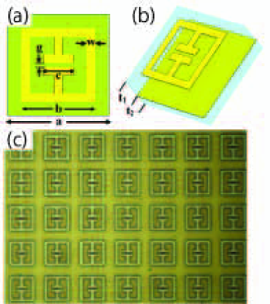
Figure 1 presents such an optimized design which we have subsequently fabricated and tested. The top layer (Fig. 1(a)) consists of an array of 200 nm thick Au electrically resonant split ring resonators schurigAPL ; padilla07 , with the dimensions as listed in the figure caption. In the absence of a second metallic layer, this structure yields a pure response, and can be thought of as an LC circuit as described elsewhere schurigAPL ; padilla07 . A dielectric spacer layer 8m thick separates the top and bottom metallic layers. The bottom metallic layer is a continuous 200 nm thick Au film. As Figure 1(b) shows, there is a second 8m thick dielectric layer which provides mechanical support but, being behind the continuous Au film, does not contribute to the electromagnetic response. Figure 1(c) shows a photograph of a portion of the structure we have fabricated and tested as detailed below.
The optimized structure presented in Figure 1 was obtained through computer simulations using the commercial program CST Microwave StudioTM 2006B.04. The frequency domain solver was utilized where the Au portions of the metamaterial absorber was modeled as lossy gold with a frequency independent conductivity = 4.09107 S/cm. The 8m thick dielectric layer was modeled using the experimentally measured value of polyimide as this is what is used in the subsequent fabrication. Specifically, a frequency independent + i 2.88 +i0.09 was used which corresponds to a loss tangent tan() / 0.0313 tao08b . The amplitude of the transmission S21 and reflection S11 were obtained and the absorption was calculated using A = 1-R-T = 1-S-S where, as expected for the present design, S21 is zero across the entire frequency range due to the ground plane. The optimized structure presented in Fig. 1 was obtained (simulating radiation at normal incidence) through parameter sweeps of the dimensions of the SRR and the dielectric spacer thickness. The optimized parameters are those which yielded the lowest reflectivity at the design frequency of 1.6 THz.
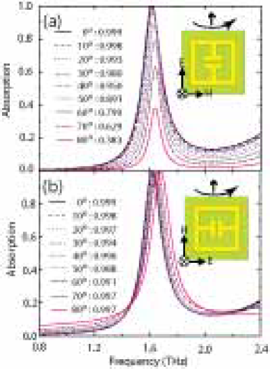
The simulated absorption as a function of frequency for the optimized structure (Fig. 1) is presented in Figure 2 for TE (Fig. 2(a)) and TM (Fig. 2(b)) radiation at various angles of incidence. For the TE case, at normal incidence a peak absorption of 0.999 is obtained. With increasing angle of incidence, the absorption remains quite large and is at 0.89 at 50o. Beyond this there is a monotonic decrease in the absorption as the incident magnetic field can no longer efficiently drive circulating currents between the two metallic layers. There is also a slight frequency shift of 30 GHz from 0o to 80o. For the case of TM radiation shown in Fig. 2(b), the absorption at normal incidence is 0.999 at normal incidence and remains greater than 0.99 for all angles of incidence. In this case, the magnetic field can efficiently drive the circulating currents at all angles of incidence which is important to maintain impedance matching. The frequency shift for TM radiation is 80 GHz from 0o to 80o. As these simulations reveal, this MM absorber operates quite well for both TE and TM radiation over a large range of angles of incidence.
An additional aspect to consider in the design of metamaterial absorbers are losses in the constituent materials comprising the structure. As discussed in the introduction, one of the design criteria is to obtain a large value of the imaginary part of the effective refractive index. This necessitates having some losses in the metal. Losses in the dielectric spacer are expected to contribute as well. For example, in the limit of a perfect electric conductor and a lossless dielectric, the absorption in the composite in Fig. 1 is zero. However, losses in gold are sufficient to yield a strong narrow band resonance as shown in Figure 2.
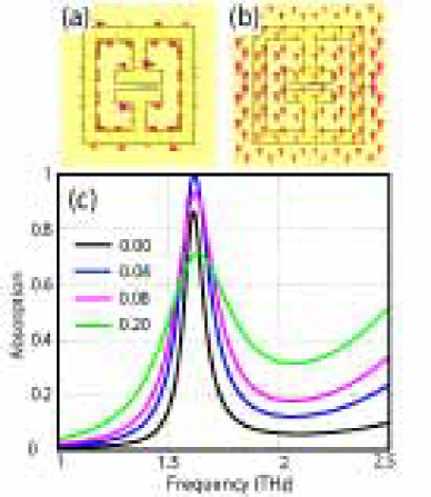
Fig. 3(a) and (b) show the calculated surface current density for a TE wave at resonance. The currents are in opposite directions on SRR and the ground plane as expected for a magnetic resonance. Figure 3(c) shows the absorption as a function of frequency for the design in Fig. 1. The black curve assumes a lossless dielectric - i.e. tan() = 0. In this case, the peak absorption is 0.88 which is smaller than the calculations in Figure 2. This suggests losses in the dielectric contribute to increasing the absorption. For example, increasing tan() to 0.04 (blue curve, Fig. 3(c)) increases the absorption to 0.99 which is an increase of 0.11 in comparison to a lossless dielectric. However, a point of diminishing return is reached for larger values of tan() (see Fig. 3(c)) in that the absorption decreases and the resonance broadens. These results suggest that optimization of tan() of the dielectric spacer can maximize the metamaterial absorption. Further, it appears the losses in polyimide (tan() 0.0313) should contribute 0.1 to the absorption of our metamaterial absorber as is evident by comparing the black curves in Fig. 2(a) and 3(c).
The free standing absorber structures were fabricated with a surface micromachining process on flexible polyimide substrate using a silicon wafer as the supporting substrate during the fabrication process. Liquid polyimide (PI-5878G, HD MicroSystemsTM) was spin-coated on a 2 inch silicon wafer to form the free standing substrate. In this work, the polyimide was spin-coated at 1,700 rpm and cured for five hours in an oven at 350 C in a nitrogen environment yielding an 8m thick polyimide layer. A 200 nm thick Au/Ti film was e-beam evaporated on the polyimide substrate to form the ground plane. Another 8m thick polyimide layer was spin coated on the top of the ground plane to form the polyimide spacer and processed according to the procedure mentioned above. For the SRR array, direct laser writing technology was chosen over traditional mask contact lithography technology to improve the patterning quality on the polyimide substrates. ShipleyTM S1813 positive photoresist was first calibrated and then exposed with a HeidelbergTM DWL 66 laser writer to pattern the top layer of electric ring resonators. Another 200 nm thick Au/Ti film was e-beam evaporated followed by rinsing in acetone for several minutes. The metamaterial absorber fabricated on the polyimide substrate was carefully peeled off of the silicon substrate at the end of fabrication. Our samples show great mechanical flexibility and can be easily wrapped around a cylinder with a radius of a few millimeters.
A Fourier transform infrared (FTIR) spectrometer was used to experimentally verify the behavior of the absorber by measuring the transmission and reflection over the frequency range of 0.6 THz to 3 THz with a resolution of 15 GHz. A liquid helium cooled bolometer detector and 6 m mylar beam splitter were used to optimize the FTIR performance over the frequencies measured. Prior to measurement, the free standing absorber samples were diced into 1 cm 1 cm squares. The aperture of the incident beam was 5 mm, which is considerably smaller than the sample dimension. The sample was mounted at normal incidence for the transmission measurement. As expected, the transmitted intensity was essentially zero due to the gold ground plane which blocks all radiation through the absorber. The achievable incident angle for reflection measurements is constrained within the range from 30 to 60 off-normal due to the experimental limitations. The measurements were performed with electric field perpendicular to the SRR gap to excite the electric resonance. The absorption spectrum was easily obtained from the reflection results (i.e. A 1-R).
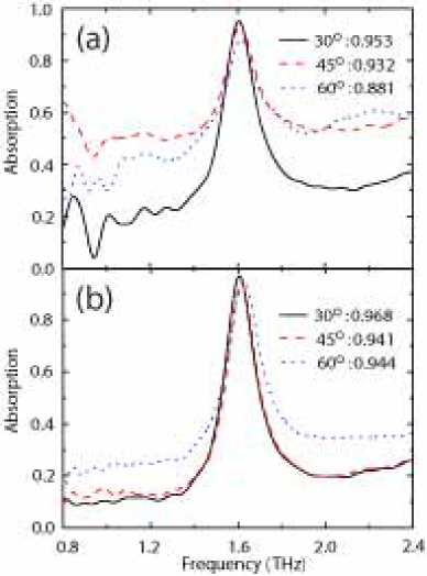
The experimental results are displayed in Figure 4(a) and (b) for TE and TM incident radiation, respectively. For the TE radiation, the absorption peaks at 0.95 for an angle of incidence of 30o decreasing slightly to 0.88 at 60o. This is in reasonable agreement with the simulations though the experimental absorptivity at 60o is 0.09 higher than for simulation. However, the off-resonance absorptivity is quite large in disagreement with the simulations. This may arise, in part, from scattering of radiation from imperfections arising from the fabrication. For the TM measurements the peak absorptivity is 0.968 at 30o angle of incidence and only drops by 0.024 upon increasing to 60o. Further, the increase in the baseline absorption is much smaller in comparison to the TE measurements and is in better agreement with simulations. A closer inspection of Fig. 4(b) also reveals a slight increase in the resonance frequency with increasing angle of incidence in agreement with simulation. Overall, these results substantially confirm the simulation results demonstrating that our MM absorber yields a large absorptivity over a broad range of angles of incidence for both TE and TM radiation.
In summary, we have presented the design, fabrication, and characterization of a highly flexible metamaterial absorber that, experimentally, obtains an absorptivity of 0.96 at 1.6 THz, and further, operates over wide angular range for TE and TM radiation. Such a composite THz metamaterial may find numerous applications ranging from the active element in a thermal detector to THz stealth technology.
We acknowledge partial support from the Los Alamos National Laboratory LDRD program, DOD/Army Research Laboratory W911NF-06-2-0040, NSF EECS 0802036, and DARPA HR0011-08-1-0044. The authors would also like to thank the Photonics Center at Boston University for all of the technical support throughout the course of this research.
References
- (1) D. R. Smith, W. J. Padilla, D. C. Vier, S. C. Nemat-Nasser, S. Schultz, Phys. Rev. Lett. 84, 4184 (2000).
- (2) V. G. Veselago, Soviet Physics USPEKI 10, 509 (1968).
- (3) R.A. Shelby, D.R. Smith, S. Schultz, Science 292, 77 (2001).
- (4) D. Schurig and J. J. Mock and B. J. Justice and S. A. Cummer and J. B. Pendry and A. F. Starr and D. R. Smith, Science 314, 977 (2006).
- (5) J. B. Pendry and D. Schurig and D. R. Smith, Science 312, 1780 (2006).
- (6) M. Rahm, S. A. Cummer, D. Schurig, J. B. Pendry, D. R. Smith, Phys. Rev. Lett. 100, 063903 (2008).
- (7) W. J. Padilla and A. J. Taylor and C. Highstrete and Mark Lee and R. D. Averitt, Phys. Rev. Lett. 96, 107401 (2006).
- (8) H-T Chen, W. J. Padilla, J. M. O. Zide, A. C. Gossard, A. J. Taylor, R. D. Averitt, Nature 444, 597 (2006).
- (9) F. J. Garcia-Vidal, L. Martin-Moreno, J. B. Pendry, J. Opt. A: Pure Appl. Opt. 7,, S97 (2005).
- (10) N. I. Landy and S. Sajuyigbe and J. J. Mock and D. R. Smith and W. J. Padilla, Phys. Rev. Lett. 100, 207402 (2008).
- (11) H. Tao, N. I. Landy, C. M. Bingham, X. Zhang, R. D. Averitt, W. J. Padilla, Opt. Express 75, 7181 (2008).
- (12) N. I. Landy, C. M. Bingham, T. Tyler, N. Jokerst, D. R. Smith, W. J. Padilla, http://arxiv.org/abs/0807.3390
- (13) M. Diem, T. Koschny, C. M. Soukoulis, http://arxiv.org/abs/0807.2479
- (14) I. Puscasu, W. L. Schaich, Appl. Phys. Lett. 92, 233102 (2008).
- (15) Y. Avitzour, Y. A. Urzhumov, G. Shvets, http://arxiv.org/abs/0807.1312
- (16) G. P. Williams, Rep. Prog. Phys. 69, 301 (2006).
- (17) M. Tonouchi, Nature Photonics 1, 97 (2007).
- (18) D. Schurig, J.J. Mock, and D.R. Smith, Appl. Phys. Lett. 88, 041109 (2005).
- (19) W. J. Padilla and M. T. Aronsson and C. Highstrete and M. Lee and A. J. Taylor and R. D. Averitt, Phys. Rev. B 75, 041102(R) (2007).
- (20) H. Tao, A. C. Strikwerda, K. Fan, C.M. Bingham, W. J. Padilla, X. Zhang, R. D. Averitt, http://arxiv.org/abs/0808.0454