Impact of the Meissner effect on magnetic micro traps for neutral atoms near superconducting thin films
Abstract
We theoretically evaluate changes in the magnetic potential arising from the magnetic field near superconducting thin films. An example of an atom chip based on a three-wire configuration has been simulated in the superconducting and the normal conducting state. Inhomogeneous current densities within the superconducting wires were calculated using an energy-minimization routine based on the London theory. The Meissner effect causes changes to both trap position and oscillation frequencies at short distances from the superconducting surface. Superconducting wires produce much shallower micro traps than normal conducting wires. The results presented in this paper demonstrate the importance of taking the Meissner effect into account when designing and carrying out experiments on magnetically trapped neutral atoms near superconducting surfaces.
I Introduction
Atom chips with microfabricated and nanofabricated field-generating elements are useful devices for the coherent manipulation of ultracold atoms Fortagh:07 . A diversity of potentials with high spatial resolution can be generated near the chip surface using state-of-the-art fabrication technology of metals, semiconductors, superconductors and optical waveguides. By means of these potentials Bose-Einstein condensates and degenerate Fermi gases are routinely prepared. Significant progress in coherent manipulation and state-sensitive detection of single atoms has been achieved in recent years Teper:06 ; Colombe:06 . Applications of atom chips include atom interferometers Wang:05 ; Schumm:05 ; Jo:07 ; G nther:07 , ultra sensitive magnetic field sensors Fortagh:02 ; Wildermuth:05 and portable experimental systems for quantum gases Du:04 .
A key role on atom chips is played by the atom-surface interactions, such as undesirable spin-decoherence mechanisms Henkel:99 and attractive Casimir-Polder forces Lin:04 ; Harber:05 . The lifetime of magnetic traps near the chip surface is limited by decoherence mechanisms produced by the near-field noise radiation from thermally induced currents in conductive surfaces Lin:04 ; Henkel:99 ; Jones:03 ; Rekdal:04 . Cooling the chip can reduce those thermal currents and thus increase the lifetime of the magnetic traps. An important increase in the lifetime of several orders of magnitude is expected when the surface layer crosses the transition from the normal to the superconducting state Hohenester:07 . The achievement of such conditions promises a new class of experiments with cold atoms integrated with nanostructured surfaces that will allow coherent control over the atoms into the submicron range. Exciting proposals for coupling atoms to nanodevices such as mechanical oscillators Treutlein:07 or superconducting circuits Singh:07 outline new perspectives on experimental research at the interface between atomic and solid-state physics.
Although the usage of superconducting microstructures on atoms chips was already proposed in 1995 by Weinstein and Libbrecht Weinstein:95 , and later on in several theoretical studies Scheel:05 ; Skagerstam:06 ; Hohenester:07 , the impact of the Meissner effect London:50 ; Ketterson:99 on the magnetic trapping potential has not been considered as yet. In this paper, we show that the magnetic-field expulsion from the superconductor has an important effect on the magnetic trap. Our theoretical results will be essential for the proper design of superconducting atom chips, a subject on which the first experimental results have recently been reported Roux:08 ; Mukai:07 .
Accurate methods to calculate the potential landscape near the chip surface is a prerequisite for cold-atom experiments on atom chips. In the case of using superconducting wires, these calculations must take into account the Meissner effect, which implies that the intensity of induced or applied currents decays exponentially into the interior of the superconductor with a penetration depth , which is also the depth to which the magnetic field penetrates the superconductor. Magnetic-field calculations are especially important at short distances from the chip surface, where atoms are not easily accessible by imaging methods and where the Meissner effect can have an important impact on the trap parameters.
The main goal of this paper is to investigate how the Meissner effect modifies magnetic traps near superconducting thin films. To accomplish this task, magnetic fields and trap parameters such as position, oscillation frequencies and trap depth were calculated in simulated chips containing thin-film wires. Simulations were carried out for the vortex-free superconducting state and for the normal conducting state, and the differences between the two cases are analyzed.
Current distributions in superconducting thin films were calculated in the frame of the London theory London:50 . Despite its fundamental nature, exact solutions of the London theory exist only for trivial cases such as a single sphere or a single cylinder in a homogeneous magnetic field London:50 . Numerical methods are therefore necessary to calculate current density distributions in thin-film microstructures. Brandt and Mikitik Brandt:00 reported on how to obtain numerical solutions of the London theory for strips with rectangular cross section in a perpendicular homogeneous magnetic field and/or with applied electric current. More general geometries can be solved using commercial programs which, however, have severe limitations. For example, most of them provide accurate solutions only if the thickness of the thin film is similar to the penetration depth Kapaev:96 . In the present paper we overcome this limitation and provide an algorithm that provides accurate solutions of the London theory by finding the current distribution that minimizes the free energy. A similar minimization method Pardo:03 has been used to obtain the magnetization curves of arrays of superconducting strips in homogeneous magnetic fields. The numerical method presented in this paper can solve more general geometries in arbitrary inhomogeneous magnetic fields, including most of the geometries that are typically present in atom chips.
II Magnetic confinement on an atom chip
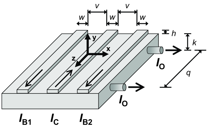
A magnetic micro trap can be realized with the atom-chip geometry represented in Fig. 1. Three parallel thin-film wires on the chip surface generate a two-dimensional confining field (magnetic guide). The current in the central wire is opposite in direction to the currents and in the two outer wires. The magnetic guide forms at the position , where the magnetic field of the central current is canceled by the bias field generated by and . The field forms a two-dimensional quadrupole field around . Its modulus increases linearly in the radial directions:
| (1) |
Here, is the gradient of the magnetic guide in the radial directions. For simplicity, these three parallel wires, which we will refer to as quadrupole wires, are assumed to be identical in size. The width and the thickness of each quadrupole wire are denoted by and , respectively. The outer wires are separated from the central wire by .
Longitudinal confinement is achieved by means of the inhomogeneous offset field generated by two offset wires perpendicular to the quadrupole wires. The two offset wires are located below the chip surface, and separated from the quadrupole wires by . They are driven with identical currents .
The offset field is superimposed onto the two-dimensional confining field , in such a way that a magnetic trap forms between the two offset wires around the point . Near the centre of the trap,
| (2) |
where and are the fist- and second-partial derivatives of with respect to the corresponding directions, evaluated at . The trap forms only if ; thus for distances smaller than about 0.6 . The offset field at the trap center normally suffices to prevent Majorana spin-flip transitions Sukumar:97 and the consequent loss of atoms in Bose-Einstein condensates. However, in experiments with thermal clouds at temperatures of several micro K, it might be necessary to externally apply an additional homogeneous offset field .
The centre of the trap
| (3) |
is slightly displaced from the position of the magnetic guide.
The offset field changes the radial potential from linear to parabolic, with a harmonic oscillation parameter . The magnetic trap is then characterized by the radial and longitudinal oscillation frequencies
| (4) |
Here, is the Landé factor, is the Bohr magneton, is the magnetic quantum number, and is the atom mass.
The component of causes a small rotation of the longitudinal axis of the magnetic trap. In the particular case that the magnetic trap is in the plane = 0, and thus , the quadrupole field can be expressed as
| (5) |
and the rotation occurs about the y axis Gunther:05 , with angle .
III Calculation of inhomogeneous current densities in superconducting thin films
Current densities are homogeneous in normally conducting wires. Inhomogeneous current densities in the superconducting wires were calculated numerically using the London theory. General solutions of the London theory for the microstructure shown in Fig. 1 can be obtained by linear superposition of two separate cases. The first of these describes the behavior of the microstructure when the three quadrupole wires carry the respective currents , and . The second case describes the behavior of the microstructure when each offset wire is driven with a current and no current is applied to the quadrupole wires. In the second case, induced screening currents in the quadrupole wires can modify the parameters of a magnetic trap formed near the chip surface.
For simplicity, the offset wires are assumed to be infinitely thin. This approximation is valid if the width of the offset wires is much smaller than , in which case neither the screening currents in the quadrupole wires nor the magnetic fields near the chip surface depends on the current distribution in the offset wires. The homogeneous offset field is not distorted by the Meissner effect because the longitudinal demagnetizing factor of a strip quickly tends to zero as the strip length increases to infinity Joseph:65 .
III.1 Applied currents in the quadrupole wires
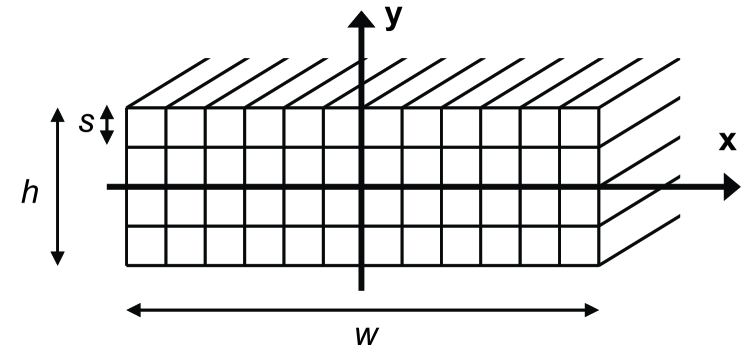
Current density distributions in the superconducting quadrupole wires are calculated with an energy-minimization numerical procedure. Every quadrupole wire is divided up into a large number of thin longitudinal strips with squared cross section of side (see Fig. 2). The current density is assumed homogeneous within each thin strip, although it may vary from strip to strip. The free energy of this system is the sum of the magnetostatic energy of the currents and the kinetic energy of the electrons Ketterson:99 , and can be written in the form
| (6) |
where is the electric current along the strip and is the mutual inductance between the strips and . The general expression for is Grover:46 ; Meservey:69
| (7) | |||||
where is the Kronecker delta, is the current density, and denotes the position of point within the strip . The first and second terms represent the magnetic and the kinetic inductances, respectively. The integrals are carried out over the volumes of the corresponding strips. Since the current density is homogeneous within each strip, the magnetic term can be approximated by classical formulas tabulated in Ref. Grover:46 . The integral of the kinetic term has a trivial solution. The matrix elements then become
| (8) |
where is the length of the wires and is the distance between the centers of the considered strips.
The superconducting current density is obtained by finding the set of values that minimize the function . This is accomplished with the method of the Lagrange multipliers, and imposing that the total current flowing in each wire is fixed. The constraints are
| (9) |
The equations to find the superconducting currents are
| (10) | |||||
where , and are the Lagrange multipliers. The solution of this system of linear equations is a set of values that represent the current distribution in the superconducting wires.
For long wires () the calculated current distribution does not depend on . This limit is valid in all the examples shown in this paper, where all wires are assumed infinitely long.
Low values of improve the accuracy of the solution at the expense of long computation time. We have found that all values lower than produce practically the same numerical results, and therefore, is in general a good choice for calculations.
Calculating the mutual inductance between two strips is not incompatible with the general definition of mutual inductance for two closed circuits. One can imagine that every quadrupole wire is part of a closed circuit that includes the current drivers and the wires between the chip and the drivers. The mutual inductance between two strips can be defined as the contribution of the two strips to the total mutual inductance between the closed circuits of which they form part.
III.2 Screening currents in the quadrupole wires
Screening currents arise in superconductors in the presence of external magnetic fields as a consequence of the Meissner effect. Screening currents can be calculated using the energy-minimization method described in this section. This numerical method requires to decompose the screening currents in small current elements . In a magnetostatic situation, the screening currents are closed, and therefore, a decomposition based on small magnetic dipoles or small closed current elements is the most appropriate.
The geometry of the closed current elements described in this paragraph is suitable to evaluate the energy and the flux including the kinetic term geometry . The superconducting body is divided up into small cubes of side . The current is assumed to be homogeneous within every small cube, although both the intensity and the direction of the current might vary from cube to cube. Closed current elements similar to magnetic dipoles are built by grouping the cubes in sets of four, in the way illustrated in Fig. 3. The centers of the four cubes lie in the same plane. Sets of four cubes can be built in planes parallel to the axis ( sets), to the axis ( sets) or to the axis ( sets). In this manner, any cube that is not on the wire surface belongs to twelve different sets: four sets, four sets and four sets. Sets are sorted with numbers. Every set has associated a current , being the number of the set. The current element is distributed within the set in a way that is similar to a magnetic dipole, as shown in Fig. 3. The current changes its direction by 90 degrees as it passes from a cube to the next cube of the set. The direction of in each cube is described by the unit vectors , , and .
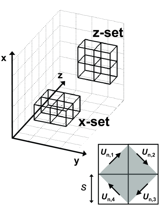
The mutual inductance between two sets and is obtained by summing the contributions of the mutual inductances between the separate cubes of both sets. Assuming one set made up of the cubes , , and and another set made up of the cubes , , and , the total mutual inductance between the two sets is
| (11) |
where
| (12) | |||||
is the contribution of the cubes and to . The scalar product accounts for the fact that this contribution depends on the angle between the current directions. Here, denotes the position of point within the cube , and is the current density in the set . The integrals are carried out over the volume of the corresponding cubes. The double integral of the magnetic term was calculated numerically Mathematica , and the integral of the kinetic term has a trivial solution. The matrix elements are then approximated by
| (13) |
where is the distance between cube centers.
For the reasons mentioned above, the mutual inductance between two cubes is a senseless physical idea unless each cube is regarded as part of a close circuit. To understand the meaning of , the screening current tubes can be regarded as a collection of closed circuits with a certain inductance matrix. In this way the mutual inductance between two cubes can be understood as the contribution made by the cubes to the total mutual inductance between the two current tubes in which the cubes are included. This idea also applies to the self-inductance.
Every set of cubes is also characterized by the effective surface , which is represented in Fig. 3 by the gray area. The effective surface is defined so that the product is the flux produced by through . The modulus of is 2, and its direction is determined by the right-hand rule from the direction of the current . Following the notation of Fig. 3, the effective surface can be expressed by .
The solution of the London theory for this system is the current distribution that cancels the flux -including both the magnetic and the kinetic terms- in the interior of the superconducting wires. It is possible to demonstrate London:50 that this condition is equivalent to the free-energy minimization performed in the previous section. The equations to be solved are formulated so that the flux through every set of cubes is null:
| (14) |
Here, is the total number of sets, symbolizes the elements of the inductance matrix, is the external magnetic field at the position of the set , and is the effective surface of the set . The first term in this equation represents the total flux induced by the screening currents onto the set . The second term is the magnetic flux of the external field onto the set .
Due to its large size, the matrix cannot be inverted using any of the mathematic programmes that are generally available. As an alternative, an iterative method has been used to solve Eq. (14). In the fist step, a homogeneous screening current distribution is assumed: ; . This distribution will not satisfy Eq. (14), and the flux created by the assumed screening currents onto each set will not cancel the flux created by the offset wires . In the second step, the current distribution is calculated by , which will generate a flux that will be more similar to the desired solution. The process continues until the convergence condition is satisfied: , after iterations. The number is a convergence factor that has no physical meaning. This value is chosen by trial and error. The best choice depends on the geometry of the superconducting body. If is too high, the method is not convergent; but if is too low, the convergence is very slow. can vary from set to set and also from step to step. The particular values of used for our calculations will not be shown here since the results do not depend on them and since there are many other possibilities.
Once the closed current elements have been obtained, the total current in every single cube is calculated by summing the contributions of the sets of which the cube forms part. From the total currents in the single cubes, the magnetic field outside the superconducting body can be calculated.
The method presented in this section can be used to calculate screening currents in superconducting thin-films induced by arbitrary inhomogeneous magnetic fields. In the example shown in Fig. 1, the magnetic field generated by the offset wires has no component along the direction. For that reason, only sets and sets are used.
IV Numerical results
In this section we assess how the Meissner effect alters the magnetic-trap parameters in the superconducting microstructure depicted in Fig. 1. In all the examples shown in this paper, the width of the quadrupole wires and the separation between them are m and m, respectively. The penetration depth in the superconducting wires is 100 nm, which is a typical value for metallic superconductors. The offset wires are at a distance of m underneath the quadrupole wires. The thickness of the quadrupole wires as well as the separation between the two offset wires will be varied in the examples in order to demonstrate their effect on the magnetic-trap parameters.
IV.1 Quadrupole magnetic guide generated by the superconducting chip
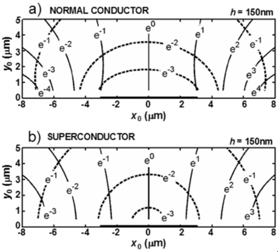
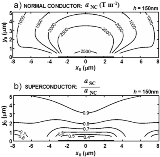
First we analyze the position of the magnetic guide in the plane. The magnetic guide can be positioned within a large area above the chip surface by changing the ratios
| (15) |
Figure 4 illustrates the trajectories corresponding to constant (dashed lines) and to constant (solid lines) for the superconducting and the normal conducting chip. Differences between the two cases are noticeable when the distance between the magnetic trap and the chip surface is smaller than the width of the wires.
In principle, both the position in the plane and the radial gradient of the quadrupole field depend on the applied currents , and . Once the ratios and have been chosen to position the magnetic guide, the radial gradient can be varied by changing the value of . Fig. 5(a) shows for constant 1 A the radial gradient in the normal conducting chip as a function of the position of the magnetic guide. The radial gradient for other values of can be obtained by linear scaling. For the superconducting case, the gradient was calculated in the same way, keeping at a constant value of 1 A. Figure 5(b) shows the ratio . Superconducting wires produce considerably lower radial gradients than normal conducting wires. The radial gradient of is related with the radial oscillation frequency of the micro trap by Eq. (4).
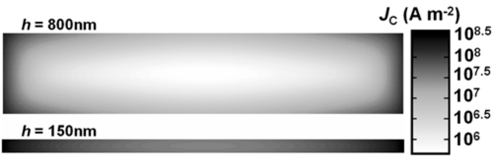
Changes in the trapping field caused by the Meissner effect become more pronounced when the superconducting wires are thicker or when the penetration depth is smaller. Either thinner wires or longer penetration depths imply more homogeneity in the superconducting current densities, which results in magnetic fields which are more similar to those produced by normal conductors. Figure 6 shows the current-density distribution along the central wire for two different thicknesses. Three regimes can be distinguished. If , the current density decays exponentially from the surface and shows a sharp peak in each corner. If , the current density becomes homogeneous along the axis, having two maxima at and . For extremely thin wires, the kinetic energy gets so high that the current density becomes almost homogeneous, allowing the magnetic flux to penetrate the film.
In the case of normal conducting wires, the magnetic-trap parameters were independent of the thickness . This is illustrated by comparing the numerical results obtained for different values of . The variations in the position and in the radial gradient produced by varying between 50m and 800m were, respectively, less than 0.01m and less than 0.1 at any position within the area represented in Figs. 4 and 5. On the contrary, our numerical calculations demonstrate that the magnetic-trap parameters depend considerably upon the value of the thickness when the chip is superconducting. For example, while for =150 nm the radial gradient in the superconducting chip is 0.4 times the radial gradient in the normal conducting chip at 0.5 m from the chip surface above the central wire (see Fig. 5), this reduction factor is 0.6 for =50 nm and 0.3 for =500nm at the same position. Therefore, the thickness of the thin-film wires becomes relevant in the superconducting state.
IV.2 Longitudinal confinement in the superconducting state
The analysis presented in this section is restricted to magnetic traps located in the plane = 0. Different distances from the chip surface will be considered.
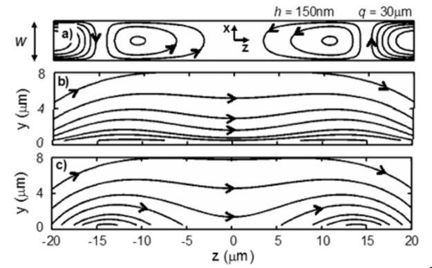
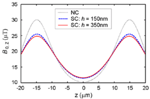
Figure 7 shows the screening currents in the central quadrupole wire as well as the magnetic field lines of the offset field for the superconducting and the normal conducting chip. Figure 8 represents the longitudinal component of the magnetic field calculated along the direction at m) for three different cases: normal conductor, superconductor with = 150 nm, and superconductor with = 350 nm. As with the results obtained for , differences between the superconducting and the normal conducting states become larger with increasing . The screening currents in the superconducting quadrupole wires reduce the z component of the magnetic field at the positions and . This effect entails a decrease of the trap depth along the longitudinal direction. This reduction is of about 15% at 2 from the surface, and becomes higher than 25% at distances of 1 or shorter. For above than 10 , the reduction is lower than 5%.
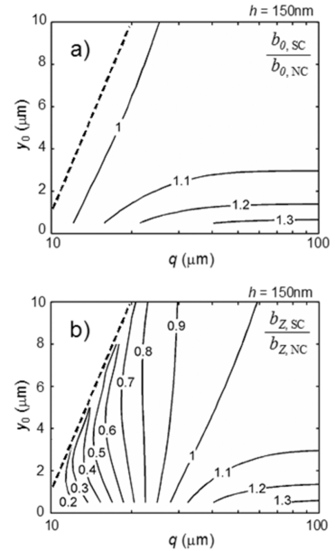
The parameters , and that describe the inhomogeneous offset field were numerically calculated for the superconducting chip (SC) and the normal conducting chip (NC) as a function of and . Figure 9(a) shows the ratio . The horizontal axis represents the distance between the two offset wires, and the vertical axis represents the position of the magnetic trap . As observed in this figure, the Meissner effect in the superconducting wires slightly increases the value of . This increase becomes more significant as the distance between the two offset wires gets longer, and the magnetic trap gets closer to the surface. Figure 9(b) shows the ratio . The longitudinal oscillation frequency of the microtrap is related to by means of Eq. (4). As seen in Fig. 9 the longitudinal frequency is dramatically reduced by the Meissner effect when the offset wires are close to each other. For high values of the effect is the opposite, and the longitudinal frequencies are slightly higher in the superconducting chip.
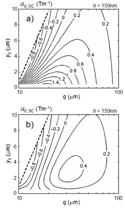
Figure 10 compares the value of between the superconducting and the normal conducting chips. The parameter is related with the angle of rotation of the trap as explained in Sec. II. The calculated values of were significantly lower in the superconducting microstructure than in the normal conducting microstructure.
V Simulation of a magnetic micro trap
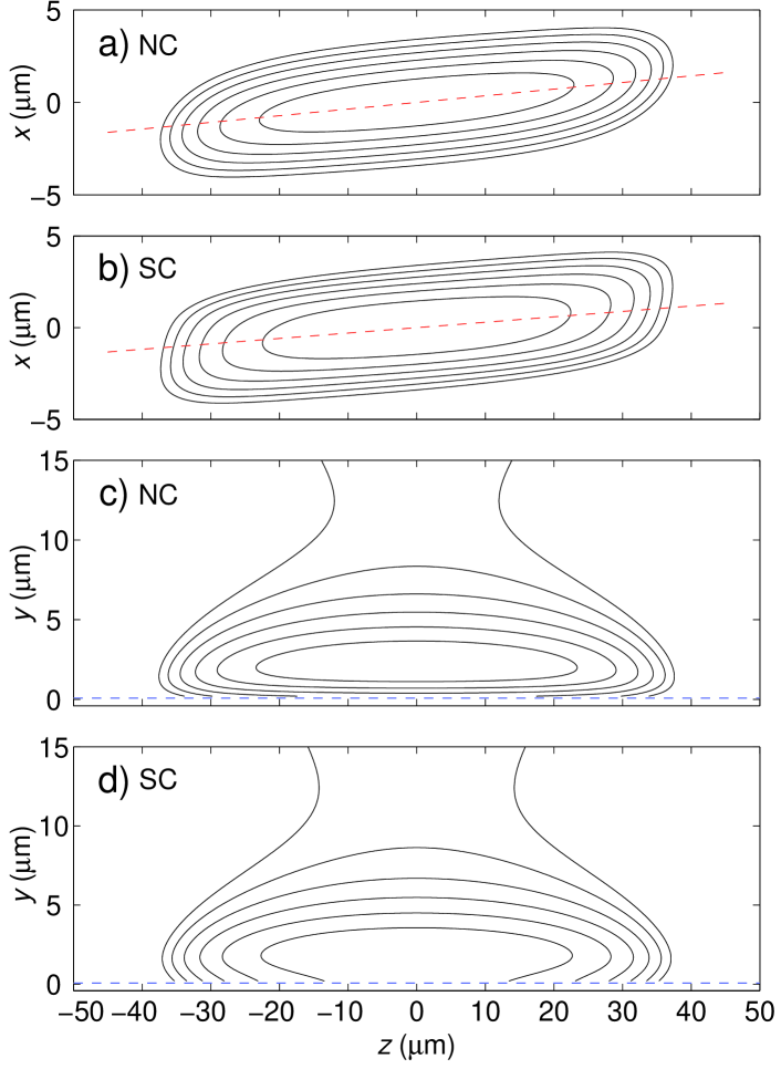
In this last section we apply the numerical results presented in Sec. IV to a typical example of a magnetic micro trap. Figure 11 shows the isopotential curves of a magnetic trap generated by the atom chip depicted in Fig. 1 in the superconducting and in the normal conducting state. The applied currents are the same in both cases. The relevant trap parameters are summarized in Table 1. The micro trap forms closer to the surface in the superconducting chip than in the normal conducting chip. In the present example, the Meissner effect produces an important reduction in the radial oscillation frequencies as well as a slight increase of the longitudinal oscillation frequencies, as predicted by Figs. 5 and 9.
The most remarkable feature of the supercoducting chip is a significant decrease of the trap depth towards the surface, which is a consequence of the reduction of shown in Fig. 5. In the shown example, the trap depth is reduced by about 80 in the superconducting chip.
| SC | NC | |
| (Tm-1) | 6.9 | 8.4 |
| (Tm-1) | 0.2 | 0.3 |
| (T) | 2.5 | 2.3 |
| (mTm-2) | 5700 | 5240 |
| (m) | 2.0 | 2.3 |
| (s-1) | 2 95 | 2 92 |
| (s-1) | 2 1650 | 2 2020 |
| 1.7∘ | 2.1∘ |
VI Conclusion
This theoretical study points out that differences between superconducting and normal conducting chips become relevant when the distance between the micro trap and the superconducting surface is smaller than the width of the wires. The most dramatic consequence of the Meissner effect is a significant reduction of the trap depth. In general, the Meissner effect has to be taken into account when designing and carrying out experiments with neutral atoms magnetically trapped near superconducting surfaces. Although the results shown in this paper have been obtained for the specific example illustrated in Fig. 1, these conclusions can be generalized to any atom chip made with superconducting thin films.
Acknowledgements.
This work was supported by the DFG (SFB TRR 21) and by the BMBF (NanoFutur 03X5506).References
- (1) J. Fortágh, and C. Zimmermann, Rev. Mod. Phys. 79, 235 (2007).
- (2) I. Teper, Y.-J. Lin, and V. Vuletic, Phys. Rev. Lett. 97, 023002 (2006).
- (3) Y. Colombe, T. Steinmetz, G. Dubois, F. Linke, D. Hunger, and J. Reichel, Nature 450, 272 (2007).
- (4) Y. -J. Wang, D. Z. Anderson, V. M. Bright, E. A. Cornell, Q. Diot, T. Kishimoto, M. Prentiss, R. A. Saravanan, S. R. Segal, and S. Wu, Phys. Rev. Lett. 94, 090405 (2005).
- (5) T. Schumm, S. Hofferberth, L. M. Andersson, S. Wildermuth, S. Groth, I. Bar-Joseph, J. Schmiedmayer, and P. Kruger, Nat. Phys. 1, 57 (2005).
- (6) G.-B. Jo, Y. Shin, S. Will, T. A. Pasquini, M. Saba, W. Ketterle, D. E. Pritchard, M. Vengalattore, and M. Prentiss, Phys. Rev. Lett. 98, 030407 (2007).
- (7) A. Günther, S. Kraft, C. Zimmermann, and J. Fortágh, Phys. Rev. Lett. 98, 140403 (2007).
- (8) J. Fortágh, H. Ott, S. Kraft, A. Günther, and C. Zimmermann, Phys. Rev. A 66, 041604(R) (2002).
- (9) S. Wildermuth, S. Hofferberth, I. Lesanovsky, E. Haller, L. M. Andersson, S. Groth, I. Bar-Joseph, P. Krüger, and J. Schmiedmayer, Nature 435, 440 (2005).
- (10) S. Du, M. B. Squires, Y. Imai, L. Czaia, R. A. Saravanan, V. M. Bright, J. Reichel, T. W. Hänsch, and D. Z. Anderson, Phys. Rev. A 70, 053606 (2004).
- (11) C. Henkel, S. Pötting, M. Wilkens, Applied Physics B 69, 379 (1999).
- (12) Y. J. Lin, I. Teper, C. Chin, and V. Vuletic, Phys. Rev. Lett. 92, 050404 (2004).
- (13) D. M. Harber, J. M. Obrecht, J. M. McGuirk, and E. A. Cornell, Phys. Rev. A 72, 033610 (2005).
- (14) M. P. A. Jones, C. J. Vale, D. Sahagun, B. V. Hall, and E. A. Hinds, Phys. Rev. Lett. 91, 080401 (2003).
- (15) P. K. Rekdal, S. Scheel, P. L. Knight, and E. A. Hinds, Phys. Rev. A 70, 013811 (2004).
- (16) U. Hohenester, A. Eiguren, S. Scheel, and E. A. Hinds, Phys. Rev. A 76, 033618 (2007).
- (17) P. Treutlein, D. Hunger, S. Camerer, T. W. Hänsch, and J. Reichel, Phys. Rev. Lett. 99, 140403 (2007).
- (18) M. Singh, arXiv:0709.0352v1 [quant-ph].
- (19) J. D. Weinstein and K. G. Libbrecht, Phys. Rev. A 52, 4004 (1995).
- (20) S. Scheel, P. K. Rekdal, P. L. Knight, and E. A. Hinds, Phys. Rev. A 72, 042901 (2005).
- (21) Bo-Sture K. Skagerstam, U. Hohenester, A. Eiguren, and P. K. Rekdal, Phys. Rev. Lett. 97, 070401 (2006).
- (22) F. London, Superfluids (Wiley, New York, 1950), Vol. I.
- (23) J. B. Ketterson, and S. N. Song, Superconductivity (Cambridge University Press,1999), Chap. 2.
- (24) C. Roux, A. Emmert, A. Lupascu, T. Nirrengarten, G. Nogues, M. Brune, J. -M. Raimond, and S. Haroche, arXiv:0801.3538v1 [physics.atom-ph].
- (25) T. Mukai, C. Hufnagel, A. Kasper, T. Meno, A. Tsukada, K. Semba, and F. Shimizu, Phys. Rev. Lett. 98, 260407 (2007).
- (26) E. H. Brandt, and G. P. Mikitik, Phys. Rev. Lett. 85, 4164 (2000).
- (27) M. M. Khapaev, Supercond. Sci. Technol. 9, 729 (1996).
- (28) E. Pardo, A. Sanchez, and C. Navau, Phys. Rev. B 67, 104517 (2003).
- (29) A. Günther, M. Kemmler, S. Kraft, C. J. Vale, C. Zimmermann, and J. Fortágh, Phys. Rev. A 71, 063619 (2005).
- (30) C. V. Sukumar, and D. M. Brink, Phys. Rev. A 56, 2451 (1997).
- (31) R. I. Joseph, and E. Schlömann, J. Appl. Phys. 36, 1579 (1965).
- (32) F. W. Grover, Inductance Calculations (D. Van Nostrand Company, Inc., New York,1946), Chap. 2&5.
- (33) R. Meservey, and P. M. Tedrow, J.Appl.Phys. 40, 2028 (1969).
- (34) It has been numerically solved in Mathematica using the function NIntegrate.
- (35) The energy and flux can be properly evaluated from the closed current elements when these occupy the whole volume of the superconducting body and when the overlapping between neighbor current elements is total, in the sense that a homogeneous distribution of closed current elements generate null electric current at any internal point that is not on the surface of the superconducting body.