Enhanced tunneling magnetoresistance in FeZnSe double junctions
Abstract
We calculate the tunneling magnetoresistance (TMR) of FeZnSeFeZnSeFe (001) double magnetic tunnel junctions as a function of the in-between Fe layer’s thickness, and compare these results with those of FeZnSeFe simple junctions. The electronic band structures are modeled by a parametrized tight-binding Hamiltonian fitted to ab initio calculations, and the conductance is calculated within the Landauer formalism expressed in terms of Green’s functions. We find that the conductances for each spin channel and the TMR strongly depend on the in-between Fe layer’s thickness, and that in some cases they are enhanced with respect to simple junctions, in qualitative agreement with recent experimental studies performed on similar systems. By using a 2D double junction as a simplified system, we show that the conductance enhancement can be explained in terms of the junctions energy spectrum. These results are relevant for spintronics because they demonstrate that the TMR in double junctions can be tuned and enhanced by varying the in-between metallic layer’s thickness.
pacs:
85.75.-d, 72.25.Mk, 73.40.Rw, 73.23.AdA magnetic tunnel junction (MTJ) consists of two ferromagnetic electrodes separated by a thin non-conducting barrier. It is experimentally observed that the conductance of a MTJ depends on the relative orientation of the electrodes’ magnetization, and because of this, during the last years a lot of attention has been paid to the investigation of MTJs as promising candidates for application in spintronic devices, such as read heads and magnetic random access memories (for reviews, see [1] and the references therein).
One of the challenges, that has to be overcome for practical applications, is to reach higher values of the tunneling magnetoresistance ratio (TMR), defined as TMR, where and are the conductances measured for the parallel (P) and antiparallel (AP) magnetization of the electrodes. Several possibilities are now being considered: to use highly polarized materials (half-metals) or diluted magnetic semiconductors as parts of MTJs, to produce junctions with almost perfect interfaces, and to use double magnetic tunnel junctions (DMTJs), in which metallic layers are inserted inside the semiconductor barrier of a MTJ. In this work we explore the latter alternative, and focus our attention on the dependence of the TMR on the in-between metallic layer’s thickness.
Since X. Zhang et al [2] suggested to use DMTJs, several groups [3-6] have theoretically shown that DMTJs exhibit richer spin-dependent transport properties than MTJs and that the TMR can be higher than that of MTJs, but only very recently could these DMTJs be fabricated [7,8]. T. Nozaki et al [7] have recently measured the tunnel magnetoresistance of epitaxial FeMgOFeMgOFe (001) DMTJs at room temperature, and found an enhancement of the TMR with respect to MTJs (53 for DMTJs versus 44 for MTJs at low bias), indicating that DMTJs may present an advantage over simple junctions for their use in spintronics.
As far as we know, up to now the only theoretical studies of DMTJs with magnetic layers in between the semiconductor were made within the free electron model (that cannot reproduce the decay rates inside the semiconductor of evanescent states with different symmetry), and using rectangular potential profiles [2,3,5,14]. Moreover, these studies analyzed the dependence of TMR on the applied bias voltage and not on the in-between metallic layer’s thickness, as we do in this work. For this reason, in this paper transport through Fe()ZnSe()Fe() (001) MTJs and through Fe()ZnSe()Fe()ZnSe()Fe() (001) DMTJs is theoretically investigated using a realistic tight-binding (TB) Hamiltonian to obtain the electronic structure of the junctions. Fe() are semi-infinite electrodes, and , and denote thicknesses. The systems studied are epitaxial, and we restrict to zero temperature, infinitesimal bias voltage and elastic transport. We choose FeZnSe because it can be grown epitaxially and there is very little interdiffusion at the interfaces, thus producing crystalline junctions in which there are no magnetically dead Fe layers [9,10]. Moreover, in contrast to what happens in FeMgO based junctions, there is no oxidation of the interfacial Fe layers, which is known to be detrimental to TMR [11]. To obtain a clearer insight into the physics involved in transport through double tunnel junctions, we also calculate the conductance through a simplified two-dimensional tunnel junction (2DDJ).
The conductances are calculated from the active region’s Green’s function , where stands for the unit matrix, is the Hamiltonian corresponding to the active region, are the self-energies describing the interaction of the active region with the left (L) or right (R) electrodes ( corresponds to the majority or minority spin channels), and ’active region’ stands for whatever is sandwiched by the electrodes. For DMTJs, the active region consists of an ’in-between metal region’ (IBMR) sandwiched by two identical ’semiconductor regions’ (SCR), while for MTJs the active region is simply the SCR. The energy is actually , being the Fermi level of the system, and we take . The self-energies are given by and , where and describe the coupling of the active region with the electrodes, and are the surface Green’s functions for each electrode. These surface Green’s functions are calculated using a semi-analytical method [12] and are exact within our TB approximation. The transmission probability is given by [13] where , while the conductance is given by
| (1) |
where is the total number of wave vectors parallel to the interface that we consider (in our case 5000 is enough to achieve convergence in ).
We start our discussion with the 2DDJs case, which are of the type M()SMSM(), where M() are semi-infinite paramagnetic metallic electrodes, S is a semiconductor and M is a metal (the same as the electrodes). The metal and semiconductor have the same structure, a square Bravais lattice with two atoms per unit cell, and are periodic in the direction perpendicular to the transport direction. The 2DDJs electronic structure is modeled by a 2nd nearest neighbors TB Hamiltonian with one orbital per atom. The TB parameters are chosen to make fall in the middle of the semiconductor’s band gap (of 0.5 eV). The SC and IBM regions are varied between 3.2 Å and 32 Å .
It is found that for certain thicknesses of the IBMR the conductance presents peaks in which it is enhanced by 1 to 4 orders of magnitude, as can be seen in Fig. 1 for a 2DDJ with a SCR of 12.8 Å . This effect can be explained in terms of the active region’s density of states (DOS), obtained from its Green’s function . When the conductance is enhanced, partial density of states (PDOS) calculations indicate that there exist states at extended throughout the whole junction, so in that situations transport occurs through resonant states. When this happens, the 2DDJs conductances are higher than the corresponding ones of simple 2D junctions. These results are consistent with those of Z. Zheng and coworkers for a DMTJ with a non-magnetic in-between metal [14].
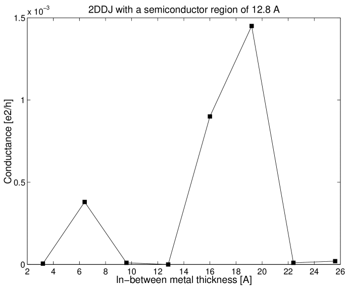
Fig. 2 shows the maximum ratio between the conductance of 2DDJs and 2D simple junctions, as a function of the SCR thickness. The maximum attainable ratio is of 146 and occurs for a SCR thickness of 9.6 Å and an IBMR thickness of 19.2 Å . For thinner SCRs the ratio is nearly constant and roughly 140 , but beyond 12.8 Å the enhancement effect is lost. Having mentioned the main results for the 2DDJs, we go on to discuss the details for the three-dimensional FeZnSe DMTJs.
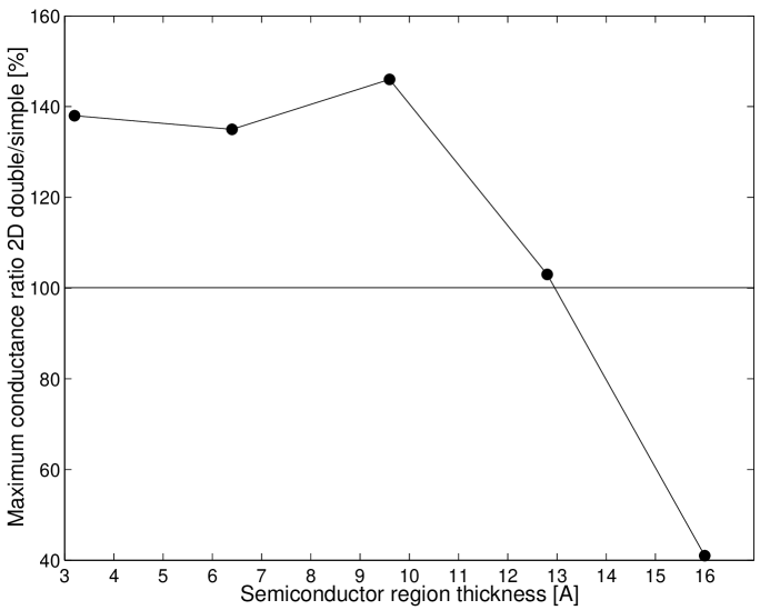
Fig. 3 shows schematically the structure of simple and double junctions, which are periodic in the x-y plane, and the different magnetic configurations considered, parallel (P) and antiparallel (AP). Since the coercive field of the electrode and the in-between Fe layers is different, the magnetic configurations shown are experimentally attainable [7].
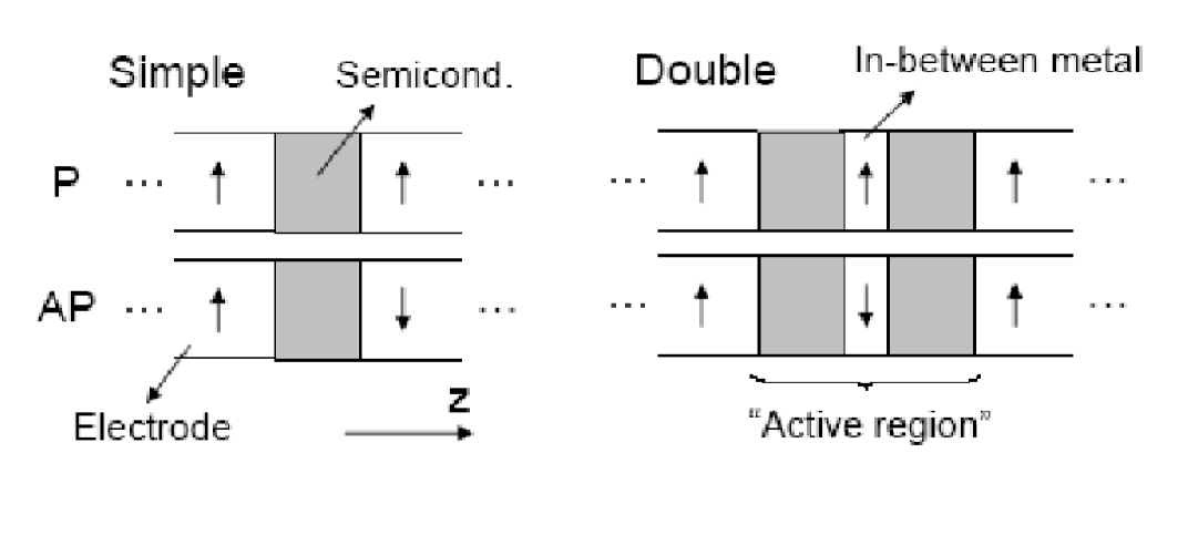
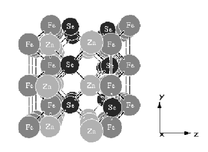
Fig. 4 shows the structure of a simple FeZnSe junction with a SCR of 5.67 Å , along the direction (which is the direction of transport). The BCC Fe lattice parameter is Å , and that of zincblende ZnSe is Å .
The electronic structure of the junctions is modeled by a parametrized 2nd nearest neighbors spd TB Hamiltonian fitted to ab initio calculations [15,16], in which the hoppings between the Fe atoms and the (Zn,Se) atoms are calculated using Shiba’s rules and Andersen’s scaling law [17]. The Fe bands are spin split by , where is the experimental magnetic moment of Fe and eV is the exchange integral between orbitals ( is Bohr’s magneton). With these values for and , the Fe bands spin spitting is very well reproduced [15]. The ZnSe band structure is rigidly shifted to make the iron Fermi energy fall 1 eV above the ZnSe valence band and 1.1 eV below the conduction band, as indicated by photoemission experiments [9].
For simple junctions, we find that the conductances decay almost exponentially with semiconductor thickness, and that the TMR increases and is always positive (or direct), reaching a value of 90 for a semiconductor thickness of 34 Å . Our results are in very good agreement with the ab initio results of MacLaren and coworkers [18].
For double junctions, we vary the SCR thickness between 5.67 Å and 28.35 Å , and the IBMR thickness between 2.87 Å and 22.96 Å . We find that the TMR and conductances strongly depend on the in-between metal thickness, and that for certain thickness combinations of the SC and IBM regions they can be higher than those corresponding to a MTJ, in agreement with the results of L. Sheng and coworkers [3]. The maximum ratio of DMTJs to simple MTJs conductances obtained is of 322 , and occurs for the P majority channel corresponding to SC regions of 22.7 Å and an IBM region of 21 Å . This large conductance ratio, which is pointing toward the existence of resonant states (confirmed by our DOS calculations), does not mean that the DMTJs TMR is going to be much larger than the MTJs one, although in general it is. In this particular case, the TMR value is of 97.9 (the corresponding MTJ’s value is 63.8 ), but in other cases the TMR values are greatly enhanced even in the absence of resonances. We find that the TMR enhancement can be a result of: (i) a drop in the conductance of some spin channels, while the conductances of other channels remain of the same order of magnitude as those in MTJs, or (ii) an increase in the conductance of one particular spin channel due to resonant tunneling. Both effects are produced by a change in the active region’s DOS near , induced by the presence of the in-between Fe layers.
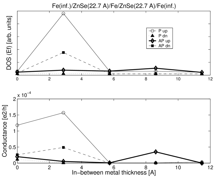
As an example of resonance conductance enhancement, we show in Fig. 5 the active region’s total DOS at , as a function of the IBMR thickness and for a DMTJ with a SCR of 22.7 Å . An increase in one order of magnitude appears at an IBMR of 2.87 Å for the P majority channel and for the AP minority channel, and a smaller increase appears at an IBMR of 8.6 Å for the AP majority channel, while for the other cases the DOS is almost constant. These peaks coincide with a conductance enhancement in these three channels, as it can be seen in the lower panel of Fig. 5, indicating that the origin of the conductance enhancement is the same as in 2DDJs, namely resonant tunneling.
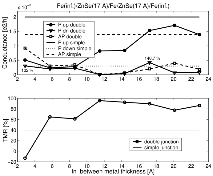
To visualize the interplay among the conductance values of the different channels and configurations, Fig. 6 shows the conductances and TMR values for a given DMTJ with a SCR of 17 Å and those of the corresponding simple MTJ, as a function of the IBMR thickness. It is seen that, already for 6 Å of Fe, the TMR is 1.5 times higher than that of a simple MTJ, although the conductances are, in general, a little bit smaller. This is similar to what happens in all the cases studied. It is noticeable that for very thin Fe layers the TMR obtained for this DMTJ is negative, and that for IBMR thicknesses in the range 12-23 Å the TMR is almost constant. This also happens for the other SCR thicknesses studied, and it is different to the damped oscillatory behavior that it is obtained using rectangular potential profiles and a non-magnetic in-between metal [4].
For a given SC region thickness, we look for the maximum attainable TMR value by sweeping over IBMR’s thicknesses. We find that for ZnSe regions with thicknesses below 20 Å , the DMTJs’ TMR values are 3 times higher than those of a simple junction, while the conductances of some spin channels remain of the same order of magnitude. Beyond this thickness, the DMTJs TMR can be 50 times higher but negative (inverse TMR), although in this case the conductances of all spin channels are 4 to 6 orders of magnitude smaller, and thus very hard to measure. There is one particular case in which this does not happen. For a DMTJ with a SCR of 22.7 Å and an IBMR of 8.6 Å , we obtain a drop in the conductances of the P and AP minority channels and the P majority channel, and an enhancement of 175 in the AP majority channel with respect to the corresponding MTJ, which results in a negative TMR enhancement by a factor of -40.
In summary, we have investigated FeZnSe double magnetic tunnel junctions within a realistic Hamiltonian model and found that the TMR values can be much higher than those of simple junctions. We should mention that temperature effects, interfacial roughness, and the presence of defects in the DMTJs active region may decrease the TMR values obtained in our calculations, but we believe that our results remain qualitatively valid. We conclude that the thickness of the in-between Fe layers in FeZnSe DMTJs is an interesting degree of freedom, which may make it possible to tune and enhance the TMR of these systems, making them suitable for building future spintronic devices. To improve our understanding of these scarcely studied double junctions, it is highly desirable the experimental measurement of the TMR as a function of the in-between metallic layers thickness.
We are grateful to Julián Milano for useful discussions. This work was partially funded by UBACyT-X115, Fundación Antorchas and PICT 03-10698. Ana María Llois belongs to CONICET (Argentina).
X-G. Zhang and W. H. Butler, J. Phys.: Condens. Matter 15, 1603
(2003); E. Y. Tsymbal, O. N. Mryasov, and P. R. LeClair
ibid. 15, 109 (2003)
X. Zhang, B-Z Li, G. Sun, and F-C. Pu, Phys. Rev. B
56, 5484 (1997)
L. Sheng, Y. Chen, H. Y. Teng, and C. S. Ting, Phys. Rev. B 59,
480 (1999)
M. Chshiev, D. Stoeffler, A. Vedyayev, and K. Ounadjela, Europhys. Lett.
58, 257 (2002)
B. Wang, Y. Guo, and B-L. Gu, J. Appl. Phys. 91, 1318 (2002)
F. Giazotto, Fabio Taddei, Rosario Fazio, and Fabio Beltram, Appl. Phys. Lett.
82, 2449 (2003)
T. Nozaki et al, Appl. Phys. Lett. 86, 082501 (2005)
Z. Zeng et al, Phys. Rev. B 72, 054419 (2005);
J. H. Lee et al, J. Magn. Magn. Mater. 286,
138 (2005)
M. Eddrief et al, Appl. Phys. Lett. 81, 4553 (2002)
M. Marangolo et al, Phys. Rev. Lett. 88,
217202-1 (2002)
X-G. Zhang, W. H. Butler, and A. Bandyopadhyay,
Phys. Rev. B 68, 092402 (2003)
S. Sanvito et al, Phys. Rev. B 59,
11936 (1999)
S. Datta, ’Electronic transport in mesoscopic systems’
(Cambridge University Press, United Kingdom, 1999)
Z. Zheng, Y. Qi, D. Y. Xing, and J. Dong, Phys. Rev. B 59, 14505
(1999)
D. A. Papaconstantopoulos, ’Handbook of the band structure of
elemental solids’ (Plenum Press, New York, 1986)
R. Viswanatha, S. Sapra, T. Saha-Dasgupta and D. D. Sarma,
cond-mat 0505451 v1, 18 May 2005
O. K. Andersen, Physica B 91, 317 (1977)
J. M. MacLaren, X. G. Zhang, W. H. Butler and X. Wang,
Phys. Rev. B 59, 5470 (1999)