Bias-controlled sensitivity of ferromagnet/semiconductor electrical spin detectors
Abstract
Using Fe/GaAs Schottky tunnel barriers as electrical spin detectors, we show that the magnitude and sign of their spin-detection sensitivities can be widely tuned with the voltage bias applied across the Fe/GaAs interface. Experiments and theory establish that this tunability derives not just simply from the bias dependence of the tunneling conductances (a property of the interface), but also from the bias dependence of electric fields in the semiconductor which can dramatically enhance or suppress spin-detection sensitivities. Electrons in GaAs with fixed polarization can therefore be made to induce either positive or negative voltage changes at spin detectors, and some detector sensitivities can be enhanced over ten-fold compared to the usual case of zero-bias spin detection.
An all-electrical scheme for efficient detection of spins is an essential component of most “semiconductor spintronic” device proposals Zutic ; Jansen , and recent demonstrations of electrical spin injection and detection in GaAs Johnson2 ; Bhatta ; LouNP , silicon Huang ; vantErve , and graphene Tombros have motivated a desire to understand how bulk and interfacial spin transport contribute to device performance. However, while the need for optimizing spin injection is widely recognized, the interplay of mechanisms that govern electrical spin detection have only begun to be explored Jansen ; Bhatta ; Fert .
Recent progress on spin-transport devices with semiconductor channels has relied on spin-dependent electron tunneling through barriers formed at ferromagnet-semiconductor interfaces MJcomment ; Rashba ; Smith . However, tunneling typically introduces a strong and often unpredictable dependence of the tunneling current polarization, , on interface voltage bias. For example, tunneling magnetoresistances through vertical Fe/GaAs/Fe trilayers were found to invert sign when one interface was epitaxial Moser . In lateral Fe/GaAs devices, varied markedly with source electrode bias, unexpectedly inverting sign under forward bias in some structures and under reverse bias in others LouNP . Accordingly, several recent theories have attempted to understand spin tunneling through ferromagnet-semiconductor interfaces DeryPRL ; ChantisPRL ; Fert . In addressing the relevance of these models to the equally-important problem of spin detection, there is a critical and largely unexplored need to separate interfacial tunneling effects from the effects of spin transport due to electric fields YuFlatte ; Schmidt in the semiconductor.
Here we use lateral Fe/GaAs structures to study the influence of a detector interface bias () on the sensitivity of electrical spin detection, which we define as the voltage change induced by an additional, remotely-injected spin polarization. Crucially, we show that spin-detection sensitivities cannot be understood from the detector interface’s tunneling properties () alone. Instead, both experiments and theory show that can be significantly enhanced or suppressed compared to – in a controlled and predictable fashion – due to the resulting electric fields in the semiconductor, which modify the spin densities () and their gradients at biased Fe/GaAs detector interfaces. These new phenomena cannot occur in conventional non-local studies that use spin detectors operating at zero bias, nor are they expected in all-metal devices having large channel conductivities and therefore negligible electric fields.
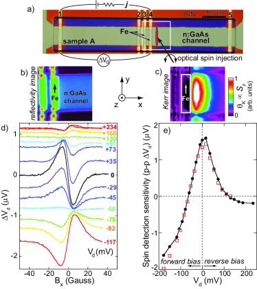
Fig. 1(a) shows a typical device. Epitaxial Fe/GaAs structures are processed into lateral spin-transport devices having five 1050 m Fe contacts (#1-5) on a 2.5 m thick n-type GaAs channel LouNP . A Schottky tunnel barrier is formed at the interface between Fe and a highly-doped interfacial layer of GaAs Hanbicki . Devices from two wafers are discussed (denoted A and B, with =3.5 and 2.01016 cm-3); these represent structures for which inverts under finite forward and reverse source bias, respectively LouNP .
To measure the spin-detection sensitivity of these Fe/GaAs electrodes in a background-free manner, we employ an optical pumping technique. First, a constant current establishes a voltage drop across a Fe/GaAs detector interface (contact #4 in Fig. 1). From Smith ,
| (1) |
where is the tunneling current polarization, and and are the majority- and minority-spin tunneling currents and conductances. A weak, circularly-polarized, 1.58 eV pump laser is then focused to a stripe 10-20 m away from contact 4, injecting a small constant spin polarization in the channel. This additional polarization, oriented initially along , drifts and diffuses laterally and is tipped into the minority or majority spin direction with respect to the Fe magnetization M () by small applied fields . At the Fe/GaAs detector interface, this polarization modifies the chemical potentials which (at constant ) necessarily modifies and therefore changes by an amount that is a direct measure of the detector’s spin sensitivity. The dependence of on derives both from the bias dependence of (a property of the interface), and from the optically-induced changes to (which depend on electric fields in the GaAs, as detailed later).
To explicitly measure spin-dependent changes, the laser is modulated from right- to left-circular polarization at 50 kHz, and at this frequency is measured between the detector and a distant reference contact. Importantly, this approach avoids magnetic dichroism and hot electron artifacts because spins are injected into the channel (rather than through the Fe contact), where they cool before diffusing. Using scanning Kerr-rotation microscopy Stephens ; CrookerScience ; FurisNJP ; Kotissek , Figs. 1(b,c) show images of the reflectivity, and of the optically-injected polarization diffusing to the right and also to the left towards the spin detector. Using low laser power (10 W), perturbations to are intentionally kept small, of order 1 V.
Fig. 1(d) shows versus at different biases across the Fe/GaAs detector. Effectively, we electrically detect the component of diffusing and precessing spins that are optically oriented initially along . Thus, the data show antisymmetric “local Hanle” lineshapes that depend on spin lifetimes, diffusion constants, and source/detector separation CrookerScience ; FurisNJP . Maximum and minimum occur at for which the injected spins precess on average (M) upon reaching the detector. Larger causes rapid ensemble dephasing.
The peak-to-peak amplitudes of these curves [Fig. 1(e)] therefore provide a relative measure of the electrical spin-detection sensitivity that depends only on the spin-dependent voltages induced by the remotely-injected spins. In sample A, is clearly tunable with detector bias. It is large and positive near =0, where the remotely-injected spins induce a positive (+1.5 V) at the detection electrode. With increasing forward or reverse detector bias, however, decreases and inverts sign – now, these same spins induce a negative voltage change. Electrons in GaAs with fixed spin can therefore be made to generate positive or negative voltage changes at these Fe/GaAs spin detectors by tuning by a few tens of mV, offering new routes (besides manipulating electron spins or contact magnetizations) to tune and switch spin-dependent electrical signals.
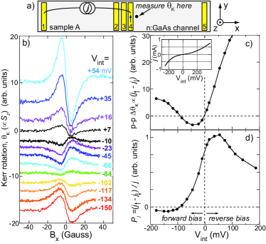
To understand this tunable spin detection sensitivity, it is essential to independently measure , the polarization of the tunneling current that flows across this biased Fe/GaAs interface. For this we measure the electrical spin injection efficiency of this electrode using Kerr-rotation methods, as demonstrated previously LouNP . Here (see Fig. 2), a probe laser detects the -component of electrically-injected spins via the Hanle-Kerr effect, versus , at a point 10 m to the right of contact #4. These curves exhibit similar “local Hanle” lineshapes as seen in Fig. 1(d). Extrema occur at for which the spins have on average precessed 90∘ (from to ) at the detection point. A series of curves are shown in Fig. 2(b) at various interface biases, , across contact 4. Their peak-to-peak amplitude is proportional to the difference between injected majority- and minority-spin densities, which necessarily scales directly with the difference between majority- and minority-spin tunneling currents: . Fig. 2(c) shows and the current-voltage trace for contact 4. Normalizing by the total current reveals the relative polarization of the interface tunneling current, [see Fig. 2(d)]. depends strongly on , showing a maximum (majority spin) polarization near +50 mV, and a sign inversion at -90 mV forward bias. All contacts on sample A and on other devices from this wafer show the same bias dependence of .
Comparing sample A’s spin-detection sensitivity with [Figs. 1(e) and 2(d)], general trends can now be identified: Both exhibit a positive maximum near zero bias, and the inversion of under small forward bias can now be understood by the similar inversion of . However, a key finding is that striking differences exist at large interface bias: Compared to , is markedly enhanced under large forward bias, but is suppressed under large reverse bias ( also inverts sign again at +130 mV, which is unexpected and does not follow from ). Thus, spin-detection sensitivities in these Fe/GaAs structures do not simply track as might be expected from reciprocity arguments, and their strong deviation at larger biases suggests the important and nontrivial role of electric fields in the GaAs, discussed below.
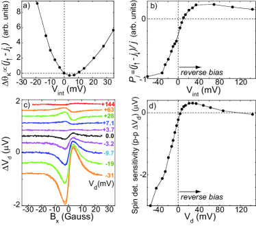
Fig. 3 shows corroborating data from sample B. In contrast to sample A, injection studies [Figs. 3(a,b)] show that is now dominated by minority spins at zero bias and that now inverts at finite reverse bias (+10 mV). These differences likely originate in the microscopic details of this Fe/GaAs interface, which are not yet fully understood DeryPRL ; ChantisPRL . Nonetheless, the sensitivity of sample B’s spin detectors [Figs. 3(c,d)] can be correlated with . At zero bias, the remotely injected spins now generate small negative voltage changes at detection electrodes (-0.2 V), which now invert sign at small reverse detector bias, similar to . However, like sample A, diverges markedly from at large bias: is suppressed at large reverse bias, but is greatly enhanced – over tenfold – with only -40 mV forward bias, transforming a poor zero-bias spin detector into a much more sensitive spin detection device.
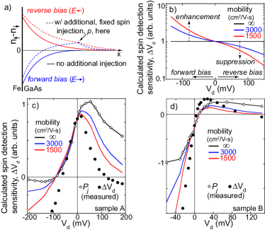
The enhancement and suppression of can be understood within a 1-D model of spin transport in the semiconductor and its non-trivial influence on spin detection Athanasios . As Fig. 4(a) depicts, a unit polarization generated in the channel modifies the spin density difference and its gradient at a nearby Fe/GaAs detector interface (in the figure, both increase). At a fixed interface current , these modifications necessarily change if . From Eq. (1), one can derive the induced change in detector voltage: = , where =, and are the electron diffusion constant and mobility, is the electric field in the semiconductor, and and its gradient are evaluated at the interface. Using the spin transport model of Smith and the full spin-drift-diffusion equations, one finds Athanasios that can deviate markedly from because: i) trivially, can drift away from (towards) the detector in reverse (forward) bias, while ii) at the interface itself, the diffusion and drift terms oppose each other in reverse bias (0) but add in forward bias (0). The importance of (ii) is clearly seen in Fig. 1(e), where nearly identical detection sensitivities are measured even when is injected in the current path. Note that 10 V/cm – rather modest – in these studies.
These enhancement and suppression effects are normally superimposed on the bias dependence of , but are disentangled in Fig. 4(b) by showing calculated for an idealized (constant) . Crucially, detection sensitivities are enhanced or suppressed relative to due to , which depends sensitively on the channel conductivity. For “metallic-like” channels, tracks exactly, because 0. Notably, this model suggests that can also be controlled (independent of ) by engineering the conductivity of semiconductor devices.
We explicitly calculate for samples A and B using determined from experimental and data. Electron densities and spin lifetimes are measured independently. The results [Figs. 4(c,d)] are scaled so that at zero bias. For realistic n:GaAs mobilities, the calculated drops (increases) much more rapidly than under large reverse (forward) bias, in good overall agreement with measured values. (The inversion of at large reverse bias is not reproduced in this 1-D model because drift and diffusion terms cancel exactly, suppressing monotonically to zero Athanasios . No such restriction exists in 2-D or 3-D geometries, which permit inhomogeneous fields.)
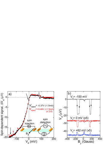
Finally, these results suggest that it should be possible to tune and enhance the detection of electrically-injected spins. This is demonstrated in Fig. 5, where non-local lateral spin-valve studies LouNP were performed on a device having similar to sample B. Fig. 5(a) shows the spin-valve signal versus detector bias, when the source electrode is forward- or reverse-biased. The dependence on is the same, confirming that a detector’s sensitivity can be optimized independently of an injector’s biasing. Fig. 5(b) shows raw spin-valve data with =-150, 0, and +82 mV, explicitly showing that spin-detection sensitivities are freely tunable in both sign and magnitude in all-electrical devices.
In these studies, both interfacial biases and electric fields play essential roles. Because semiconductors can support large electric fields, it is possible to bias each element – source, channel, and detector – independently in multiterminal devices. Controlling spin transport through both interfacial and bulk band structures represents a unique capability of ferromagnet-semiconductor devices that is only beginning to be explored. The authors acknowledge support from the Los Alamos LDRD program, ONR, NSF MRSEC, NNIN and IGERT programs.
References
- (1) I. Žutić, J. Fabian, and S. Das Sarma, Rev. Mod. Phys. 76, 323 (2004).
- (2) R. Jansen and B. C. Min, Phys. Rev. Lett. 99, 246604 (2007).
- (3) P. R. Hammar and M. Johnson, Phys. Rev. Lett. 88, 066806 (2002).
- (4) D. Saha, M. Holub, and P. Bhattacharya, Appl. Phys. Lett. 91, 072513 (2007).
- (5) X. Lou, C. Adelmann, S. A. Crooker, E. S. Garlid, J. Zhang, K. S. M. Reddy, S. D. Flexner, C. J. Palmstrøm, and P. A. Crowell, Nat. Phys. 3, 197 (2007).
- (6) I. Appelbaum, B. Huang, and D. J. Monsma, Nature 447, 295 (2007).
- (7) O. M. J. van ’t Erve, A. T. Hanbicki, M. Holub, C. H. Li, C. Awo-Affouda, P. E. Thompson, and B. T. Jonker, Appl. Phys. Lett. 91, 212109 (2007).
- (8) N. Tombros, C. Jozsa, M. Popinciuc, H. T. Jonkman, and B. J. van Wees, Nature 448, 571 (2007).
- (9) M. Tran, H. Jaffrès, C. Deranlot, J.-M. George, A. Fert, A. Miard, and A. Lemaître, Phys. Rev. Lett. 102, 036601 (2009).
- (10) M. Johnson and R. H. Silsbee, Phys. Rev. Lett. 60, 377 (1988).
- (11) E. I. Rashba, Phys. Rev. B 62, R16267 (2000)
- (12) D. L. Smith and R. N. Silver, Phys. Rev. B 64,045323 (2001).
- (13) J. Moser, M. Zenger, C. Gerl, D. Schuh, R. Meier, P. Chen, G. Bayreuther, W. Wegscheider, D. Weiss, C.-H Lai, R.-T Huang, M. Kosuth, and H. Ebert, Appl. Phys. Lett. 89, 162106 (2006).
- (14) H. Dery and L. J. Sham, Phys. Rev. Lett. 98, 046602 (2007).
- (15) A. N. Chantis, K. D. Belashchenko, D. L. Smith, E. Y. Tsymbal, M. van Schilfgaarde, and R. C. Albers, Phys. Rev. Lett. 99, 196603 (2007).
- (16) Z. G. Yu and M. E. Flatté, Phys. Rev. B 66, 201202(R) (2002).
- (17) G. Schmidt, C. Gould, P. Grabs, A. M. Lunde, G. Richter, A. Slobodskyy, and L. W. Molenkamp, Phys. Rev. Lett. 92, 226602 (2004).
- (18) A. T. Hanbicki, O. M. J. van ’t Erve, R. Magno, G. Kioseoglou, C. H. Li, B. T. Jonker, G. Itskos, R. Mallory, M. Yasar, and A. Petrou, Appl. Phys. Lett. 82, 4092 (2003).
- (19) J. Stephens, J. Berezovsky, J. P. McGuire, L. J. Sham, A. C. Gossard, and D. D. Awschalom, Phys. Rev. Lett. 93, 097602 (2004).
- (20) S. A. Crooker, M. Furis, X. Lou, C. Adelmann, D. L. Smith, C. J. Palmstrøm, and P. A. Crowell, Science 309, 2191 (2005).
- (21) M. Furis, D. L. Smith, S. Kos, E. S. Garlid, K. S. M. Reddy, C. J. Palmstrøm, P. A. Crowell, and S. A. Crooker, New J. Phys. 9, 347 (2007).
- (22) P. Kotissek, M. Bailleul, M. Sperl, A. Spitzer, D. Schuh, W. Wegscheider, C. H. Back, and G. Bayreuther, Nat. Phys. 3, 872 (2007).
- (23) A. N. Chantis and D. L. Smith, Phys. Rev. B 78, 235317 (2008).