Kondo effects in a single-molecule transistor.
Abstract
We have used the electromigration technique to fabricate a single-molecule transistor (SMT). We present a full experimental study as a function of temperature, down to 35 mK, and as a function of magnetic field up to 8 T in a SMT with odd number of electrons, where the usual spin-1/2 Kondo effect occurs, with good agreement with theory. In the case of even number of electrons, a low temperature magneto-transport study is provided, which demonstrates a Zeeman splitting of the zero-bias anomaly at energies well below the Kondo scale.
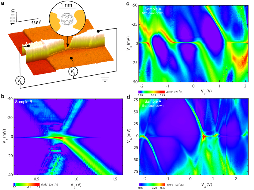
A single-molecule transistor is the smallest three terminal electronic devices, consisting of two electrodes (source and drain) and a gate, as shown on Fig.1a. Due to nanometric confinement of the wave-function of the electrons in a SMT, Coulomb blockade phenomena are expected McEuen2000 ; Ralph2002 ; Ward2008 ; Liang2002bis ; Kubatkin2003 ; Champagne2005 . Depending on the voltage bias and the gate voltage , the transistor can be tuned to allow current flowing or not through the single-molecule, resulting in Coulomb diamond diagrams (Fig.1b,c,d). The number of observed Coulomb diamonds in an experiment strongly depends on the molecule-to-gate coupling as well as on the charging energy of the SMT. However, the molecular level spacing and the charging energy extracted from the SMT measurements are perturbated compared to those of a molecule in solution, leading to a decrease of the addition energy . As a result, this latter quantity strongly depends on the coupling to the reservoirs Kubatkin2003 , as well on its redox state. For example, is expected to be of the order of eV when we consider the HOMO-LUMO gap of , but can be much lower Elste2005 if we consider intra fivefold-degenerate HOMO or threefold-degenerate LUMO transitions ( meV).
Focusing on an odd number of electrons in a SMT, when a spin-1/2 magnetic impurity in the quantum dot (QD) is strongly coupled antiferromagnetically to the electrons in the reservoirs, the electronic states of the QD hybridize with the electronic states of the reservoirs. As a result, even if the energy of the QD state is far below the Fermi level of the reservoirs, hybridization creates an effective density of states on the site of the dot, which is pinned to the Fermi level of the reservoirs, leading to a zero-bias conductance anomaly where a Coulomb gap would have naively been expected. This is known as the Kondo effect in QD devices Glazman1988 ; Ng1988 , and this signature has been widely observed in semiconducting devices Goldhaber1998 ; Cronenwett1998 , carbon nanotubes Nygard2000 or single-molecule QDs Liang2002bis ; Yu2004 . Universality is a fundamental property of the Kondo effect and a single energy scale, associated with the Kondo temperature , fully describes the physical properties at low energy. When the typical energy of a perturbation, such as temperature, bias voltage, or magnetic field, is higher than , the coherence of the system is suppressed and the Kondo effect disappears.
We report here on a full experimental study of the spin-1/2 Kondo effect in a single molecule embedded in a nanoconstriction fabricated by means of electromigration. The spin-1/2 Kondo effect in a molecular junction was observed for the first time by Yu and Natelson Yu2004 (see also Pasupathy2004 in the case of ferromagnetic electrodes), and more recently by Parks et al. Parks2007 using mechanically controllable break junctions. However, to our knowledge, no electromigration procedure has been carried out in a dilution refrigerator with a high degree of filtering. Improvements of the original procedure Park1999 have already been reported recently Strachan2005 ; Esen2005 ; Trouwborst2006 ; O'Neill2007 ; Wu2007 . The creation of nanogaps with this technique requires minimizing the series resistance vanderZant2006 ; Taychatanapat2007 , which is generally incompatible with dilution refrigerator wiring and filtering. To overcome this problem, we developed a specific measurement setup described in the supplementary information of reference Roch2008 . Another disadvantage encountered during the electromigration process, when the molecule under investigation is deposited before the realization of the nano-gap, is local heating of the nano-wire up to approximately K Trouwborst2006 ; Lambert2003 . We have then chosen to realize our SMT using molecules, because fullerenes can easily undergo such annealing.
Preparation of the SMT was realized by blow drying a dilute solution of a molecules in toluene onto a gold nano-wire realized on an back gate (see Fig. 1a for a schematic view of the setup). Before blow drying the solution, the electrodes were cleaned with acetone, ethanol, isopropanol and an oxygen plasma. The connected sample is inserted into a copper shielded box, enclosed in a high frequency low-temperature filter, which is anchored to the mixing chamber of the dilution refrigerator. The nano-wire coated with molecules is then broken by electromigration Park1999 , via a voltage ramp at K. However, it is difficult to guarantee that transport in the fabricated SMT is through a single , because even if the electromigration procedure is well controlled, there is always a possibility to fabricate a few atoms gold aggregate transistor Houck2005 . In our opinion, an ”interesting” device to investigate must show at least one order of magnitude change in the current characteristics as a function of the gate voltage for a mV voltage bias, and a charging energy greater than meV. Within these criteria, we tested bare junctions with pure toluene and with a dilute solution in toluene. While of the bare junctions showed one order of magnitude changes in the current as a function of the gate voltage after electromigration, only had a charging energy higher than meV, and only of those exhibited a zero bias anomaly. In this case no clear Coulomb diagram was distinguishable. For junctions prepared with , we observed junctions out of with one order of magnitude changes in the current as a function of gate voltage, and of those had a charging energy higher than meV and exhibited pronounced zero bias anomalies. In the following, we will focus on two particularly representative samples labeled and .
Fig. 1b,c,d shows the typical features of a SMT: conducting and non-conducting regions are typical fingerprints of Coulomb blockade and zero-bias anomalies are usually assigned to the spin-1/2 Kondo effect McEuen2000 ; Ralph2002 ; Ward2008 ; Liang2002bis ; Kubatkin2003 ; Champagne2005 ; Goldhaber1998 ; Cronenwett1998 ; Yu2004 . We note that for sample an even-odd electronic occupation number effect is present as shown on Fig. 1c. We emphasize that the observation of several charge states in this experiment was helped by the realization of a local gate Liang2002bis very close to the QD, and a large decrease of the charging energy due to a strong coupling to the reservoirs, as vindicated by the clear Kondo ridge measurements.
First, we discuss the characteristics of sample presented in Fig. 1c,d. We note that this device was cooled down to mK, and warmed up slowly ( hours) to room temperature several times, without breaking the vacuum, so that the color-scale map of Fig. 1c presents the measurement after the fifth cool down. These data exhibit a clear even-odd effect, and broad Kondo ridges are readily identified. The comparison with Fig. 1d demonstrates that the coupling of the QD to the reservoirs can sometimes be tuned towards larger values under several warm up procedures.
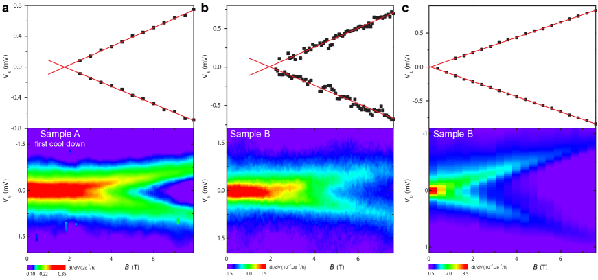
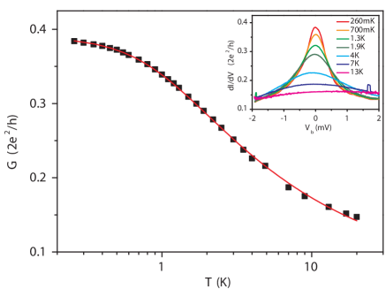
We now turn to the measurement of sample presented in Fig. 1d for the first cool down, for which a full experimental study in the case of even number of electrons is presented in reference Roch2008 . The charging energy can be extracted from the slope of the Coulomb diamond , using , where is the voltage spacing between successive charge states. For sample , we find meV. While the even-odd alternation is not totally clear, a sharp high-conductance ridge in the zero-bias differential conductance, is clearly observed in the vicinity of . Since the coherence of the system is suppressed and the Kondo effect disappears for a perturbation of energy larger than , we present in Fig. 2a a differential conductance measurement as a function of magnetic field up to T. A method to study the Kondo behavior and extract the typical energy scale , where denotes the Boltzmann’s constant, is to use the magnetic field dependence of the conductance Kogan2004 . The Zeeman effect competes with the Kondo resonance so that a non-equilibrium Kondo peak appears roughly at , where is the Landé factor, and denotes the Bohr magnetron, as shown in Fig. 2a. This spin-1/2 splitting is predicted to appear for Costi2000 , and the slope of the splitting is a direct measurement of the -factor of the quantum device. In Fig. 2a we linearly interpolate the position of these peaks and find = 1.78 T, which yields = 4.78 K, and . Another method to estimate the Kondo temperature is to measure the half width at half maximum (HWHM) of the peak for . At mK (inset of Fig. 3), we find , corresponding to K. A complementary method to estimate the Kondo temperature is to measure the evolution of the zero-bias conductance as a function of temperature, as presented in Fig. 3. The precise shape of this curve is universal (up to the value of energy scale ), and can be calculated by the Numerical Renormalization Group (NRG) theory Costi2000 . Following GoldhaberGordon1998 we fit the data using the empirical formula:
where is the conductance at , a fixed background conductance, and . We find = 4.46 K, which is in excellent agreement with the values determined previously, thus demonstrating a well defined Kondo energy scale.
Now, we turn to sample , for which a color-scale map of the differential conductance as a function of and is presented in Fig. 1b. By tuning from V to V, only one charge degeneracy point was observed. The charging energy of this SMT is then much higher ( meV) than for sample , and may indicate that we are not addressing the same redox state of the SMT, or that the coupling to the electrodes is lower than for sample . However, zero-bias anomalies are measured on both sides of the degeneracy point. We present the evolution of these zero-bias anomalies as a function of magnetic field on the right side (Fig. 2b) and the left side (Fig. 2c) of the degeneracy point. On the right side, from = T, we obtain = K, while from , we extract K. The value of obtained with the two different methods are comparable. Moreover, by linearly interpolating the position of this peaks, we find .
However, if we now focus on the left side of the degeneracy point, we measure = mT, and obtain = mK, while . However, from , we extract K, which is one order of magnitude higher than the value obtained with . If we assume a spin-1/2 Kondo effect on the right Coulomb diamond then the occupation number of the left diamond must be even. Therefore this large discrepancy in the two different methods of determining the Kondo temperature on the left Coulomb diamond, leads us to the hypothesis of a spin-1 Kondo effect. While a complete Kondo screening of the two-electron states is in principle possible Sasaki2000 , the one order of magnitude of difference in the determination of the Kondo temperature indicates that we may measure an underscreened spin-1 Kondo effect Roch2008 . Unfortunately, we did not perform a temperature dependent measurement of this differential conductance peak, thus we can not fully characterize this underscreened spin-1 Kondo effect.
We gratefully acknowledge E. Eyraud, D. Lepoittevin for useful electronic and dilution technical contributions and motivating discussions. We thank E. Bonet, T. Crozes and T. Fournier for lithography development. Samples were fabricated in the NANOFAB facility of the Institut Néel. This work is partially financed by ANR-PNANO.
References
- (1) H. Park et al.. Nature 407, 57 (2000).
- (2) J. Park et al.. Nature 417, 722 (2002).
- (3) D. R. Ward, G. D. Scott, Z. K. Keane, N. J. Halas & D. Natelson. cond. mat., http://arxiv.org/pdf/0802.3902 (2008).
- (4) W. Liang, M. P. Shores, M. Bockrath, J. R. Long & H. Park. Nature 417, 725 (2002).
- (5) S. Kubatkin et al.. Nature 425, 698 (2003).
- (6) A. R. Champagne, A. N. Pasupathy & D. C. Ralph. Nano Lett. 5, 305 (2005).
- (7) F. Elste & C. Timm. Phys. Rev. B 71, 155403 (2005), and references therein.
- (8) L.I. Glazman & M. E. Raikh. JETP letters 47, 452 (1988).
- (9) T. K. Ng & P. A. Lee. Phys. Rev. Lett. 61, 1768 (1988).
- (10) D. Goldhaber-Gordon et al.. Nature 391, 156 (1998).
- (11) S. M. Cronenwett, T. H. Oosterkamp & L. P. Kouwenhoven. Science 281, 540 (1998).
- (12) J. Nygård, D. H. Cobden & P. E. Lindelof. Nature 408, 342 (2000).
- (13) L. H. Yu & D. Natelson. Nano Lett. 4, 79 (2004).
- (14) A. N. Pasupathy et al. Science 306, 86 (2004).
- (15) J. J. Parks et al. Phys. Rev. Lett. 99, 026601 (2007).
- (16) H. Park, A. K. L. Lim, A. P. Alivisatos, J. Park & P. L. McEuen. Appl. Phys. Lett. 75, 301 (1999).
- (17) D. R. Strachan et al. Appl. Phys. Lett. 86, 043109 (2005).
- (18) G. Esen & M. S. Fuhrer. Appl. Phys. Lett. 87, 263101 (2005).
- (19) M. L. Trouwborst, S. J. van der Molen & B. J. van Wees. J. Appl. Phys. bf 99, 114316 (2006).
- (20) K. O’Neill, E. A. Osorio & H. S. J. van der Zant. Appl. Phys. Lett. 90, 133109 (2007).
- (21) Z. M. Wu et al. Appl. Phys. Lett. 91, 053118 (2007).
- (22) H. S. J. van der Zant et al. Faraday Discuss. 131, 347 (2006).
- (23) T. Taychatanapat, K. I. Bolotin, F. Kuemmeth & D. C. Ralph Nano Lett. 7, 652 (2006).
- (24) N. Roch, S. Florens, V. Bouchiat, W. Wernsdorfer & F. Balestro. Nature 453, 347 (2008).
- (25) M. F. Lambert, M. F. Goffman, J. P. Bourgoin & P. Hesto. Nanotechnology 14, 772 (2003).
- (26) A. A. Houck, J. Labaziewicz, E. K. Chan, J. A. Folk & I. L. Chuang. Nano Lett. 5, 1685 (2005).
- (27) A. S. Kogan et al. Phys. Rev. Lett. 93, 166602 (2004).
- (28) S. Sasaki et al. Nature 405, 764 (2000).
- (29) T. A. Costi. Phys. Rev. Lett. 85, 1504 (2000).
- (30) D. Goldhaber-Gordon et al. Phys. Rev. Lett. 81, 5225 (1998).