Spin-orbit interaction and spin relaxation in a two-dimensional electron gas
Abstract
Using time-resolved Faraday rotation, the drift-induced spin-orbit field of a two-dimensional electron gas in an InGaAs quantum well is measured. Including measurements of the electron mobility, the Dresselhaus and Rashba coefficients are determined as a function of temperature between 10 and 80 K. By comparing the relative size of these terms with a measured in-plane anisotropy of the spin-dephasing rate, the D’yakonv-Perel’ contribution to spin dephasing is estimated. The measured dephasing rate is significantly larger than this, which can only partially be explained by an inhomogeneous factor.
The possibility to manipulate spins in semiconductors is a requirement for future spin-based information processing. Awschalom2007 Using the spin-orbit (SO) interaction Dresselhaus1955 ; Bychkov1984 is a promising way to precisely control spin polarization because of its simple principle based on external gate electrodes. Datta1990 ; Hall2006 Manipulation of spins using the SO interaction has been shown in various semiconductor systems, such as bulk semiconductors Kato2004 , two-dimensional electron gases Meier2007 (2DEGs), and even quantum dots containing only one single electron. Nowack2007 On the other hand, the SO interaction is a source for spin dephasing. In 2DEGs, the SO interaction induces a linear -dependent splitting. Silsbee2004 This splitting gives rise to an effective magnetic field, leading to dephasing of the polarized electron spins. Dyakonov1972 This effect is known as the D’yakonv-Perel’ (DP) mechanism, and its control through manipulation of the SO interaction has been proposed Schliemann2003 as an alternative to the ballistic spin transistor. Datta1990 A careful engineering of the SO interaction is therefore crucial for using it to manipulate the spin.
In a 2DEG at intermediate temperatures, it is often assumed that the spin decay is governed by the DP mechanism. Zutic2004 ; Malinowski2000 Based on this assumption, information on the SO interaction in semiconductor quantum wells (QWs) was obtained from measurements of the spin-dephasing rate. Averkiev2006 ; Eldridge2007 ; Larionov2008 An independent measurement of the relative size of the SO interaction in (110)-grown QWs using the photogalvanic effect has been described in Ref. Belkov2008, and compared to the spin decay time. In this paper, we report on quantitative and independent measurements of the SO interaction and the spin-dephasing rate in an InGaAs QW, utilizing time-resolved Faraday rotation. In a further development of the method described in Ref. Meier2007, , a well-defined current is applied in the 2DEG using Ohmic contacts and a mesa structure (in Ref. Meier2007, , the electron drift was induced by an ac voltage applied to Schottky contacts in an unstructured 2DEG). The drifting electrons see an effective SO magnetic field, in the following referred to as drift SO field. The sizes of its two contributions, the Rashba Bychkov1984 and the Dresselhaus Dresselhaus1955 fields, are determined as a function of temperature from the measured influence of the in-plane electron drift velocity on the spin precession. Comparing our results with measured spin-dephasing rates and their in-plane anisotropy, we find that DP is not the only mechanism for spin decay in our samples at between 10 and 80 K.
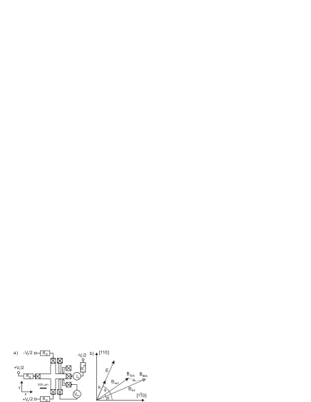
The 2DEG we use in this work is located in an In0.1Ga0.9As/GaAs QW. Electrons are confined to a 20-nm-thick In0.1Ga0.9As layer that is -doped (3 cm-3) to ensure a small electron scattering time such that we are in the dirty limit of the SO interactionSilsbee2004 , where the frequency of spin precession about the SO fields is small compared with the momentum scattering rate ( for our samples). On both sides of this layer, there is a 10-nm-thick GaAs spacer layer and a 10-nm-thick layer of -doped GaAs. A 10 nm cap of undoped GaAs completes the structure, grown by molecular beam epitaxy and forming a 2DEG 40 nm below the surface. We use wet etching to pattern a cross-shaped mesa as shown in Fig. 1(a) and create standard AuGe Ohmic contacts in the four ends of the cross. Four additional contacts on one arm of the cross allow its use as a Hall bar to determine the resistivity and carrier density of the 2DEG. Two samples with the same structure are glued into one chip carrier, whereby one sample is rotated by 90∘ to allow the SO interaction to be measured in one cool-down. At 40 K, the two-point resistance of the crosses in or direction is 4.1 k. We use additional resistors k to compensate for small variations in the contact resistance and apply voltages and as shown in Fig. 1(a). All angles are given with respect to the axis along , as seen in Fig. 1(b). We obtain the resistivity of the 2DEG during optical experiments monitoring the ratio of the voltage drop and the current through one arm of the mesa [see Fig. 1(a)], and measure a value of 770 /sq at 40 K. The voltages and create an electric field in the center of the cross in direction and with an amplitude proportional to . Because is monitored, the corresponding component of can be determined directly (see below). The electric field shifts the Fermi circle by an amount of , where is the effective electron mass, is the electron mobility, and is Planck’s constant divided by . In the dirty SO limit, the shift induces drift SO fields that can be expressed as Silsbee2004
| (1) |
with , is the electron factor, is the Bohr magneton, and and are the Rashba and Dresselhaus spin-orbit coefficients, respectively. The Rashba field has its origin in the structure inversion asymmetry (SIA) due to nonuniform doping on both sides of the QW and the presence of the surface on one side of the QW. The Dresselhaus field is a consequence of the bulk inversion asymmetry (BIA) of the zinc-blende structure. Cubic Dresselhaus terms do not change the linearity of in , but introduce a correction of , where is the Fermi wave number and the expectation value of the squared wave number along the growth direction . Taking a sheet density of m-2 (see below) and approximating by , where nm is the QW width, we obtain . This gives a correction in of about than 35%, which will be neglected in the following.
An external magnetic field is applied in the direction as seen in Fig. 1(b). The angles are for sample 1 and for sample 2. A transverse electron polarization precesses coherently about the vector sumKalevich1990 ; Engel2007 ; Duckheim2007 of and the drift SO fields defined in Eq. (1) with a frequency given by the modulus of this total field vector. If , the total field can be approximated as Meier2007
| (2) |
Because of the different angular dependencies of the Rashba and Dresselhaus SO fields, the two contributions can be distinguished. We use time-resolved Faraday rotation to determine the Larmor frequency of the spins precessing about . For this, the output of a pulsed Ti:sapphire laser with a repetition rate of 80 MHz is split into a pump and a probe beam. The pump/probe intensity ratio is 10/1 and, unless stated otherwise, the pump power is 500 W, focused onto a spot 30 m in diameter. The circularly polarized pump pulse is tuned to the absorption edge of the QW at 1.44 eV and creates a spin polarization along the growth axis of the QW. With a pump power of 500 W and assuming an absorption of about 1%Miller1982 we obtain a photo-excited carrier concentration on the order of a few cm-2, which is more than a magnitude smaller than the equilibrium carrier sheet density in the QW (see below). The Faraday rotation of the linear polarization axis of the probe pulse transmitted is proportional to the spin polarization along the QW growth axis. Changing the delay between pump and probe reveals the spin dynamics of the system, and the Faraday rotation angle can be described by . Here, is the amplitude of the Faraday signal and the spin dephasing time. A measurement of in a known magnetic field reveals an electron factor of , assuming that the factor is negative.
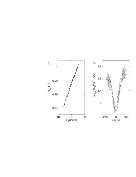
Figure 2(a) shows measured in the center of the cross as a function of the electric field between the two contacts in the right arm. These contacts are separated by a distance of = 100 m. is set to ground. The temperature of the sample is 40 K, and is oriented along the [110] direction, therefore . The data in Fig. 2(a) contain values from sweeps of up and down. The up and down sweeps fit nicely to a straight line, showing that we can exclude a drift of over time, which might be caused by nuclear polarization or drift of laser power or temperature.
As a result of the sample geometry and the grounded contacts to the left and the right of the center, the electric field in the center of the cross is reduced as compared to the value measured in the arm. By scanning the laser beam along the -axis and centered in the -direction [see Fig. 1(a)], we obtain a cross section of the drift SO field that is related to the electric field distribution.Meier2008 The resulting slopes of the linear fits of vs. are shown as a function of in Fig. 2(b). We see a pronounced dip in the center of the cross, which is explained by the reduced electric field. The solid line in Fig. 2(b) represents the solution of a numeric simulation of the electrostatics using a two-dimensional partial differential equation solver. Assuming that and are independent of the position and using the measured mobility (see below), the only fit parameter left is the difference . The measurement and the simulation are consistent and show that the electric field in the middle of the cross is 0.71 times smaller than the measured value . This correction is taken into account in the following when indicating electric-field values.
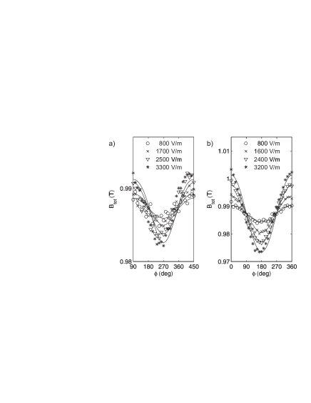
To disentangle and , we position the laser spot in the center of the cross and rotate the electric field. We did such experiments for different amplitudes of the electric field up to 3.3 kV/m and for two different configurations of . In Fig. 3(a), = , and in Fig. 3(b), = . The data are obtained at 20 K. oscillates in with an amplitude that is proportional to for and to for . The difference in the amplitude for the two cases (note the different scales) shows that and are comparable in relative strength and that the interplay of the two SO effects gives rise to an anisotropic spin splitting in space. The solid lines are a fit to the data using Eq. (2). Small deviations of the data from theory in the direction could result from a slight accidental off-center position of the laser spot.
To calculate the SO coefficients and from the measured and , we need a value for the drift momentum of the electrons. This is obtained from a Hall measurement of the sheet resistivity and the sheet carrier density . We calculate the mobility using , being the electron charge. In the dark, the resistivity of the 2DEG is approximately 1000 /sq and decreases to 770 /sq under conditions of the optical measurements. The Hall sheet densities are m-2 under illumination and m-2 in the dark. These densities are constant from 10 to 80 K. From Shubnikov–de Haas oscillations at K, we get a sheet density of m-2 under optical illumination. A small parallel conductivity of a doping layer could explain the difference in the two numbers. Such a parallel conductivity does not influence the optical experiments as these electrons do not contribute to the Faraday signal.
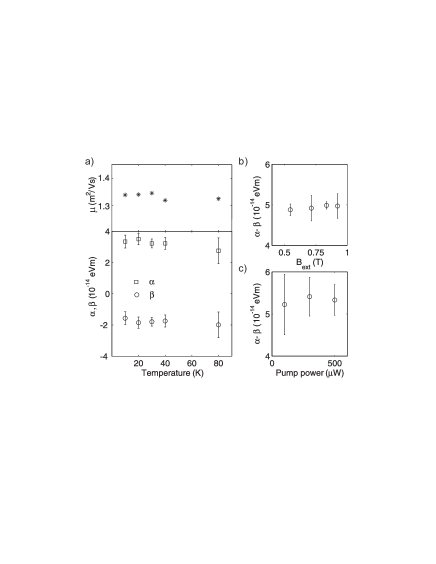
The mobilities extracted from the Hall measurement under illumination are shown in the upper inset of Fig. 4(a). The mobility does not change significantly over the temperature range measured. Using the results of the transport measurements and assuming that , we can calculate and use Eq. (1) to obtain and for all the temperatures measured. The results are displayed in Fig. 4(a). Error bars show a confidence interval. The wafer used for this work is the same as the one used for sample 3 in Ref. Meier2007, . We measure values for and that are by a factor of 2-3 smaller, which we attribute to a more precise determination of the electric field in this work. In addition, different wafer processing and oxidation of the wafer surface over time might influence the SO coefficients measured in this shallow 2DEG. Variations in and for subsequent cool downs are within the error bar. Note that we extrapolate the mobility and the electric field in the center of the cross from a transport measurement away from the center. We cannot exclude that we underestimate the absolute values for and because of a reduced electron drift momentum that might result from, e.g., screening by the optically excited charge carriers. The model of Viña Vina1984 with the results and the parameters used by Hübner et al. Huebner2006 predicts the dependence of the band parameters, from which we estimate the dependence of and using theory.Winkler2003 The calculated -induced change in and between 10 and 80 K is in the sub-percentage range and thus much smaller than our measurement error. Interestingly, in Ref. [Eldridge2007, ] a linear increase in with for higher was observed on a [110] QW, which the authors could not explain with theory.
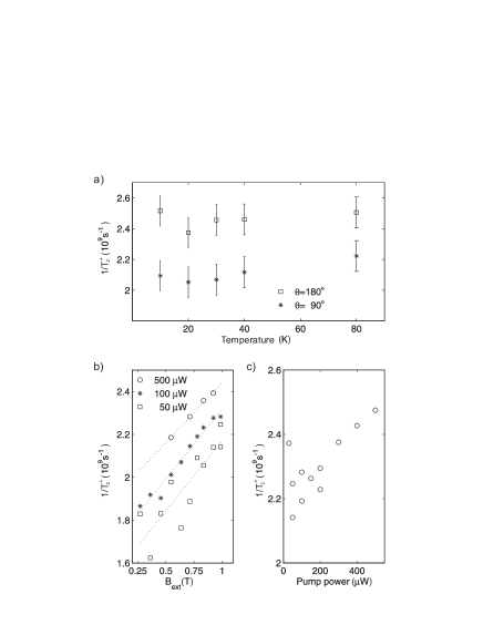
We find no dependence of the SO coefficients on , in
agreement with our assumption that the precession frequency is given
by the modulus of the vector sum of and the drift
SO fields given in Eq. (1). Figure 4(b)
shows a measurement of vs . The
insensitivity of the result on excludes a
significant admixture of a dependent and anisotropic factor,
as was stipulated in Ref. Margulis1983, . To test the
reliability of our method, we also checked whether a lower pump
power will influence the outcome of the measurement. This could
occur from, e.g., a population of higher energy states with larger
pump power. We found, however, that does not depend
significantly
on the pump power, as seen in Fig. 4(c).
When and are of similar magnitude, the spin lifetime is strongly anisotropic with respect to the direction of in the plane of the 2DEG. Averkiev1999 ; Averkiev2006 ; Schliemann2003 ; Duckheim2007 ; StichC2007 ; Larionov2008 This anisotropy is a consequence of the DP mechanism because the spins precess about a SO field whose direction becomes independent of for . From the measured anisotropy in and the relative size of and , we estimate the contribution from the DP mechanism to the spin dephasing. In Fig. 5(a), the spin relaxation rate 1/ is plotted as a function of for the two orientations of =0.99 T. The dependence is rather small, and we can clearly see an anisotropy of 1/, confirming the anisotropic spin splitting in our system. Because our 2DEG is well in the dirty SO limit, we can use the motional narrowing limit of the DP mechanism,Silsbee2004 where the spin dephasing due to -dependent SO fields is decreased by spin-preserving scattering. This gives the following expressions for the anisotropic spin decay rates:
| (3) |
Here, are the relaxation times of spins oriented along , , or . is a constant that depends on , Fermi energy, scattering time, and the scattering mechanism.Kainz2004 If we apply a large external magnetic field ( ), we can write the DP spin-dephasing rate as Larionov2008
| (4) |
For the difference, we get and read a value of about s-1 in Fig. 5(a) for the difference. Using the measured values for and , we get m-2eV-2s-1. From Eqs. (3) and (4), this yields relaxation rates for DP of about s-1 for , and of s-1 for . In Eq. (3), it is assumed that the SO splitting is linear in . As mentioned earlier, we are in a regime where . Taking into account the cubic Dresselhaus terms Kainz2004 we find only a small correction to the values for the spin relaxation rate obtained above. As the total 1/ lies between 2.1 and 2.5 s-1, other spin-dephasing mechanism must be present in our sample.
To exclude optical recombination as a source of decay of the Faraday signal, we measured the time-resolved reflection,Malinowski2000 which exponentially decays with a decay time of less than 100 ps (data not shown). Interpreting this time as the electron-hole recombination time provides evidence that the spin polarization, which is observable over a much longer time scale in the Faraday signal, must get imprinted onto the equilibrium electrons in the QW conductance band through recombination of unpolarized electrons and holes.Kikkawa1998 It is therefore justified to interpret the decay time of the Faraday signal fitted in a window from 80 to 1000 ps as the decay time .
From the dependence of on , information on the mechanism of spin dephasing can be obtained. The DP spin dephasing rate does not depend on in the motional narrowing regime and for .Ivchenko1973 In contrast to this, a -dependence that is intrinsic to the DP mechanism is observed in high-mobility samples.StichC2007 In our low-mobility samples, we find a linear increase in with , as shown in Fig. 5(b). Such a linear -dependence is evidence of an inhomogeneous dephasing due to a variation of the factor in the area of the 2DEG probed, described by a dephasing rate ,Kikkawa1998 ; Chen2007
| (5) |
We suspect that the factor variation could be a consequence of the in-well doping. That the sample is rather inhomogeneous is also seen in a photoluminescence experiment, in which we observe a broad luminescence peak from the QW (not shown) with a full width at half maximum of about 20 meV. We used different pump intensities and find a similar slope for the dashed linear fits in Fig. 5(b). The W measurement was done at 40 K, and the other two at 10 K. From these data, we conclude that is quite constant for different pump powers. From the slopes in Fig. 5(a) and using Eq. (5), we obtain . Unexpectedly in a doped sample with fast electron-hole recombination, the overall spin-relaxation rate increases with increasing pump power; see Fig. 5(c). In a high-mobility sample, a decrease in the spin relaxation-rate with increasing initial spin polarization has been observed, which goes into the opposite direction.StichB2007 In an attempt to minimize this pump-power dependence, we used a low pump power of 50 W for the measurement in Fig. 5(a).
| Relaxation mechanism | DP | Sum | Measured | |
|---|---|---|---|---|
| (1/s) | 0.6 | 0.7 | 1.30.2 | 2.1 0.1 |
| (1/s) | 1.0 | 0.7 | 1.70.2 | 2.5 0.1 |
Table 1 summarizes the contributions to the anisotropic 1/ for K. The calculated sum of the relaxation rate is by about s-1 lower than the measured value. This discrepancy indicates the presence of another spin-dephasing mechanism. A possible candidate is a random SO field originating from the Coulomb potential of ionized dopants or from surface roughness of the QW. It has been pointed out that such spatial fluctuations might limit the spin lifetime for symmetric (110) QWs (Ref. Karimov2003, ) or in the case where .Sherman2005 The importance of this effect is probably smaller in our samples where both and are finite but not equal in size. In a small-gap semiconductor, the Elliott-Yafet (EY) mechanism contributes to the spin dephasing.Elliott1954 By estimating the importance of the EY mechanismZutic2004 in our sample using the measured mobility and the known band parameters, we obtain a spin-relaxation rate on the order of 5 s-1. This is negligibly small, but there are indicationsTackeuchi1999 that the EY spin-dephasing rate might be larger than estimated with the equation derived for a bulk semiconductor.
The weak variation in with shown in Fig. 5(a) can be understood as a consequence of little temperature dependence of the individual contributions to . As pointed out in Ref. Kainz2004, , the DP dephasing rate depends only weakly on in the degenerate regime and in the intermediate temperature range, apart from its proportionality to the electron scattering time. As our mobility is quite constant over the temperature range measured, we do not expect large variations. We observe no evidence of a dependence of the factor spread on . For a degenerate electron density and a constant mobility, also the dependence of the EY mechanism should be small. The observed weak dependence is therefore not surprising, and has also been observed in other experiments. Malinowski2000
To conclude, we have measured the SO interaction coefficients and as a function of and find no significant dependence. From and , the measured Hall mobility and the anisotropy in , we estimate the contribution from DP spin dephasing, and find that DP alone cannot explain the measured . From a linear increase in with , we identify an inhomogeneous broadening from a spread in the electron factor. These effects do not account for all of the measured spin-dephasing rate. We speculate that EY or an inhomogeneous SO field might induce an additional isotropic contribution. A more detailed study of the nature of the elastic and inelastic electron-scattering mechanisms involved might facilitate an exact attribution to the different decay mechanisms.
We gratefully acknowledge helpful discussions with T. Ihn and I. Shorubalko and thank B. Küng for evaporating contact metals. This work was supported by the CTI and the SNSF.
References
- (1) D. D. Awschalom and M. E. Flatté, Nat. Phys. 3, 153 (2007).
- (2) G. Dresselhaus, Phys. Rev. 100, 580 (1955).
- (3) Y. A. Bychkov and E. I. Rashba, J. Phys. C 17, 6039 (1984).
- (4) S. Datta and B. Das, Appl. Phys. Lett. 56, 665 (1990).
- (5) K. C. Hall and M. E. Flatté, Appl. Phys. Lett. 88, 162503 (2006).
- (6) Y. Kato, R. C. Myers, A. C. Gossard, and D. D. Awschalom, Nature 427, 50 (2004).
- (7) L. Meier, G. Salis, I. Shorubalko, E. Gini, S. Schön, and K. Ensslin, Nature Phys. 3, 650 (2007).
- (8) K. C. Nowack, F. H. L. Koppens, Y. V. Nazarov, and L. M. K. Vandersypen, Science 318, 1430 (2007).
- (9) R. H. Silsbee, J. Phys. Condens. Matter 16, R179 (2004).
- (10) M. I. D’yakonov and V. I. Perel’, Sov. Phys. Solid State 13, 3023 (1972).
- (11) J. Schliemann, J. C. Egues, and D. Loss, Phys. Rev. Lett. 90, 146801 (2003).
- (12) I. Žutić, J. Fabian, and S. Das Sarma, Rev. Mod. Phys. 76, 323 (2004).
- (13) A. Malinowski, R. S. Britton, T. Grevatt, R. T. Harley, D. A. Ritchie, and M. Y. Simmons, Phys. Rev. B 62, 13034 (2000).
- (14) N. S. Averkiev, L. E. Golub, A. S. Gurevich, V. P. Evtikhiev, V. P. Kochereshko, A. V. Platonov, A. S. Shkolnik, and Y. P. Efimov, Phys. Rev. B 74, 033305 (2006).
- (15) P. S. Eldridge, W. J. H. Leyland, P. G. Lagoudakis, O. Z. Karimov, M. Henini, D. Taylor, R. T. Phillips, and R. T. Harley, Phys. Rev. B 77, 125344 (2008).
- (16) A. V. Larionov and L. E. Golub, Phys. Rev. B 78, 033302 (2008).
- (17) V. V. Bel’kov, P. Olbrich, S. A. Tarasenko, D. Schuh, W. Wegscheider, T. Korn, C. Schüller, D. Weiss, W. Prettl, and S. D. Ganichev, Phys. Rev. Lett. 100, 176806 (2008).
- (18) V. K. Kalevich and V. L. Korenev, JETP Lett. 52, 230 (1990).
- (19) H.-A. Engel, E. I. Rashba, and B. I. Halperin, Phys. Rev. Lett. 98, 036602 (2007).
- (20) M. Duckheim and D. Loss, Phys. Rev. B 75, 201305 (2007).
- (21) D. A. B. Miller, D. S. Chemla, D. J. Eilenberger, P. W. Smith, A. C. Gossard, and W. T. Tsang, Appl. Phys. Lett. 41, 679 (1982).
- (22) L. Meier, G. Salis, E. Gini, I. Shorubalko, and K. Ensslin, Phys. Rev. B 77, 035305 (2008).
- (23) L. Viña, S. Logothetidis, and M. Cardona, Phys. Rev. B 30, 1979 (1984).
- (24) J. Hübner, S. Dohrmann, D. Hägele, and M. Oestreich, arXiv:cond-mat/0608534 (2006).
- (25) R. Winkler, Spin-Orbit Coupling Effects in Two-Dimensional Electron and Hole Systems (Springer, Berlin, 2003).
- (26) A. D. Margulis and V. A. Margulis, Sov. Phys. Solid State 25, 918 (1983).
- (27) N. S. Averkiev and L. E. Golub, Phys. Rev. B 60, 15582 (1999).
- (28) D. Stich, J. H. Jiang, T. Korn, R. Schulz, D. Schuh, W. Wegscheider, M. W. Wu, and C. Schüller, Phys. Rev. B 76, 073309 (2007).
- (29) J. Kainz, U. Rössler, and R. Winkler, Phys. Rev. B 70, 195322 (2004).
- (30) J. M. Kikkawa and D. D. Awschalom, Phys. Rev. Lett. 80, 4313 (1998).
- (31) E. L. Ivchenko, Sov. Phys. Solid State 15, 1048 (1973).
- (32) Z. Chen, S. G. Carter, R. Bratschitsch, P. Dawson, and S. T. Cundiff, Nature Phys. 3, 265 (2007).
- (33) D. Stich, J. Zhou, T. Korn, R. Schulz, D. Schuh, W. Wegscheider, M. W. Wu, and C. Schüller, Phys. Rev. B 76, 205301 (2007).
- (34) O. Z. Karimov, G. H. John, R. T. Harley, W. H. Lau, M. E. Flatté, M. Henini, and R. Airey, Phys. Rev. Lett. 91, 246601 (2003).
- (35) E. Y. Sherman and J. Sinova, Phys. Rev. B 72, 075318 (2005).
- (36) R. J. Elliott, Phys. Rev. 96, 266 (1954).
- (37) A. Tackeuchi, T. Kuroda, S. Muto, Y. Nishikawa, and O. Wada, Jpn. J. Appl. Phys 38, 4680 (1999).