Reversable heat flow through the carbon nanotube junctions
Abstract
Microscopic mechanisms of externally controlled reversable heat flow through the carbon nanotube junctions (NJ) are studied theoretically. Our model suggests that the heat is transfered along the tube section by electrons () and holes () moving ballistically in either in parallel or in opposite directions and accelerated by the bias source-drain voltage (Peltier effect). We compute the Seebeck coefficient , electric and thermal conductivities and find that their magnitudes strongly depend on and . The sign reversal of versus the sign of formerly observed experimentally is interpreted in this work in terms of so-called chiral tunneling phenomena (Klein paradox).
pacs:
73.23.Hk, 73.63.Kv, 73.40.GkPhysics of the heat transfer determines functionality, precision and effectiveness of solid state nanocoolersNC1 ; NC2 ; NC3 ; Kim which are environment friendly and have a lot of applications in the experimental physics, nanoelectronics, chemistry, industry and medicine. Therefore exploiting of new thermoelectric materials with high figures of merit ( being the temperature) attracts a lot of attention. Recently such interest arose toward the carbon nanotube and graphene junctions which electronic properties are highly unconventional Kim . The thermoelectric power experiments Kim addressed single wall carbon nanotube junctions. In Ref. Kim a temperature difference induced a finite bias voltage across the junction which sign changed versus the gate voltage . A question here is how that unconventional thermoelectric behavior is related to the intrinsic nature of the carbon nanotube and graphene? It is widely accepted that the charge carrier motion in carbon nanotubes and in graphene is essentially phase-correllated. For such a reason the conducting electrons and holes in that materials behave as relativistic massless ’chiral fermions’ (CF) characterized by a ’pseudospin’ (see review Ando-rev and references thereis).
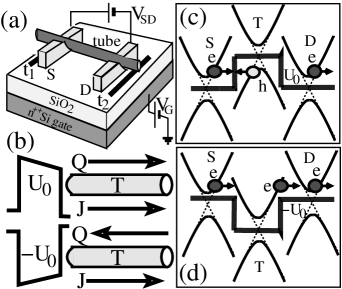
In this Letter we argue that the phase-correlated thermoelectric transport of charge carriers implicates a voltage-controlled and reversable heat flow through the single wall carbon nanotube junctions (Peltier effect). The enhancement of in those 1D devices where the charge carriers propagate ballistically occurs due to strong van Hove singularities (VHS). The VHS position is tuned by the gate voltage in respect to the Fermi level of the electrodes. When an VHS and match each other, it results in a sufficient density of charge carriers which contribute to the electric conductivity despite the Fermi energy itself is relatively small. A finite gate voltage is not just merely supplies either the electrons or holes into , but rather creates a potential barrier () or well () for chiral fermions transmitted across the junction as illustarted in Figs. 1(b-d). A finite sorce-drain d.c. bias voltage applied across the junction tilts the chiral barrier and causes the electric charge carriers to accelerate. This means that the energy of the charge carriers changes by , which inflicts a local temperature change at the corresponding junction′s end. The sign of (and hence of ) depends on whether the charge carriers inside the barrier are electrons or holes. Other thermal characteristics of the carbon nanotube and graphene junctions depend on precise microscopic mechanisms acting on the nanoscale. The setup shown in Fig. 1 allows controlling the sign of by merely flipping the sign of the gate voltage [see the sketch in Fig. 1(b)]. The source (S) and drain (D) electrodes can either be metallic or made of the nanotube/graphene itself. The potential chiral barrier is induced by the gate voltage from a Si gate. If , the transport mechanism is the chiral tunneling (CT). It presumes a constructive quantum interference between an incoming electron () and a hole () moving inside the graphene barrier in a reverse direction and is characterized by the same pseudospin as sketched in Fig. 1(c) (Klein paradoxStrange ; Krekora ). The interference pattern resulting from the chiral tunneling is very sensitive to the phase difference between the and wavefunctions. During the CT process the electric current is transferred by holes, which ballistically propagate in a reverse direction. That means the heat and the electric current are directed in antiparallel. When the gate voltage is reversed (), the heat and the electric current flow in parallel, since both of them are transferred by electrons. This reverses the heat flow along as compared to the former case . We emphasize that the reversable heat flow originates from the phase correlation between the electrons and holes which constitutes its quantum mechanical origin. Our finding suggest that the thermoelectric transport serves as another independent probe of the phase-coherence in the carbon nanotube junctions.
Thermoelectric transport properties of the Peltier coolers are characterized by the figure of merit . For a symmetric setup shown in Fig. 2(c) takes the form
| (1) |
In Eq. (1) the lattice thermal conductivity is , is the graphene heat capacity, which at is J/(molK), is the graphene sound velocity, where m/s is the Fermi velocity in graphene, is the phonon free path inside the nanotube. A most conservative estimation used here implies that is comparable with the tube diameter, i.e., . The Seebeck coefficient of electron (+) and holes (-), , is obtained as , where is the electric charge of the electron (hole). Besides in Eq. (1) is the conductivity of two equal size conducting tubes connected in a sequence, where and is the electron (hole) thermal conductivity . The functions entering the above formulas are
| (2) |
The functions are computed from a microscopic model. If one neglects by detailed energy dependence of and merely sets , then where is the electron density of states at the Fermi level of electrodes, and
| (3) |
and the electron (hole) thermal conductivity becomes
| (4) |
The estimations using Eqs. (1)-(4) give the figure of merit for a symmetric setup as
| (5) |
where , . One may notice that does not depend on the properties of electrodes but instead strongly depends on and . For the product may be increased by 2 orders of magnitude when neglecting by the phonon heat conductivity. In Eq. (3)-(5) we used that , and . The above rough estimations illustrate the temperature behaviour of the figure of merit disregarding however the microscopic mechanisms of the thermoelectric transport. A deeper understanding is achieved with using of a microscopic model where the electron and hole envelope wave functions satisfy the Dirac equation. That model allows computing the transparency of the chiral barrier and well shown in Fig. 1(b-d). We calculate the steady state thermoelectric characteristics of an NJ with metallic electrodes controlled by the gate voltage and biased by the source-drain voltage . In particular we will see that the gate voltage reverses the heat flow along , which is well consistent with the earlier experimentsKim . The figure of merit strongly increases at certain magnitudes of and . The source drain bias voltage in our setup drops entirely on the nanotube [see its profile below Fig. 1(b)], which corresponds to a trapezoidal shape of the chiral barrier tilted proportionally to . For the NJ having finite dimensions, the motion of CF is quantized. The quantization imposes additional constrains on the directional tunneling diagram. The Dirac equation for fermions is written as
| (6) |
where is the massless fermion speed, is the CF energy, and are the Pauli matrices, , the barrier potential is induced by the gate voltage . In the steady state, when the EF is off, the electric current is fully suppressed when (for typical gate voltage V and the SiO2 thickness nm one findsJapan2 meV). The CF energy in the leads ( and ) reads where is the Fermi wavevector in the S and D electrodes. Then in the electrodes one takes . Inside the tube one uses , where the electron wave vector in the transverasal direction is , is the nanotube diameter, is the electron subband index, , , , and are integer numbers related to the translation vector of the graphene lattice, and are primitive translation vectors. In particular index when the tube is metallic while for semiconducting and dielectric tubes.
In a simplest case from continuous boundary conditions one gets
| (7) |
where , is the tube length, , , , , . The transmission amplitude is computed using a simple approach, which represents the CF envelope wavefunctions as plane waves for a rectangular barrier and via Airy functionsKorn for a trapezoidal barrier. In particular, the scattering state for a trapezoidal barrier is constructed as
| (8) |
where and are the Airy functions, and we also introduced the auxiliary functions where means the Kronecker product, and are 12 matrices, , where signs apply to conductive (valence) bands, is positive for conductance band and negative for the valence band, the factor satisfies the identity . Then one implements the above Eqs. (1)-(2), and (7) to obtain , , , and .
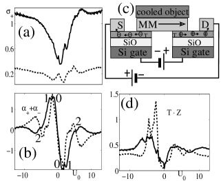
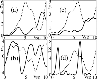
Our theoretical model interpretes the experimental data of Ref. Kim in terms of chiral tunneling. We find that the electric and heat transport characteristics of the nanotube junctions are pretty much determined by details of their electron spectrum. In particular, the electric and heat transport characteristics of the semiconducting nanotube (with ) junctions shown in Fig. 2 for two SWCNT diameters (dashed curves) and (solid curves) computed at remarkably depend on the barrier height . The d.c. electric conductivity plotted in units of in Fig. 2(a) shows a huge dip in vicinity of , which comes from the dispersion law in the lowest subband with . The upper electron subbands with give a fine structure in the transport characteristics which is remakably pronounced in all the , , , and curves, as is evident from Fig. 2. To distinguish the contributions from different electron subbands with we mark the corresponding features by indices 0,1,2 in Fig. 2(b). The positions and magnitudes of those features reflect the electron band structure of the tube or the graphene stripe. Similar fine structure features coming from different electron subbands are visible also in Figs. 2(a), (c,d) for two the SWCNT diameters (dashed curve) and (solid curve) computed at and . The reversable heat flow due to the chiral tunneling is well pronounced in the Seebeck coefficient . In Fig. 2(b) we plot the net Seebeck coefficient [in units of ]. One see that reverses its sign as the sign of changes. This sign change along with the specific one-dimensional bandstructure of the single wall carbon nanotubes can be exploited for creating of very efficient Peltier nanocoolers. An example of that cooler setup is sketched in Fig. 2(c). The reversable Peltier nanocooler is combined of two NJs [see the former Fig. 1(a)] with individual gate voltage control for each of the tube. A significant enhancement of the figure of merit in those 1D devices is achieved by matching of the van Hove singularities (VHS) with position of the Fermi level in the electrodes by changing the gate voltage and the bias voltage . The aforementioned peculiarities coming from the chiral tunneling and from the electron band structure actually determine behavior of versus shown in Fig. 2(d). From that Fig. 2(d) one can see that for the semiconducting () tube with diameter the product may exceed 1. Further improvement of the product about by one order of magnitude is acomplished by applying a finite bias voltage as shown in plots of , , , and in Fig. 3(a-d). The transport coefficients were computed at the temperature (in units , which for mV corresponds K). One may notice that the product also depends on the tube diameter . For a thinner tube with one gets already at while for the thicker tube one achieves by applying a much higher bias voltage . Similar double peak structure coming from matching of the VHSs with of electrodes [see solid curve in Fig. 3(d)] had also been proclaimed in Bi nanowires Dress . More significant increase of the product is obtained at lower temperatutes. Using the cooler setup shown in Fig. 2(c) one may potentially get even for temperatures K down to 1 K and with an appropriate tuning by and simultaneously. Inclusion of the Shottky barriers and Coulomb blockade in the present model is pretty straiforward and will be given elsewhere. Our study indicates that narrow semiconducting single wall CNTs are more efficient in coolers than metallic CNT and graphene stripes (where there is no VHS for the lower subband ). An evident reason is that the matching of VHSs with in electrodes results in a better cooling performance. Another strong benefit of the NJ cooler is that one avoids a mutual compensation of and in Eq. 1 as it happens, e.g., for Bi nanowire cooler (see Ref. Dress ) since one appropriately flips signs of merely by changing .
In conclusion we suggested a theoretical model of the electric and heat transport across the carbon nanotube junction. We find that the heat transport strongly depends on the polarity and magnitude of the source-drain and gate voltages. That voltages tune the basic transport properties of the carbon nanotubes via affecting of their electronic structure and phase-correlated transport of charge carriers. Due to resonant character of chiral tunneling and low inelastic scattering rates the heat current density is typically much higher than in ordinary semiconducting devices. At the same time, the Peltier effect is well pronounced up to relatively high temperatures. The reversable Peltier effect shows great promises for cooling nanodevices and termometers.
I wish to thank H. Weinstock, V. Chandrasekhar, P. Barbara, A. Sergeev and H. Espinosa for fruitful discussions.
References
- (1) Thermoelectric Handbook, edited by D. M. Rowe (Chemical Rubber Company, Boca Raton, Florida, 1995), pp. 407 and 390.
- (2) L. D. Hicks and M. S. Dresselhaus, Phys. Rev. B 47, 12 727 (1993); 47, 16 631 (1993); Y.-M. Lin, X. Sun, and M. S. Dresselhaus, Phys. Rev. B 62, 4610 (2000).
- (3) M. F. Lin, D. S. Chuu, K. W. K. Shung, Phys. Rev. B 53, 11186 (1996).
- (4) X. Sun, Z. Zhang, and M. S. Dresselhaus, Appl. Phys. Lett., 74, 4005 (1999).
- (5) J. P. Small, K. M. Perez, and P. Kim, Phys. Rev. Lett. 91, 256801 (2003).
- (6) T. Ando, J. Phys. Soc. Jpn. 74, 777 (2005).
- (7) S. E. Shafranjuk, Phys. Rev. B76, 085317 (2007).
- (8) P. Strange, Relativistic Quantum Mechanics (Cambridge University Press, Cambridge, UK, 1998).
- (9) P. Krekora, Q. Su and R. Grobe, Phys. Rev. Lett. 92, 040406 (2004).
- (10) Japanese, Science 306, 666 (2004);
- (11) A. L. Yeyati and M. Büttiker, Phys. Rev. B 52, R14360 (1995).
- (12) L. V. Keldysh, Sov. Phys. JETP 20, 1018 (1965).
- (13) S. Datta, Electronic Transport in Mesoscopic Systems (Cambridge University Press, Cambridge, UK, 1997).
- (14) M. I. Katsnelson, K. S. Novoselov, and A. K. Geim, Nature Phys. 2, 620 (2006).
- (15) G. A. Korn and T. M. Korn, Handbook for Scientists and Engineers, McGraw-Hill (1967).