Abstract
A photonic crystal nanocavity with a Quality () factor of , a mode volume of 0.55()3, and an operating wavelength of 637 nm is designed in a silicon nitride (SiNx) ridge waveguide with refractive index of 2.0. The effect on the cavity factor and mode volume of single diamond nanocrystals of various sizes and locations embedded in the center and on top of the nanocavity is simulated, demonstrating that is achievable for realistic parameters. An analysis of the figures of merit for cavity quantum electrodynamics reveals that strong coupling between an embedded diamond nitrogen-vacancy center and the cavity mode is achievable for a range of cavity dimensions.
Design of an ultrahigh Quality factor silicon nitride photonic crystal nanocavity for coupling to diamond nanocrystals
Murray W. McCutcheon and Marko Lončar
School of Engineering and Applied Science, Harvard University, Cambridge, MA, 02138
murray@seas.harvard.edu
OCIS codes: (230.5298) Photonic crystals; (230.5750) Optical devices, resonators; (270.5580) Quantum electrodynamics
References and links
- [1] R. Miller, T. E. Northrup, K. M. Birnbaum, A. Boca, A. D. Boozer, and H. J. Kimble, “Trapped atoms in cavity QED: coupling quantized light and matter,” Journal of Physics B 38, S551–S565 (2005).
- [2] H. Walther, B. T. H. Varcoe, B.-G. Englert, and T. Becker, “Cavity quantum electrodynamics,” Reports on Progress in Physics 69, 1325–1382 (2006).
- [3] C. Weisbuch, M. Nishioka, A. Ishikawa, and Y. Arakawa, “Observation of the coupled exciton-photon mode splitting in a semiconductor quantum microcavity,” Phys. Rev. Lett. 69, 3314–3317 (1992).
- [4] T. Yoshie, A. Scherer, J. Hendrickson, G. Khitrova, H. M. Gibbs, G. Rupper, C. Ell, O. B. Shchekin, and D. G. Deppe, “Vacuum Rabi splitting with a single quantum dot in a photonic crystal nanocavity,” Nature 432, 200–203 (2004).
- [5] J. P. Reithmaier, G. Sek, A. Loffler, C. Hofmann, S. Kuhn, S. Reitzenstein, L. V. Keldysh, V. D. Kulakovskii, T. L. Reinecke, and A. Forchel, “Strong coupling in a single quantum dot-semiconductor microcavity system,” Nature 432, 197–200 (2004).
- [6] K. Hennessy, A. Badolato, M. Winger, D. Gerace, M. Atature, S. Gulde, S. Falt, E. L. Hu, and A. Imamoglu, “Quantum nature of a strongly coupled single quantum dot-cavity system,” Nature 445, 896–899 (2007).
- [7] K. Srinivasan and O. Painter, “Linear and nonlinear optical spectroscopy of a strongly coupled microdisk-quantum dot system,” Nature 450, 862–865 (2007).
- [8] D. Englund, A. Faraon, I. Fushman, N. Stoltz, P. Petroff, and J. Vučković, “Controlling cavity reflectivity with a single quantum dot,” Nature 450, 857–861 (2007).
- [9] L. Childress, M. V. G. Dutt, J. M. Taylor, A. S. Zibrov, F. Jelezko, J. Wrachtrup, P. R. Hemmer, and M. D. Lukin, “Coherent dynamics of coupled electron and nuclear spins in diamond,” Science 314, 281–285 (2006).
- [10] C. Kurtsiefer, S. Mayer, P. Zarda, and H. Weinfurter, “Stable solid-state source of single photons,” Phys. Rev. Lett. 85, 290–293 (2000).
- [11] T. Gaebel, M. Domhan, I. Popa, C. Wittmann, P. Neumann, F. Jelezko, J. R. Rabeau, N. Stavrias, A. D. Greentree, S. Prawer, J. Meijer, J. Twamley, P. R. Hemmer, and J. Wachtrup, “Room-temperature coherent coupling of single spins in diamond,” Nature Physics 2, 408–413 (2006).
- [12] M. V. G. Dutt, L. Childress, L. Jiang, E. Togan, J. Maze, F. Jelezko, A. S. Zibrov, P. R. Hemmer, and M. D. Lukin, “Quantum register based on individual electronic and nuclear spin qubits in diamond,” Science 316, 1312–1316 (2007).
- [13] C. Santori, P. Tamarat, P. Neumann, J. Wrachtrup, D. Fattal, R. G. Beausoleil, J. Rabeau, P. Olivero, A. D. Greentree, S. Prawer, F. Jelezko, and P. Hemmer, “Coherent population trapping of single spins in diamond under optical excitation,” Phys. Rev. Lett. 97, 247401 (2006).
- [14] R. Hanson, F. M. Mendoza, R. J. Epstein, and D. D. Awschalom, “Polarization and readout of coupled single spins in diamond,” Phys. Rev. Lett. 97, 087601 (2006).
- [15] J. Meijer, B. Burchard, M. Domhan, C. Wittmann, T. Gaebel, I. Popa, F. Jelezko, and J. Wrachtrup, “Generation of single color centers by focused nitrogen implantation,” Appl. Phys. Lett. 87, 261909 (2005).
- [16] F. Jelezko, T. Gaebel, I. Popa, M. Domhan, A. Gruber, and J. Wrachtrup, “Observation of coherent oscillations in a single electron spin,” Phys. Rev. Lett. 92, 076401 (2004).
- [17] A. D. Greentree, J. Salzman, S. Prawer, and L. C. L. Hollenberg, “Quantum gate for switching in monolithic photonic-band-gap cavities containing two-level atoms,” Phys. Rev. A 73, 013818 (2006).
- [18] J. I. Cirac, P. Zoller, H. J. Kimble, and H. Mabuchi, “Quantum state transfer and entanglement distribution among distant nodes in a quantum network,” Phys. Rev. Lett. 78, 3221–3224 (1997).
- [19] S. J. van Enk, J. I. Cirac, and P. Zoller, “Ideal quantum communication over noisy channels: A quantum optical implementation,” Phys. Rev. Lett. 78, 4293–4296 (1997).
- [20] Y.-S. Park, A. K. Cook, and H. Wang, “Cavity QED with diamond nanocrystals and silica microspheres,” Nano Letters 6, 2075–2079 (2006).
- [21] S. Tomljenovic-Hanic, M. J. Steel, and C. M. de Sterke, “Diamond based photonic crystal microcavities,” Opt. Express 14, 3556–3562 (2006).
- [22] C. Kreuzer, J. Riedrich-Moller, E. Neu, and C. Becher, “Design of photonic crystal microcavities in diamond films,” Opt. Express 16, 1632–1644 (2008).
- [23] I. Bayn and J. Salzman, “Utra high- photonic crystal nanocavity design: The effect of a low-index slab material,” Opt. Express 16, 4972 (2008).
- [24] C. F. Wang, R. Hanson, D. D. Awschalom, E. L. Hu, T. Feygelson, J. Yang, and J. E. Butler, “Fabrication and characterization of two-dimensional photonic crystal microcavities in nanocrystalline diamond,” Appl. Phys. Lett. 91, 201112 (2007).
- [25] K. Rivoire, A. Faraon, and J. Vučković, “Gallium phosphide photonic crystal nanocavities in the visible,” Appl. Phys. Lett. 93, 063103 (2008).
- [26] P. E. Barclay, K. Srinivasan, O. Painter, B. Lev, and H. Mabuchi, “Integration of fiber-coupled high- SiNx microdisks with atom chips,” Appl. Phys. Lett. 13, 801 (2005).
- [27] M. Eichenfeld, C. P. Michael, R. Perahia, and O. Painter, “Actuation of micro-optomechanical systems via cavity-enhanced optical dipole forces,” Nature Photonics 1, 416–422 (2007).
- [28] B. S. Song, S. Noda, T. Asano, and Y. Akahane, “Ultra-high- photonic double-heterostructure nanocavity,” Nature Materials 4, 207–210 (2005).
- [29] E. Kuramochi, M. Notomi, S. Mitsugi, A. Shinya, T. Tanabe, and T. Watanabe, “Ultrahigh- photonic crystal nanocavities realized by the local width modulation of a line defect,” Appl. Phys. Lett. 88, 041112 (2006).
- [30] M. Barth, N. Nusse, J. Stingl, B. Lochel, and O. Benson, “Emission properties of high- silicon nitride photonic crystal heterostructure cavities,” Opt. Express 93, 021112 (2008).
- [31] P. Lalanne and J. P. Hugonin, “Bloch-wave engineering for high-q, small-v microcavities,” IEEE J. Quant. Elec. 39, 1430–1438 (2003).
- [32] P. Lalanne and S. M. J. P. Hugonin, “Two physical mechanisms for boosting the quality factor to cavity volume ratio of photonic crystal microcavities,” Opt. Express 12, 458–467 (2004).
- [33] C. Sauvan, G. Lecamp, P. Lalanne, and J. Hugonin, “Modal-reflectivity enhancement by geometry tuning in photonic crystal microcavities,” Opt. Express 13, 245–255 (2005).
- [34] M. Barth, J. Kouba, J. Stingl, B. Lochel, and O. Benson, “Modification of visible spontaneous emission with silicon nitride photonic crystal nanocavities,” Opt. Express 15, 17231–17240 (2007).
- [35] M. Notomi, E. Kuramochi, and H. Taniyama, “Ultrahigh- nanocavity with 1d photonic gap,” Opt. Express 16, 11095–11102 (2008).
- [36] W. use Lumerical FDTD Solutions for all our simulations .
- [37] M. Borselli, T. J. Johnson, and O. Painter, “Beyond the rayleigh scattering limit in high- silicon microdisks: theory and experiment,” Opt. Express 13, 1515–1530 (2005).
- [38] Y. Zhang and M. Lončar, “Ultra-high quality factor optical nanocavities based on semiconductor nanowires,” submitted to Opt. Express (2008).
- [39] K. Srinivasan and O. Painter, “Momentum space design of high- photonic crystal optical cavities,” Opt. Express 15, 670–684 (2002).
- [40] O. Painter, J. Vučković, and A. Scherer, “Defect modes of a two-dimensional photonic crystal in an optically thin dielectric slab,” J. Opt. Soc. Am. B 16, 275–285 (1999).
- [41] A. R. M. Zain, M. Gnan, H. M. H. Chong, M. Sorel, and R. M. D. L. Rue, “Tapered photonic crystal microcavities embedded in photonic wire waveguides with large resonance quality-factor and high transmission,” IEEE Phot. Tech. Lett. 20, 6–8 (2008).
- [42] K. Hennessy, A. Badolato, P. M. Petroff, and E. L. Hu, “Positioning photonic crystal cavities to single InAs quantum dots,” Photonics and Nanostructures 2, 65–72 (2004).
- [43] A. Badolato, K. Hennessy, M. Atature, J. Dreiser, E. Hu, P. M. Petroff, and A. Imamoglu, “Deterministic coupling of single quantum dots to single nanocavity modes,” Science 308, 1158–1161 (2005).
- [44] A. F. Koenderink, M. Kafesaki, C. M. Soukoulis, and V. Sandoghdar, “Spontaneous emission in the near field of two-dimensional photonic crystals,” Optics Letters 30, 3210–3212 (2005).
- [45] A. Bevaratos, S. Kuhn, R. Brouri, T. Gacoin, J.-P. Poizat, and P. Grangier, “Room temperature stable single-photon source,” Eur. Phys. J. D 18, 191–196 (2002).
- [46] J.-M. Gérard, Single quantum dots: fundamentals, applications, and new concepts, P. Michler (ed.) (Springer, 2003), chap. Solid-state cavity-quantum electrodynamics with self-assembled quantum dots, pp. 269–314.
- [47] P. E. Barclay, “Fiber-coupled nanophotonic devices for nonlinear optics and cavity QED,” PhD. Thesis, California Institute of Technology (2007).
- [48] P. Tamarat, T. Gaebel, J. R. Rabeau, M. Khan, A. D. Greentree, H. Wilson, L. C. L. Hollenberg, S. Prawer, P. Hemmer, F. Jelezko, and J. Wrachtrup, “Stark shift control of single optical centers in diamond,” Phys. Rev. Lett. 97, 083002 (2006).
- [49] M. G. Banaee, A. G. Pattantyus-Abraham, M. W. McCutcheon, G. W. Rieger, and J. F. Young, “Efficient coupling of photonic crystal microcavity modes to a ridge waveguide,” Appl. Phys. Lett. 90, 193106 (2007).
- [50] T. Tanabe, M. Notomi, E. Kuramochi, A. Shinya, and H. Taniyama, “Trapping and delaying photons for one nanosecond in an ultrasmall high- photonic-crystal nanocavity,” Nature Photonics 1, 49–52 (2007).
- [51] M. W. McCutcheon, A. G. Pattantyus-Abraham, G. W. Rieger, and J. F. Young, “Emission spectrum of electromagnetic energy stored in a dynamically perturbed optical microcavity,” Opt. Express 15, 11472–11480 (2007).
1 Introduction
Recently there has been much interest in solid-state approaches to the study of quantum information, light-matter interactions and cavity quantum electrodynamics (QED) [1, 2]. There are many potential advantages to implementing quantum protocols on a semiconductor chip. The dipole coupling of matter to the field can be fixed because of the monolithic nature of the design. Moreover, an integrated design can be naturally coupled to other on-chip devices, both photonic and electronic, and is inherently scalable. Strong coupling experiments in solid-state cavity QED have evolved from the 1D geometry of quantum wells in a Fabry Perot microcavity [3] to full three-dimensionally confining micropillar and photonic crystal microcavities coupled to epitaxial quantum dots [4, 5]. More recently, there have been a number of significant advances [6, 7, 8] in both photonic crystal cavities and microdisks.
Single nitrogen-vacancy (NV) defect centers in diamond have recently emerged as promising candidates for quantum optics and quantum information [9]. They act as stable sources of single photons [10], and at room temperature, they have electron spin coherence times of 350 s [11] and nuclear spin coherence times of 0.5 ms. These spin states can be manipulated to form a quantum register [12], and coupled with reasonable strength to optical transitions such as the zero-phonon line (ZPL), allowing the read-out of the state [13, 14]. NV centers occur naturally in bulk diamond, but their spin states can dephase in the presence of proximate nitrogen spins. Recently, techniques have been developed to artificially implant NV centers in high-purity single crystal diamond, which limits the density of substitutional nitrogen atoms and the associated sources of decoherence [11, 15]. Although much of this research relates to bulk diamond, NV centers embedded in 20 nm sized diamond nanocrystals (NCs) have also been shown to have spin coherence times on the order of microseconds [16]. Embedding these diamond NCs in an optical microcavity could allow realization of the coherent light-matter interactions crucial for certain quantum protocols. With an appropriately designed cavity, for example, this coherence could be controlled and entangled with photon states for transfer of the quantum information [17, 18, 19]. In fact, diamond NCs of about 75 nm in size have been strongly coupled to the whispering gallery modes of silica microspheres [20].
Our goal is to design a wavelength-scale microcavity for coupling to diamond NCs on a planar platform, which would facilitate integration with other optical devices. A major challenge in realizing strongly-coupled diamond NV centers in this system is the fact that the ZPL optical transition is in the visible (637 nm for the negatively charged NV- center). A monolithic nanocavity must therefore be designed in a visibly transparent material. One option is diamond, which has a reasonably high refractive index , and optical resonators have been designed for thin slabs of diamond [21, 22] with [23]. Experimentally this is very challenging, as the growth of single crystal diamond slabs has yet to be realized, and the polycrystalline films which are readily available suffer from large scattering losses which has limited the measured factors to less than 1000 [24]. In bulk single crystal diamond, moreover, it is difficult to realize these structures due to the considerable challenge of creating three-dimensionally confining defect cavities.
For material systems operating in the visible, an alternative to diamond is a wide bandgap semiconductor, such as silicon nitride, hafnium oxide, gallium nitride, or gallium phosphide [25]. Silicon nitride and hafnium oxide are particularly promising candidates because of their compatibility with advanced silicon nanofabrication processes. Indeed, SiNx microdisks have been fabricated with = 3.6 and mode volumes ()3 [26, 27]. The moderately low refractive index of 2.0 of SiNx has often been considered an impediment to ultra-high- photonic crystal nanocavity designs, which thusfar have only been demonstrated in high index semiconductors such as silicon [28, 29]. To wit, the highest reported photonic crystal cavity design in SiNx has yielded a factor of 12,900 with a mode volume of 1.62 ()3 [30].
In this paper, we demonstrate that silicon nitride photonic crystal nanocavities can have factors of 230,000 with mode volumes of 0.55()3. Considering the relative ease of fabrication and the natural integration of our design as part of an on-chip ridge waveguide, this remarkably high ratio renders this device as a highly promising platform on which to pursue visible solid-state cavity QED. Although we focus on silicon nitride, these results are applicable for any low-loss material with n 2.0.
We first discuss our systematic approach to engineer the nanocavity, which is based on a series of publications by Lalanne et al. [31, 32, 33]. We then consider the effect on the mode factor of a diamond NC embedded in the center of the cavity or positioned on top of the cavity surface, and demonstrate that a factor greater than 95% of the bare cavity is obtainable for a realistic NC size of 20 nm. For the case of the NC on top of the cavity, we explore the effect of spatial location of the NC with respect to the mode center, and evaluate the effect on the mode . We then evaluate the cavity QED figures of merit and show that when the NC is embedded in the center of the cavity, the system is capable of realizing the strong coupling limit.
2 Cavity design
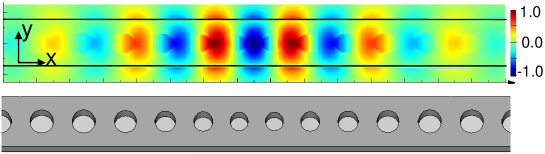
Because of the relatively low index of refraction ( = 2.0) of SiNx, the two-dimensional photonic bandgap of SiNx planar photonic crystal slabs is small, particularly when measured against a high index semiconductor like silicon. This makes the design of nanocavities in 2D photonic lattices challenging [34, 30]. To circumvent this difficulty, we consider a nanocavity for which the photonic lattice provides only one dimensional (1D) confinement, and total internal reflection provides the confinement mechanism in the other two dimensions (2D). In these “1D + 2” structures, the effective 1D bandgap, or stopband, is considerably larger than the corresponding 2D gap in a planar structure. For example, for the PhC considered in this paper, the stop-band of the “1D + 2” structure spans 13% of the center frequency, whereas the “2D + 1” hexagonal planar photonic crystal with the same pitch and hole radius yields a 2D bandgap spanning just 7% of the center frequency. The wider 1D stopband allows a greater isolation of our defect mode from the band edges and therefore higher factors in engineered defect cavities. Recently, a similar 1D design approach yielded a factor of in a high-index material () [35]. A sketch of the 1D nanocavity is shown in Figure 1, which also shows a 60 nm diamond nanocrystal positioned on top of the cavity.
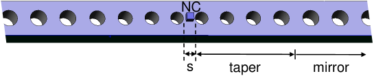
The design process consists of engineering three elements: (a) the photonic crystal mirror, (b) the taper, and (c) the cavity length. We begin by considering a free-standing SiNx ridge waveguide of thickness 200 nm and width 300 nm which supports a single TE mode. These parameters are chosen as representative of our experimental wafer, and have not been optimized in any fashion. The photonic crystal parameters, namely the hole spacing and radius , are chosen to center the resulting stop-band around the wavelength of interest ( 637 nm). Setting nm and gives a stopband over the wavelength band 593-679 nm, with a mid-gap wavelength of 636 nm, as required. We can characterize the reflectivity of the mirror using the 3D finite-difference time-domain (FDTD) method by launching a waveguide mode pulse and monitoring the reflection spectrum. The reflected light is spatially integrated over a plane perpendicular to the waveguide placed 300 nm in front of the mirror, and the loss spectrum, defined as L = 1 - R, is calculated. This spectrum quantifies the amount of light which is not reflected by the mirror and is lost due to transmission and scattering losses.
As shown by Sauvan et al. [33], the scattering losses arise in part from the mode mismatch between the waveguide and Bloch mirror modes. By tapering the mirror, the discontinuity at the interface between the cavity and mirror can be smoothed, allowing for an adiabatic transition between the modes in the two regions. The mismatch can be quantified by comparing the effective index of the Bloch mode, , to the effective index of the waveguide mode, (determined using our 3D-FDTD mode solver [36]). To gradually taper into the waveguide mode, the final segment of the mirror should support a Bloch mode such that , which determines nm. For this to work, the ratio should be maintained close to that of the uniform mirror, which implies nm. Thus, we wish to smoothly taper the photonic crystal parameters () in the mirror from () down to the values () next to the cavity. In fact, we found an improvement by tapering the radius to a smaller value than this rule would suggest, from 70 nm to 55 nm.
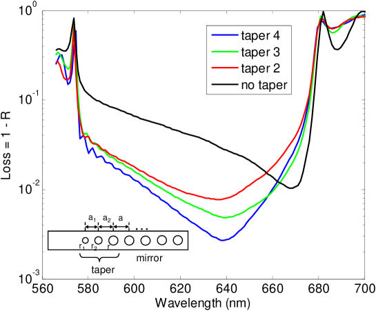
We gauge the efficacy of 2, 3, and 4 hole linear tapers according to the magnitude of , as plotted in Figure 2. The photonic crystal mirror is 17 periods in length, which was found to saturate the in-waveguide factor of the nanocavities based on these designs, as discussed below. Each increase in the taper length has the effect of further reducing the mismatch between mirror and waveguide. The 4-hole taper yields a significantly improved reflectivity and hence lower loss, giving a minimum mirror loss .
The nanocavity is defined by the gap between two taper/mirror sections, as shown in Fig. 1. In the 3D-FDTD simulation, the cavity is excited with several randomly phased and positioned dipole sources, and the factor is determined from the exponential decay of the electric field ringdown in the cavity. We also verified the factors by monitoring the power absorbed by the simulation boundaries, as discussed below, and these agree well with the ringdown values. To accurately model in a 3D-FDTD simulation the exact taper and cavity length dimensions to the scale of nanometers while maintaining tractable simulation times, we use a graded mesh approach. The mesh grid size is 5 nm in the central 0.4 0.4 0.4 m simulation volume. Outside this region, the mesh grid spacing is 10 nm for the dielectric waveguide (corresponding to 25 points per photonic lattice spacing), and is nonlinearly graded with distance in free-space away from the dielectric material. We verified the convergence of the graded mesh simulation with a 5 nm grid uniformly meshed simulation.
We consider cavities formed by the 4-segment tapered mirrors, which gave the highest reflectivity in the above analysis. The dependence of the factor on the nanocavity length is illustrated in Figure 3. The maximum obtained is 230,000 for nm. This is nearly 20 times better than the highest value reported in the literature to date [30]. In these simulations, we have not considered material absorption, which was shown by Barclay et al. [26, 37] to be a limiting factor in SiNx only for factors in the range of a few million, or scattering due to fabrication imperfections. Further optimization may be possible by optimizing the waveguide width and thickness, as well as using different (e.g. longer) taper forms.
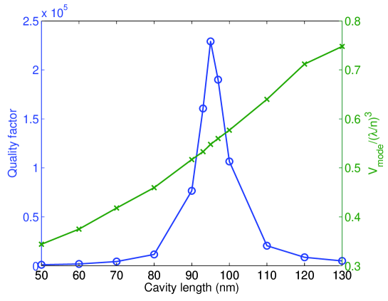
The mode volume is plotted as the green trace in Figure 3. The cavity with the maximum has a mode volume . Despite the relatively low refractive index of SiNx, this is half the effective mode volume of the recent ultra-high- photonic crystal cavities designed in high index semiconductors [28, 29, 35], demonstrating the highly attractive ultra-small size of these 1D nanocavities.
The mechanism which yields the high factor in the 4-hole tapered nanocavities is more subtle than a simple reduction of mirror loss compared to the shorter tapers. As shown in Figure 2, the loss of the 2-hole taper is improved by a factor of 3 in the 4-hole taper, but the factor of the optimal cavity based on each design is increased by a factor of almost 20. In a Fabry-Perot cavity, one would expect the factor to be proportional to the inverse loss. The difference here is that the cavity mode is derived from the propagating Bloch modes of the photonic crystal mirror, and the local structural perturbation which forms the cavity introduces a mode gap [35, 28] capable of supporting very high modes. Recently, we used a similar approach to design cavities based on semiconductor nanowires with [38]. The tapered transition from the mirror to the nanocavity not only reduces mirror loss in the simple Fabry-Perot picture, but reduces radiative loss arising from delocalization of the mode profile in -space [39]. There may also be a role played by radiation modes in recycling the mirror losses and increasing the factor, as elaborated by Lalanne et al. in Ref. [32].
For a given structure, the factor can be separated into in-waveguide, , and perpendicular, components using the relation (in analogy to the , division common in the analysis of 2D PhC microcavities [40]). is calculated by measuring the power absorbed at the boundary of the simulation within one half-wavelength of the surface of the waveguide, , and then using the definition of the Quality factor, , where is the electromagnetic energy in the resonant mode. is then determined from and the total . For a 17 period mirror, , indicating that the waveguide losses have saturated and the total losses are completely determined by out-of-waveguide loss. With a shorter photonic crystal mirror, the total drops as it is limited by in-waveguide losses. With 11 periods in the mirror, is reduced to about half the maximum value. This provides a guide for the design of an integrated in-waveguide emitter, in which light trapped or emitted into the nanocavity would couple predominantly into the waveguide mode rather than scattering off the ridge. This was the approach of Zain et al. [41], who designed a period PhC mirror in a silicon-on-insulator ridge waveguide and experimentally demonstrated a factor of 18,500 with a transmission of 85%.
3 Incorporation of a diamond nanocrystal
Now that we have optimized our photonic crystal nanocavity design, we consider exploiting this nanocavity to enhance the zero-phonon line (ZPL) emission from a NV center in a diamond nanocrystal. Coupling the emission to the nanocavity mode will lead to a Purcell enhancement of the spontaneous emission rate, and as we show below, the potential to realize quantum dynamics in the strong coupling regime.
The ideal placement of the diamond NC is in the middle of the nanocavity, where the NV center can interact with the maximal electric field of the cavity mode. It is important to quantify the effect of the NC on the cavity factor. As in the bare (unperturbed) cavity 3D-FDTD simulations, a 5 nm mesh is used in the central volume of the simulation in order to accurately model the effects of the small volume of diamond. We consider 20 nm and 40 nm sized cubic diamond NCs. Interestingly, the results reveal that the factor is not uniformly affected for all cavities. For cavities longer than 95 nm incorporating a 20 nm NC, the decreases by 10-12%, but for cavities shorter than this, the factor is actually increased. In the best cavity ( = 95 nm), the bare factor of 230,000 increases to 240,000 with the 20 nm NC. These results perhaps reflect a trade-off between the beneficial impact of the increased refractive index in the cavity center, which would be expected to raise the factor, and the deleterious effect of changing the impedance matching condition used to design the mirror tapers. As expected with the higher index cavity core, there is a reduction of about 10% in the mode volume for all cavity lengths. We conducted a similar investigation for a 40 nm cubic diamond NC located at the cavity center, and found that the vs. curve shifts to shorter cavities compared to Fig. 3, yielding a peak at nm, with a mode volume of 0.50 ()3. The main conclusion that can be drawn from this analysis is that the cavity factors are not changed by more than about 10% from the bare cavity values. The highest factor can still be achieved, and even slightly improved, and the mode volumes are slightly reduced.
Experimentally, an embedded NC might be realized by depositing a 100 nm layer of SiNx on a sacrificial layer of SiO2, placing a single diamond NC in a known position, and then depositing another 100 nm layer of SiNx to cap the structure and embed the NC in the middle. The NC position could be registered with respect to external alignment markers [42], or the position might be revealed after the SiNx regrowth by a bump on the top surface [43]. The PhC nanocavity would then be patterned around the NC, followed by removal of the SiO2. We simulated the scenario of a small 20 nm bump of SiNx on top of the cavity with an embedded 20 nm NC, and found a reduction of only about 2% in the factor of the best cavity.
An alternate approach to embedding a diamond NC would be to position the NC on top of the cavity. In [44], Koenderink et al. consider the emission enhancement of a dipole right at the semiconductor/air interface of a uniform slab 2D photonic crystal, and show that the rate can be enhanced by 5 - 10 times near the band edges. Here we model a similar scenario, except the emitter is situated on the top surface of our SiNx nanocavity. The high ratio of our nanocavity presents the possibility to yield much higher emission enhancements, as elaborated below, with a maximum Purcell factor of 1,800 for the NC on top, and 27,000 for the cavity with an embedded NC.
We consider diamond NC cubes with 3 different edge lengths: 20 nm, 40 nm, and 60 nm, and consider the effect of such a NC placed exactly above the central anti-node of the nanocavity mode. We explore the effect on the mode factor of this small dielectric perturbation (n = 2.43), and analyze the sensitivity of the to the precise positioning of the NC. The cavity design for these simulations had a maximum of 115,000 ( nm), which was not the optimal design ( nm).
The simulations are repeated for a range of NC positions to model the effect of imperfect NC placement, and the results are summarized in Figure 4. The NC position is varied over a displacement of 40 nm in the x-direction and 60 nm in the y-direction with respect to the center of the cavity, as shown by the white box in Fig. 4(a).
The results show that while the relatively large 60 nm diamond NCs have a significant impact on the mode , the situation is very promising for 40 nm and 20 nm sized NCs. The on-center factor is 47,100 for a 40 nm NC, and as the position is moved away in either the or directions from the mode center, the factor increases to a maximum of almost 74,000 at ()= (40,60) nm. Of course, for positions away from the central anti-node of the mode, the electric field strength is lower, reducing the coupling of the NC to the cavity. There will thus be a trade-off between and field strength.
For a 20 nm diamond NC, the factor is close to , or about 90% of the maximum unperturbed of the cavity, regardless of NC position. We note that Jelezko et al. [16] observed 1.5 to 2 s spin coherence times in 20 nm sized nanocrystallites of diamond. Our results show that an NC of this size has little effect on our cavity mode factor whether it is embedded in the middle or positioned on top, and therefore is a very promising candidate for cavity QED experiments.
4 Cavity QED analysis
To achieve strong coupling between a diamond NV center and a cavity, the coherent interaction rate, or vacuum Rabi frequency , must exceed the decoherence rates due to the cavity loss, , and the spontaneous emission rate, ; i.e., . The Rabi frequency is defined as , where is the single photon electric field strength. At the electric field maximum of the cavity mode,
| (1) |
where is the mode frequency, is the mode volume, and is the cavity refractive index.
The dipole moment of the NV center can be deduced from its spontaneous emission lifetime, ns [45], by using Fermi’s golden rule for an electric dipole transition [46, 47]:
| (2) |
The squared matrix element is averaged over the available emission modes. Here, is the single photon electron field at the emitter, and is the density of states in a homogeneous medium with refractive index :
| (3) |
In our context, is the refractive index of the diamond nanocrystal.
Solving for with the help of eq. (1) for (with ) gives
| (4) |
The extra factor of 3 arises from the 1/3 averaging of the squared dipolar matrix element over the random polarization of free-space modes. Note that this dipole moment is integrated over the entire spectrum of the NV emission, a point we shall return to below.
The Rabi frequency can now be evaluated from equations 4 and 1 to give
| (5) |
The label indicates that this is the maximum coherent interaction rate, which holds if the NV center is positioned at the mode maximum and aligned with its dipole moment parallel to the field vector.
When the emitter is not located at the mode maximum - e.g. if it is positioned on top of the cavity, as sketched in Fig. 1 - must be scaled by , the relative strength of the electric field at the NV location () compared to at the mode maximum (). This factor can be obtained from our FDTD simulations, and for a 20 nm NC on top of the nm cavity, it is given by .
If the NV center is embedded at the center of the cavity where the mode peaks, there is still a reduced field strength inside the NC due to the larger dielectric constant of the diamond compared to the surrounding cavity material. Maxwell’s equations dictate that the normal component of the electric field at the interface between two materials (labeled 1 and 2) satisfies the boundary condition . For the small perturbation posed by a sub-wavelength sized diamond nanocrystal, this picture will be more complicated than for a single interface between two bulk dielectrics (in which case the field would be scaled down by a factor () in the higher index diamond NC). We can again determine precisely from FDTD simulations, and for a 20 nm diamond NC at the middle of the cavity, .
For each cavity (see e.g. Fig. 3, we are now in a position to calculate the relevant cavity QED figures of merit, given by the three angular frequencies:
| (6) | |||||
| (7) | |||||
| (8) |
In a diamond NV center, the zero-phonon line only contributes about 5% of the total emission, the rest being emitted into the phonon sideband [10]. Therefore, only 5% of the total emission is coupled to the cavity mode, and must be scaled by .
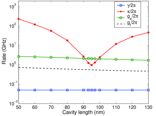
These parameters are plotted in Figure 5. The spontaneous emission rate is independent of cavity length. The Rabi frequency has a weak dependence on cavity length through and , both of which change slowly with length. The cavity field decay rate, , obviously depends strongly on cavity length, as it is proportional to . When the NC is placed on top of the cavity (black dashed line), the condition is not quite satisfied for the highest cavity. When the NC is embedded in the cavity (green line), however, the strong coupling condition is satisfied for cavities with lengths nm. At 95 nm, the single-atom cooperativity for an embedded NC is , which is a promising figure-of-merit describing the strength of the matter-field interaction. For the NC on top of the cavity, .
In the weak coupling, or “bad cavity” regime, in which the rate of cavity decoherence exceeds the coupling rate , the spontaneous emission rate will be strongly enhanced by the Purcell effect. At a temperature of 1.8 K, the emission linewidth of the ZPL corresponds to a factor of a few [48], which is much narrower than the cavity line, signifying that the full ZPL can be strongly enhanced given optimal coupling with the cavity mode. For the 95 nm cavity with an embedded diamond NC, the Purcell factor , assuming the full spectral and polarization alignment of the NV transition dipole moment with the anti-node of the cavity mode. The relative field strength at the NC position enters as a squared factor [46]. If the NC is positioned on top of the 95 nm cavity, the maximum attainable Purcell factor is about 1,800. The cavity is thus a highly promising device to enhance the photon production rate from an NV center.
5 Conclusions
In this paper, we have engineered a high- SiNx photonic crystal nanocavity with for the purpose of strongly coupling the cavity mode with a single NV center in a 20 nm diamond nanocrystal. The structure should be relatively straightforward to fabricate, as the process is based on well-known nanofabrication techniques, and it naturally integrates the cavity with an on-chip ridge waveguide, allowing a well-defined output channel to be engineered for photons confined in the cavity mode [49]. This could be achieved either by shortening the photonic mirror to decrease the in-waveguide factor, or by applying a -spoiling pulse to inject free carriers into the cavity, as has been demonstrated in recent work on dynamic perturbations in photonic nanocavities [50, 51]. We have demonstrated a cavity factor of 230,000 with an effective mode volume of 0.55 ()3, and shown that a 20 nm diamond nanocrystal located on the cavity surface reduces the by only . The same NC embedded in the middle of the cavity increases the factor while reducing the mode volume. By calculating the Rabi frequency and comparing this to the decoherence rates of the system, we have shown that the cavity with an embedded NC can operate in the strong coupling regime for realistic parameters. We anticipate these results will open new avenues for photonic crystal-based visible photonics in both classical and quantum domains.
Acknowledgements
The authors would like to thank Darrick E. Chang for his insightful comments. Murray McCutcheon would like to thank the Natural Science and Engineering Research Council of Canada for their generous support. This work is supported in part by Harvard’s National Science and Engineering Center (http://www.nsec.harvard.edu) and NSF NIRT grant ECCS- 0708905.