Tunable thermal emission at infrared frequencies via tungsten gratings
Abstract
The author investigates the manipulation of thermal emission by using one-dimensional tungsten gratings with different groove depths. It is found that, by systematically increasing the depth of the groove, the linearly polarized emission at particular frequencies can be substantially enhanced to achieve that of the blackbody radiation limit, whereas the emission in other frequency ranges shows no noticeable changes. The results can provide useful insights into the design of thermovoltaic applications.
pacs:
44.40.+a, 42.70.Qs, 42.25.Dd, 71.23.AnThermal radiation heat transfer is a ubiquitous process in nature, and thermal emission has been an active research area for many years (Planck, 1959; Siegel and Howell, 2002). The main idea behind controlling the emission spectrum of an object is to manipulate its photon density of states (DOS). The photon DOS of a natural substance such as a metal or a dielectric, can be modified slightly by changing the temperature. The recent invention of man-made structures such as photonic crystals (PCs) and plasmonic surfaces (PSs) has opened up the area of photon DOS control Joannopoulos et al. (1995); Sakoda (2001); Raether (1988); Zhang et al. (2000, 2001); Yannopapas et al. (2001); Strauf et al. (2007); Billaudeau et al. (2008). Recent years have witnessed rapid growth in the study of thermal radiation control via such artificial structures (Hesketh et al., 1986; Cornelius and Dowling, 1999; Pendry, 1999; Fleming et al., 2002; Wan and Chan, 2006; Han et al., 2007; Lee and Chan, 2007; Lee et al., 2008a, b; Wang et al., 2007; Ikeda et al., 2008). For example, radiation at infrared frequencies can be suppressed (Fleming et al., 2002) by manipulating the geometry and material parameters of metallic PCs with large band gaps over the infrared frequencies, thus allowing radiation at optical frequencies to be more efficient. However, the complexity of the fabrication process for realistic PCs remains a challenge. A structure that can be easily fabricated while providing the flexible control of thermal radiation is therefore highly desirable. Although the fabrication of bulk PC structures still presents a major challenge, textured surfaces can be made relatively easily even for sub-wavelength patterns. In addition, the advantages of bulk PCs over surfaces with man-made structures in thermal radiation control are still being debated. For instance, it is difficult to fabricate the woodpile structure used by Fleming et al. (2002) and Han et al. (2007) Although the proposed use of self-assembly techniques Velev and Kaler (2000); Jiang et al. (1999) seems promising, the tungsten inverse opal structure von Freymann et al. (2004) fabricated by such a technique has not been shown to have substantial superiority over other known PC structures in controlling thermal emission. Although extensive attention is being focused on bulk PC structures, the modification of thermal emission via textured surfaces has also been widely studied. Recently, Fleming et al. (2002), Wan and Chan (2006), and Yannopapas (2006) reported independently that a thin photonic crystal slab is sufficient to achieve the strong emission of electromagnetic radiation at desired frequencies, and that emission at other frequencies can be suppressed. Moreover, the thermal radiation effect of textured surfaces was also studied by Pendry (1999), Joulain et al. (2005), and Fu et al. (2005). In view of these recent findings, textured surfaces appear to be promising candidates for thermal radiation control. In this study, the author uses a model system consisting of tungsten gratings and investigates the effects of groove depth on emission properties. It is found that, by systematically increasing the height of the groove, the emission at particular frequencies can be tuned to achieve that of the theoretical limit, that is, the blackbody radiation limit, wheres the emission in other frequency ranges has no noticeable changes. Therefore, the tungsten gratings may be useful to the design of thermal photovoltaic devices, which require a structure that emits strongly at a particular frequency.
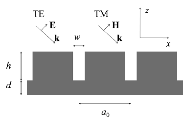
The cross-section of the model tungsten grating is shown in Fig. 1. The grating has a period of m and a thickness of m. It is considered to be optically thick because it is much thicker than the typical skin depth ( nm) of metals, thus allowing no light to penetrate it. The width of the groove is fixed at 0.3 m, and the depths are fixed at and 2.0 m. According to Kirchhoff’s law, the spectral emittance of a surface is equal to its spectral absorbance at thermal equilibrium; here, and denote the wavevector and angular frequency of the emitted radiation. The validity of Kirchhoff’s law for textured surfaces has been demonstrated by Luo et al. (2004). Therefore, to understand the emission properties of tungsten gratings, the angle-dependent absorbances are calculated using the transfer matrix method (TMM) (Bell et al., 1995). The absorbance for each k and is given by , where and are the total reflectance and transmittance of an incident wave. In our calculations, because of the large thickness of the gratings.
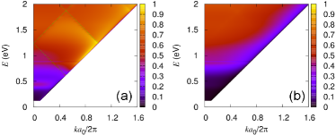
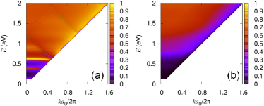
The resultant absorbance spectra for TE () and TM () polarizations are shown in Figs. 2 and 3. For the latter, no noticeable difference in absorbance between the different structures can be observed, and the overall absorbance of both structures is close to that of a plain tungsten slab. The strong absorption for eV ( m) is due to the intrinsic optical property of tungsten Rephaeli and Fan (2008). Therefore, the grating geometry does not significantly enhance absorbance for TM polarization. In contrast, the absorbance for TE polarization changes considerably with groove depth. In addition to the strong tungsten absorption at eV, strong absorption peaks are also observed for TE polarization at eV. The locations of the absorption peaks appear consistently and systematically for both m and m. In addition, the peaks exhibit typical band-folding behavior, thus indicating that they are due to the excitation of the propagating surface plasmon polaritons (SPPs) by the incident waves. To trace the origin of the absorption, the dispersion relation of the propagating SPPs is plotted on top of the absorbance spectra (Raether, 1988):
| (1) |
where is an integer, is the angular frequency, k is the in-plane wave vector in the -direction, which is related to the incident angle () by , is the speed of light, and and are, respectively, the dielectric functions of air and tungsten (Palik, 1985). As can be seen, equation (1) fits very well with the TE-absorption peaks for each grating, which indicates that the physical origin of the absorption peaks for eV is the excitation of the propagating SPPs.
We next focus on the region of eV, in which absorption should be weak for tungsten. For m, non-dispersive absorption peaks are observed at 0.45 eV ( 2.8 m). As revealed later, the enhancement of absorption is by almost a factor of 10 compared to that of a tungsten slab. In addition, when the depth increases from 0.5 m to 2.0 m, multiple peaks are observed at eV ( m) and eV ( m). Although not shown in this work, a similar scenario occurs if the groove width increases, whereas no considerable absorption peaks are observed for a groove width of less than 0.2 m. Moreover, it should be noted that at eV, the absorbance is very close to 1 and remains strong even when the incident angle is close to 90∘. These absorption peaks could be attributed to waveguide modes, as proposed by Porto et al. (1999), in which a standing wave is formed inside the groove and results in energy accumulation.
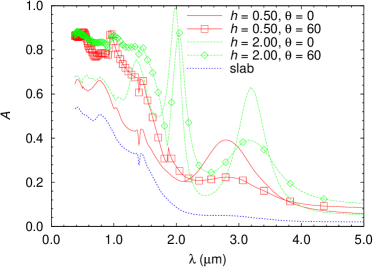
To examine the dependence of TE absorbance on groove depth, the absorbance spectra for each depth at two incident angles are plotted (0∘ and 60∘) in Fig. 4. The absorbance of a thick tungsten slab is also drawn for comparison. As can be seen, the absorbance of a flat tungsten slab is low () for near infrared (IR) wavelengths ( m), which is due to the large dielectric mismatch between tungsten and air. As the magnitude of the real part of the dielectric function drops significantly for m, the dielectric mismatch is reduced, thus resulting in the observed increase of absorbance for shorter wavelengths, and reaches a plateau value of for m. Therefore, the TM absorbances shown in Figs. 2 and 3 could mainly be attributed to the intrinsic absorption of tungsten.
In the case of the TE mode, the effects of the groove can be clearly seen. Depending on different geometries and incident angles, absorbance can be enhanced by as much as a factor of 2 with respect to that of a tungsten slab. For near IR wavelengths, the groove results in the great enhancement of absorbance at certain frequencies. For example, at normal incident (), is enhanced by almost an order of 10 at m for m, which corresponds to the peak at 0.45 eV in Fig. 2. In addition, a longer groove can result in more pronounced and sharper peaks; this is evident from the absorbance of m. In such a case, has strong and non-dispersive peaks at and 2.0 m, respectively. The peaks at m are very close to 1 and are highly non-dispersive. The absorbance peak drops 10% only when the incident angle changes from 0∘ to 60∘, and the peak position remains close to m.
We now compare the TE thermal emission spectra of different gratings, and the results are shown in Fig. 4. The thermal emission spectra are calculated by assuming Kirchhoff’s law Siegel and Howell (2002), and the thermal emission spectrum of wavevector at temperature is given by
| (2) |
where is the Planck spectrum of blackbody radiation.
As our primary aim is to investigate the effect of the groove on the radiation spectra, we ignore the temperature effect on the tungsten dielectric constant Arnold (1984); Dubrovinsky and Saxena (1997).
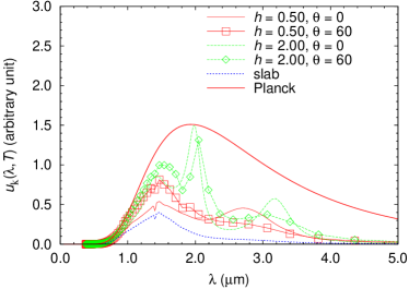
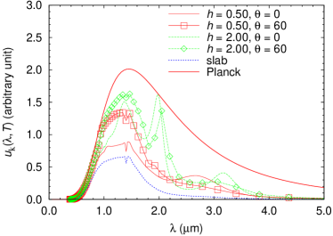
In Fig. 5, the thermal emission spectra of the surfaces corresponding to those in Fig. 4 at 1500 K are drawn and compared with that of a blackbody (). In all cases, the emission of the grating in all frequency ranges is enhanced with respect to that of a slab, with the corresponding optical spectra being close to that of a blackbody. Also, the peaks of the grating’s emission spectra are effectively red-shifted due to the strong absorption at infrared frequencies ( m), which is a direct consequence of the high level of absorbance (Figs. 2-3). Similar emission characteristics are observed when the temperature is raised to 2000 K (Fig. 6). The emission is now dominated by photons with shorter wavelengths (1.0 m), with the exception of m for m. In other words, the thermal emission of photons at m is highly robust in all angles and a wide range of temperatures ( K).
The results shown in Figs. 2-4 suggest that gratings are effective in manipulating the thermal emission of photons. By controlling groove depth, the emission peak can be tuned to the desired frequency. The reason for such emission enhancement could be attributed to the excitation of the waveguide mode, in which thermally excited photons at the resonant frequencies accumulate in the vicinity of the groove. As the excited field is strong in the air, but weak on the metallic surface, energy loss is minimal, and photons can be emitted. To show the presence of the waveguide modes, we consider, for Fabry-Pérot-like resonance, the wavelengths of the th and th resonances are related by
| (3) |
According to Figs. 5 and 6, m and 2.0 m at resonance, which gives and . As the waveguide mode is highly frequency-selective, those thermally excited photons that are not at the resonant frequencies are re-absorbed by the groove and cannot be emitted.
It should be noted that the emission peak can be tuned according to the operating temperature. For instance, the emission peak of blackbody radiation is given by Wien’s displacement law, , where mK is the Wien’s displacement constant. For K, m, which is close to the absorption peak of the m grating shown in Fig. 3. Therefore, absorption spectra (Figs. 2-4) provide useful information on how to achieve maximum emission at the desired temperature.
In this study, the thermal property of emission is modified by enhancing the emitting power of photons at frequencies at which the emitting power would be low for a plain slab. Another way to manipulate thermal emission is to suppress the emission of photons by introducing photonic or plasmonic band gaps to the system. The ultimate goal for thermal emission control is to acheive both of these on the same geometry, that is, to enhance emission in the desired frequency range while suppressing the emission of un-wanted photons. Also, in practice, the intrinsic thermal properties should be taken into account. For example, tungsten is used in this work because of its high melting temperature ( K). Depending on the operating temperature, one may choose an emitter made of other metals, and the resultant emission properties will be different from those in this work. Nevertheless, the principle of emission manipulation should remain the same.
The present study focuses on the effect of groove depth. However, the period of the grating is also an important parameter for controlling its optical properties. For example, the excitation of the SPPs shown in Figs. 2-3 is mainly controlled by periodicity, and the excitation of SPPs via various geometries has been actively studied. In partcular, it has been shown that Greffet et al. (2002); Yannopapas and Vitanov (2007) the thermal radiation emitted via SPP should be highly directional and coherent, and will resemble the state of coherence of laser radiation. The tungsten gratings are thus expected to have SPP-originated emission properties similar to those of the SiC grating of Greffet et al. (2002). However, the absorbance spectrum shown in Fig. 3a is fairly broadband even when SPPs are excited at eV (see the green dashed lines in Fig. 3a), and the emission is merely driven by the intrinsic absorption of bulk tungsten. This should be due to the small periodicity used ( m) in this work (compared to that of 6.25 m in the work of Greffet et al. (2002)). One should be able to observe SPP-driven, directional emission when the periodicity is increased, which will eventually lower the exicitation frequencies of SPP modes to frequencies below 0.6 eV. Nevertheless, the role of SPPs in the thermal emission of grating will be the subject of further study.
Finally, the calculated absorbance spectra in this work can be verified in the laboratory by measuring the zeroth order angle-dependence reflectance. As the frequencies of interest are lower than the lowest SPP excitation frequencies, the higher-order diffraction effect can be neglected. However, the measurement of emission at high temperatures remains a challenge. To conclude, our results suggest that thermal emission can be controlled flexibly via metallic arrays of different groove depths, thus resulting in an efficient infrared radiator. It is hoped that this work will provide useful insights into the design of tunable thermal emitting devices.
The author thanks Jensen Li and C. T. Chan for their discussions of this work and acknowledges the support of S. S. Lam and T. L. Wan. Computation was performed using the CUHK high-performance computing (HPC) facility. This work is supported by RGC-HK (CERG project no. 403308).
References
- Planck (1959) M. Planck, The Theory of Heat Radiation (Dover, New York, 1959).
- Siegel and Howell (2002) R. Siegel and J. R. Howell, Thermal Radiation Heat Transfer (Taylor and Francis, New York, 2002).
- Joannopoulos et al. (1995) J. D. Joannopoulos, R. D. Meade, and J. N. Winn, Photonic Crystals: Molding the Flow of Light (Princeton Universiry Press, Princeton, N. J., 1995).
- Sakoda (2001) K. Sakoda, Optical Properties of Photonic Crystals (Springer, Berlin, 2001).
- Raether (1988) H. Raether, Surface Plasmons (Springer, Berlin, 1988).
- Zhang et al. (2000) W. Y. Zhang, X. Y. Lei, Z. L. Wang, D. G. Zheng, W. Y. Tam, C. T. Chan, and P. Sheng, Phys. Rev. Lett. 84, 2853 (2000).
- Zhang et al. (2001) W. Y. Zhang, C. T. Chan, and P. Sheng, Opt. Express 8, 203 (2001).
- Yannopapas et al. (2001) V. Yannopapas, N. Stefanou, and A. Modinos, Phys. Rev. Lett. 86, 4811 (2001).
- Strauf et al. (2007) S. Strauf, N. G. Stoltz, M. T. Rakher, L. A. Coldren, P. M. Petroff, and D. Bouwmeester, Nat. Photon. 1, 704 (2007).
- Billaudeau et al. (2008) C. Billaudeau, S. Collin, F. Pardo, N. Bardou, and J.-L. Pelouard, Appl. Phys. Lett. 92, 041111 (2008).
- Hesketh et al. (1986) P. J. Hesketh, J. N. Zemel, and B. Gebhart, Nature 324, 549 (1986).
- Cornelius and Dowling (1999) C. M. Cornelius and J. P. Dowling, Phys. Rev. A 59, 4736 (1999).
- Pendry (1999) J. B. Pendry, J. Phys.: Condens. Mat. 11, 6621 (1999).
- Fleming et al. (2002) J. G. Fleming, S. Y. Lin, I. El-Kady, R. Biswas, and K. M. Ho, Nature 417, 52 (2002).
- Wan and Chan (2006) J. T. K. Wan and C. T. Chan, Appl. Phys. Lett. 89, 041915 (2006).
- Han et al. (2007) S. E. Han, A. Stein, and D. J. Norris, Phys. Rev. Lett. 99, 053906 (2007).
- Lee and Chan (2007) J. C. W. Lee and C. T. Chan, Appl. Phys. Lett. 90, 051912 (2007).
- Lee et al. (2008a) J.-H. Lee, W. Leung, T. G. Kim, K. Constant, and K.-M. Ho, Opt. Express 16, 8742 (2008a).
- Lee et al. (2008b) J.-H. Lee, J. C. W. Lee, W. Leung, M. Li, K. Constant, C. T. Chan, and K.-M. Ho, Adv. Mater. 20, 3244 (2008b).
- Wang et al. (2007) C.-M. Wang, Y.-C. Chang, M.-W. Tsai, Y.-H. Ye, C.-Y. Chen, Y.-W. Jiang, Y.-T. Chang, S.-C. Lee, and D. P. Tsai, Opt. Express 15, 14673 (2007).
- Ikeda et al. (2008) K. Ikeda, H. T. Miyazaki, T. Kasaya, K. Yamamoto, Y. Inoue, K. Fujimura, T. Kanakugi, M. Okada, K. Hatade, and S. Kitagawa, Appl. Phys. Lett. 92, 021117 (2008).
- Velev and Kaler (2000) O. D. Velev and E. W. Kaler, Adv. Mater. 12, 531 (2000).
- Jiang et al. (1999) P. Jiang, J. Bertone, K. Hwang, and V. Colvin, Chem. Mater. 11, 2132 (1999).
- von Freymann et al. (2004) G. von Freymann, S. John, M. Schulz-Dobrick, E. Vekris, N. Tétreault, S. Wong, V. Kitaev, and G. A. Ozin, Appl. Phys. Lett. 84, 224 (2004).
- Yannopapas (2006) V. Yannopapas, Phys. Rev. B 73, 113108 (2006).
- Joulain et al. (2005) K. Joulain, J.-P. Mulet, F. Marquier, R. Carminati, and J.-J. Greffet, Surf. Sci. Rep. 57, 59 (2005).
- Fu et al. (2005) C. J. Fu, Z. M. Zhang, and D. B. Tanner, Opt. Lett. 30, 1873 (2005).
- Luo et al. (2004) C. Luo, A. Narayanaswamy, G. Chen, and J. D. Joannopoulos, Phys. Rev. Lett. 93, 213905 (2004).
- Bell et al. (1995) P. M. Bell, J. B. Pendry, L. M. Moreno, and A. J. Ward, Comput. Phys. Commun. 85, 306 (1995).
- Rephaeli and Fan (2008) E. Rephaeli and S. Fan, Appl. Phys. Lett. 92, 211107 (2008).
- Palik (1985) E. D. Palik, ed., Handbook of Optical Constants of Solids (Academic Press, Orlando, 1985).
- Porto et al. (1999) J. A. Porto, F. J. García-Vidal, and J. B. Pendry, Phys. Rev. Lett. 83, 2845 (1999).
- Arnold (1984) G. S. Arnold, Appl. Opt. 23, 1434 (1984).
- Dubrovinsky and Saxena (1997) L. S. Dubrovinsky and S. K. Saxena, Phys. Chem. Miner. 24, 547 (1997).
- Greffet et al. (2002) J.-J. Greffet, R. Carminati, K. Joulain, J.-P. Mulet, S. Mainguy, and Y. Chen, Nature 416, 61 (2002).
- Yannopapas and Vitanov (2007) V. Yannopapas and N. V. Vitanov, Phys. Rev. Lett. 99, 053901 (2007).